Building a Programmable Logic Controller with a PIC16F648A Microcontroller lenguaje asembler .pdf
0 likes75 views

This document provides an overview of a book that describes how to build a programmable logic controller (PLC) using a PIC16F648A microcontroller. The book teaches advanced students and engineers how to design and use a microcontroller-based PLC. It assumes the reader has knowledge of digital logic, microcontrollers, and PLCs. The accompanying CD-ROM contains all the source code and examples from the book. The goal is to answer how one can design and implement a PLC in a way that is accessible for learning.


![xvii
Background and Use of the Book
This project was completed during the search for an answer to the follow-
ing question: How could one design and implement a programmable logic
controller (PLC)? The answer to this question was partially discovered about
15 years ago by the author in a freely available PLC project called PICBIT.
The file, called picbit.inc of PICBIT, contains the basic PLC macro definitions.
The PIC16F648A-based PLC project has been completed by the inspiration of
these macros. Of course many new features have been included within the
PIC16F648A-based PLC project to make it an almost perfect PLC. The reader
should be aware that this project does not include graphical interface PC
software as in PICBIT or in other PLCs for developing PLC programs. Rather,
PLC programs are developed by using macros as done in the Instruction
List (IL) PLC programming language. An interested and skilled reader could
well (and is encouraged to) develop graphical interface PC software for easy
use of the PIC16F648A-based PLC.
The PIC16F648A-based PLC project was first reported in a series of 22 arti-
cles published in Electronics World magazine (http:/
/www.electronicsworld.
co.uk/) between the years 2008 and 2010 [1–22]. All details of this project
can be viewed at http/
/www.meliksah.edu.tr/muzam/UZAM_PLC_with_
PIC16F648A.htm [23]. This book is based on an improved version of the
project reported in Electronics World magazine. The improvements are sum-
marized as follows:
1. The current hardware has two boards: the CPU board and the I/O
extension board. In the previous version of the hardware, the main
board consisted of the CPU board and eight inputs/eight outputs,
while in the current version, the CPU board excludes eight inputs/
eight outputs. Thus, the CPU board is smaller than the previous
main board. In addition, the current I/O extension board is also
smaller than in the previous version.
2. The hardware explained in this book consists of one CPU board and
two I/O extension boards. Therefore, the current version of the soft-
ware supports 16 inputs and 16 outputs, while the previous one sup-
ported 8 inputs and 8 outputs.
3. Clock frequency was 4 MHz in the previous version, but is 20 MHz
in the current version.
4. Someofthemacrosareimprovedcomparedwiththepreviousversions.
5. Flowcharts are provided to help the understanding of all macros
(functions).](https://image.slidesharecdn.com/buildingaprogrammablelogiccontrollerwithapic16f648amicrocontrollerlenguajeasembler-220618154203-89548f6a/85/Building-a-Programmable-Logic-Controller-with-a-PIC16F648A-Microcontroller-lenguaje-asembler-pdf-18-320.jpg)
![xviii Background and Use of the Book
In order to properly follow the topics explained in this book, it is expected
that the reader will construct his or her PIC16F648A-based PLC consist-
ing of the CPU board and two I/O extension boards using the PCB files
provided within the CD-ROM attached to this book. In this book, as the
PIC assembly is used as the programming language within the MPLAB
integrated development environment (IDE), the reader is referred to the
homepage of Microchip (http://www.microchip.com/) to obtain the latest
version of MPLAB IDE. References [24] and [25] may be useful to under-
stand some aspects of the PIC16F648A microcontroller and MPASM™
assembler, respectively.
The contents of the book’s 15 chapters are explained briefly, as follows:
1. Hardware: Inthischapter,thehardwarestructureofthePIC16F648A-
based PLC, consisting of 16 discrete inputs and 16 discrete outputs,
is explained in detail.
2. Basic software: This chapter explains the basic software structure
of the PIC16F648A-based PLC. A PLC scan cycle includes the fol-
lowing: obtain the inputs, run the user program, and update the
outputs. In addition, it is also necessary to define and initialize all
variables used within a PLC. Necessary functions are all described
as PIC assembly macros to be used in the PIC16F648A-based PLC.
The macros described in this chapter can be summarized as follows:
HC165 (for handling the inputs), HC595 (for sending the outputs),
dbncr0 and dbncr1 (for debouncing 16 inputs), initialize,
get_inputs, and send_outputs.
3. Contact and relay-based macros: The following contact and relay-
based macros are described in this chapter: ld (load), ld_not (load_
not), not, or, or_not, nor, and, and_not, nand, xor, xor_not,
xnor, out, out_not, in_out, inv_out, _set, _reset. These
macros are defined to operate on 1-bit (Boolean) variables.
4. Flip-flop macros: The following flip-flop–based macros are
described in this chapter: r_edge (rising edge), f_edge (falling
edge), latch0, latch1, dff_r (rising edge triggered D flip-flop),
dff_f (falling edge triggered D flip-flop), tff_r (rising edge trig-
gered T flip-flop), tff_f (falling edge triggered T flip-flop), jkff_r
(rising edge triggered JK flip-flop), and jkff_f (falling edge trig-
gered JK flip-flop).
5.
Timer macros: The following timer macros are described in this
chapter: TON_8 (8-bit on-delay timer), TOF_8 (8-bit off-delay timer),
TP_8 (8-bit pulse timer), and TOS_8 (8-bit oscillator timer).
6. Counter macros: The following counter macros are described in this
chapter: CTU_8 (8-bit up counter), CTD_8 (8-bit down counter), and
CTUD_8 (8-bit up/down counter).](https://image.slidesharecdn.com/buildingaprogrammablelogiccontrollerwithapic16f648amicrocontrollerlenguajeasembler-220618154203-89548f6a/85/Building-a-Programmable-Logic-Controller-with-a-PIC16F648A-Microcontroller-lenguaje-asembler-pdf-19-320.jpg)

![xx Background and Use of the Book
decod_3_8_E_AL (3×8 decoder with enable input and active low
outputs).
14. Priority encoder macros: The following priority encoder mac-
ros are described in this chapter: encod_4_2_p (4×2 priority
encoder), encod_4_2_p_E (4×2 priority encoder with enable
input), encod_8_3_p (8×3 priority encoder), encod_8_3_p_E
(8×3 priority encoder with enable input), encod_dec_bcd_p
(decimal to binary coded decimal [BCD] priority encoder), and
encod_dec_bcd_p_E (decimal to BCD priority encoder with
enable input).
15. Application example: This chapter describes an example remotely
controlled model gate system and makes use of the PIC16F648A-
based PLC to control it for different control scenarios.
Table 1 shows the general characteristics of the PIC16F648A-based PLC.
TABLE 1
General Characteristics of the PIC16F648A-Based PLC
Inputs/Outputs/Functions
Byte Addresses/
Related Bytes
Bit Addresses or Function
Numbers
16 discrete inputs
(external inputs: 5 or 24 V DC)
I0
I1
I0.0, I0.1, …, I0.7
I1.0, I1.1, …, I1.7
16 discrete outputs
(relay type outputs)
Q0
Q1
Q0.0, Q0.1, …, Q0.7
Q1.0, Q1.1, …, Q1.7
32 internal relays
(memory bits)
M0
M1
M2
M3
M0.0, M0.1, …, M0.7
M1.0, M1.1, …, M1.7
M2.0, M2.1, …, M2.7
M3.0, M3.1, …, M3.7
8 rising edge detectors RED r_edge (0, 1, …, 7)
8 falling edge detectors FED f_edge (0, 1, …, 7)
8 rising edge triggered
D flip-flop
DFF_RED
dff_r (0, 1, …, 7), regi,biti,
rego,bito
8 falling edge triggered
D flip-flop
DFF_FED
dff_f (0, 1, …, 7), regi,biti,
rego,bito
8 rising edge triggered
T flip-flop
TFF_RED
tff_r (0, 1, …, 7), regi,biti,
rego,bito
8 falling edge triggered
T flip-flop
TFF_FED
tff_f (0, 1, …, 7), regi,biti, rego,bito
8 rising edge triggered
JK flip-flop
JKFF_RED
jkff_r (0, 1, …, 7), regi,biti,
rego,bito
8 falling edge triggered
JK flip-flop
JKFF_FED
jkff_f (0, 1, …, 7), regi,biti,
rego,bito](https://image.slidesharecdn.com/buildingaprogrammablelogiccontrollerwithapic16f648amicrocontrollerlenguajeasembler-220618154203-89548f6a/85/Building-a-Programmable-Logic-Controller-with-a-PIC16F648A-Microcontroller-lenguaje-asembler-pdf-21-320.jpg)


Building a Programmable Logic Controller with a PIC16F648A Microcontroller lenguaje asembler .pdf
- 2. Building a Programmable Logic Controller with a PIC16F648A Microcontroller
- 4. CRC Press is an imprint of the Taylor & Francis Group, an informa business Boca Raton London NewYork Building a Programmable Logic Controller with a PIC16F648A Microcontroller Murat Uzam
- 5. CRC Press Taylor & Francis Group 6000 Broken Sound Parkway NW, Suite 300 Boca Raton, FL 33487-2742 © 2014 by Taylor & Francis Group, LLC CRC Press is an imprint of Taylor & Francis Group, an Informa business No claim to original U.S. Government works Version Date: 20130710 International Standard Book Number-13: 978-1-4665-8986-5 (eBook - PDF) This book contains information obtained from authentic and highly regarded sources. Reasonable efforts have been made to publish reliable data and information, but the author and publisher cannot assume responsibility for the validity of all materials or the consequences of their use. The authors and publishers have attempted to trace the copyright holders of all material reproduced in this publication and apologize to copyright holders if permission to publish in this form has not been obtained. If any copyright material has not been acknowledged please write and let us know so we may rectify in any future reprint. Except as permitted under U.S. Copyright Law, no part of this book may be reprinted, reproduced, transmitted, or utilized in any form by any electronic, mechanical, or other means, now known or hereafter invented, including photocopying, microfilming, and recording, or in any information stor- age or retrieval system, without written permission from the publishers. For permission to photocopy or use material electronically from this work, please access www.copy- right.com (http://www.copyright.com/) or contact the Copyright Clearance Center, Inc. (CCC), 222 Rosewood Drive, Danvers, MA 01923, 978-750-8400. CCC is a not-for-profit organization that pro- vides licenses and registration for a variety of users. For organizations that have been granted a pho- tocopy license by the CCC, a separate system of payment has been arranged. Trademark Notice: Product or corporate names may be trademarks or registered trademarks, and are used only for identification and explanation without intent to infringe. Visit the Taylor & Francis Web site at http://www.taylorandfrancis.com and the CRC Press Web site at http://www.crcpress.com
- 6. To my parents and family who love and support me and to my teachers and students who enriched my knowledge
- 8. vii Contents Preface.................................................................................................................... xiii Acknowledgments.................................................................................................xv Background and Use of the Book.....................................................................xvii About the Author...............................................................................................xxiii 1 Hardware of the PIC16F648A-Based PLC...................................................1 2 Basic Software................................................................................................ 11 2.1 Basic Software Structure..................................................................... 11 2.1.1 Variable Definitions................................................................12 2.1.2 Macro HC165...........................................................................21 2.1.3 Macro HC595...........................................................................21 2.2 Elimination of Contact Bouncing Problem in the PIC16F648A-Based PLC.......................................................................22 2.2.1 Contact Bouncing Problem....................................................22 2.2.2 Understanding a Generic Single I/O Contact Debouncer.....24 2.2.3 Debouncer Macros dbncr0 and dbncr1...........................25 2.3 Basic Macros of the PIC16F648A-Based PLC....................................31 2.3.1 Macro initialize...............................................................31 2.3.2 Macro get_inputs...............................................................32 2.3.3 Macro send_outputs..........................................................33 2.4 Example Program................................................................................34 3 Contact and Relay-Based Macros...............................................................37 3.1 Macro ld (load)....................................................................................38 3.2 Macro ld_not (load not)....................................................................39 3.3 Macro not.............................................................................................40 3.4 Macro or...............................................................................................41 3.5 Macro or_not......................................................................................42 3.6 Macro nor.............................................................................................42 3.7 Macro and.............................................................................................44 3.8 Macro and_not...................................................................................46 3.9 Macro nand...........................................................................................47 3.10 Macro xor.............................................................................................47 3.11 Macro xor_not...................................................................................49 3.12 Macro xnor...........................................................................................49 3.13 Macro out.............................................................................................51 3.14 Macro out_not...................................................................................53 3.15 Macro in_out......................................................................................54 3.16 Macro inv_out...................................................................................56
- 9. viii Contents 3.17 Macro _set..........................................................................................57 3.18 Macro _reset......................................................................................58 3.19 Examples for Contact and Relay-Based Macros..............................59 4 Flip-Flop Macros............................................................................................67 4.1 Macro r_edge (Rising Edge Detector).............................................68 4.2 Macro f_edge (Falling Edge Detector)............................................70 4.3 Macro latch1 (D Latch with Active High Enable)........................72 4.4 Macro latch0 (D Latch with Active Low Enable).........................72 4.5 Macro dff_r (Rising Edge Triggered D Flip-Flop)........................ 74 4.6 Macro dff_f (Falling Edge Triggered D Flip-Flop).......................77 4.7 Macro tff_r (Rising Edge Triggered T Flip-Flop)........................80 4.8 Macro tff_f (Falling Edge Triggered T Flip-Flop).......................82 4.9 Macro jkff_r (Rising Edge Triggered JK Flip-Flop)....................82 4.10 Macro jkff_f (Falling Edge Triggered JK Flip-Flop)...................86 4.11 Examples for Flip-Flop Macros..........................................................88 5 Timer Macros..................................................................................................97 5.1 On-Delay Timer (TON).......................................................................97 5.2 Macro TON_8 (8-Bit On-Delay Timer)...............................................98 5.3 Off-Delay Timer (TOF)...................................................................... 102 5.4 Macro TOF_8 (8-Bit Off-Delay Timer)............................................. 105 5.5 Pulse Timer (TP)................................................................................. 107 5.6 Macro TP_8 (8-Bit Pulse Timer)....................................................... 108 5.7 Oscillator Timer (TOS)...................................................................... 111 5.8 Macro TOS_8 (8-Bit Oscillator Timer)............................................. 112 5.9 Example for Timer Macros............................................................... 115 6 Counter Macros............................................................................................ 121 6.1 Move and Load Macros..................................................................... 121 6.2 Counter Macros..................................................................................123 6.3 Up Counter (CTU).............................................................................. 124 6.4 Macro CTU_8 (8-Bit Up Counter).....................................................126 6.5 Down Counter (CTD)........................................................................129 6.6 Macro CTD_8 (8-Bit Down Counter)...............................................130 6.7 Up/Down Counter (CTUD).............................................................. 132 6.8 Macro CTUD_8 (8-Bit Up/Down Counter)......................................133 6.9 Examples for Counter Macros..........................................................136 7 Comparison Macros.................................................................................... 143 7.1 Macro R1_GT_R2............................................................................... 144 7.2 Macro R1_GE_R2............................................................................... 144 7.3 Macro R1_EQ_R2............................................................................... 146 7.4 Macro R1_LT_R2............................................................................... 147 7.5 Macro R1_LE_R2............................................................................... 148
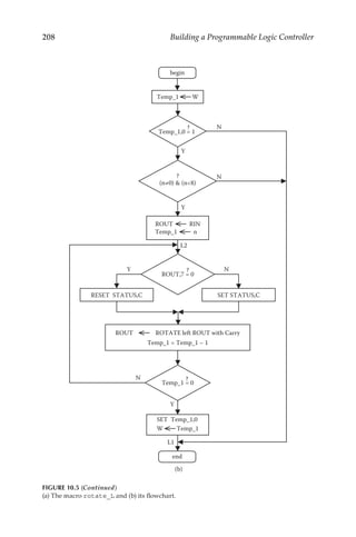
- 10. ix Contents 7.6 Macro R1_NE_R2...............................................................................150 7.7 Macro R_GT_K.................................................................................... 151 7.8 Macro R_GE_K.................................................................................... 151 7.9 Macro R_EQ_K....................................................................................153 7.10 Macro R_LT_K....................................................................................154 7.11 Macro R_LE_K....................................................................................155 7.12 Macro R_NE_K.................................................................................... 157 7.13 Examples for Comparison Macros..................................................158 8 Arithmetical Macros................................................................................... 163 8.1 Macro R1addR2.................................................................................164 8.2 Macro RaddK...................................................................................... 165 8.3 Macro R1subR2................................................................................. 165 8.4 Macro RsubK...................................................................................... 167 8.5 Macro incR......................................................................................... 168 8.6 Macro decR......................................................................................... 169 8.7 Examples for Arithmetical Macros.................................................. 170 9 Logical Macros............................................................................................. 175 9.1 Macro R1andR2................................................................................. 176 9.2 Macro RandK......................................................................................177 9.3 Macro R1nandR2...............................................................................177 9.4 Macro RnandK.................................................................................... 179 9.5 Macro R1orR2....................................................................................180 9.6 Macro RorK......................................................................................... 181 9.7 Macro R1norR2................................................................................. 182 9.8 Macro RnorK......................................................................................183 9.9 Macro R1xorR2.................................................................................185 9.10 Macro RxorK...................................................................................... 186 9.11 Macro R1xnorR2............................................................................... 187 9.12 Macro RxnorK.................................................................................... 187 9.13 Macro inv_R...................................................................................... 189 9.14 Example for Logical Macros.............................................................190 10 Shift and Rotate Macros.............................................................................199 10.1 Macro shift_R.................................................................................199 10.2 Macro shift_L.................................................................................200 10.3 Macro rotate_R...............................................................................201 10.4 Macro rotate_L...............................................................................207 10.5 Macro Swap.........................................................................................209 10.6 Examples for Shift and Rotate Macros............................................ 210 11 Multiplexer Macros.....................................................................................225 11.1 Macro mux_2_1.................................................................................225 11.2 Macro mux_2_1_E.............................................................................226
- 11. x Contents 11.3 Macro mux_4_1.................................................................................227 11.4 Macro mux_4_1_E.............................................................................228 11.5 Macro mux_8_1.................................................................................232 11.6 Macro mux_8_1_E.............................................................................233 11.7 Examples for Multiplexer Macros....................................................233 12 Demultiplexer Macros................................................................................243 12.1 Macro Dmux_1_2...............................................................................243 12.2 Macro Dmux_1_2_E..........................................................................244 12.3 Macro Dmux_1_4...............................................................................245 12.4 Macro Dmux_1_4_E..........................................................................246 12.5 Macro Dmux_1_8...............................................................................251 12.6 Macro Dmux_1_8_E..........................................................................252 12.7 Examples for Demultiplexer Macros...............................................252 13 Decoder Macros...........................................................................................263 13.1 Macro decod_1_2.............................................................................264 13.2 Macro decod_1_2_AL.....................................................................265 13.3 Macro decod_1_2_E........................................................................266 13.4 Macro decod_1_2_E_AL.................................................................268 13.5 Macro decod_2_4.............................................................................269 13.6 Macro decod_2_4_AL.....................................................................270 13.7 Macro decod_2_4_E........................................................................273 13.8 Macro decod_2_4_E_AL.................................................................273 13.9 Macro decod_3_8............................................................................. 276 13.10 Macro decod_3_8_AL.....................................................................280 13.11 Macro decod_3_8_E........................................................................280 13.12 Macro decod_3_8_E_AL.................................................................283 13.13 Examples for Decoder Macros.........................................................286 14 Priority Encoder Macros.............................................................................295 14.1 Macro encod_4_2_p........................................................................296 14.2 Macro encod_4_2_p_E...................................................................298 14.3 Macro encod_8_3_p........................................................................300 14.4 Macro encod_8_3_p_E...................................................................303 14.5 Macro encod_dec_bcd_p..............................................................303 14.6 Macro encod_dec_bcd_p_E.........................................................304 14.7 Examples for Priority Encoder Macros........................................... 312 15 Application Example................................................................................... 319 15.1 Remotely Controlled Model Gate System....................................... 319 15.2 Control Scenarios for the Model Gate System............................... 321 15.3 Solutions for the Control Scenarios.................................................323 15.3.1 Solution for the First Scenario............................................. 324 15.3.2 Solution for the Second Scenario........................................ 324
- 12. xi Contents 15.3.3 Solution for the Third Scenario...........................................325 15.3.4 Solution for the Fourth Scenario.........................................326 15.3.5 Solution for the Fifth Scenario............................................327 15.3.6 Solution for the Sixth Scenario............................................328 15.3.7 Solution for the Seventh Scenario.......................................329 15.3.8 Solution for the Eighth Scenario.........................................330 About the CD-ROM...........................................................................................337 References............................................................................................................339 Index......................................................................................................................341
- 14. xiii Preface Programmable logic controllers (PLCs) have been used extensively in indus- try for the past five decades. PLC manufacturers offer different PLCs in terms of functions, program memories, and the number of inputs/outputs (I/Os), ranging from a few to thousands of I/Os. The design and implementation of PLCs have long been a secret of the PLC manufacturers. Recently, a serious work was reported by the author of this book to describe a microcontroller- based implementation of a PLC. With a series of 22 articles published in Electronics World magazine (http/ /www.electronicsworld.co.uk/) between the years 2008 and 2010, the design and implementation of a PIC16F648A- based PLC were described. This book is based on an improved version of the project reported in Electronics World magazine. This book is written for advanced students, practicing engineers, and hob- byists who want to learn how to design and use a microcontroller-based PLC. The book assumes the reader has taken courses in digital logic design, microcontrollers, and PLCs. In addition, the reader is expected to be familiar with the PIC16F series of microcontrollers and to have been exposed to writ- ing programs using PIC assembly language within an MPLAB integrated development environment. The CD-ROM that accompanies this book contains all the program source files and hex files for the examples described in the book. In addition, PCB files of the CPU and I/O extension boards of the PIC16F648A-based PLC are also included on the CD-ROM. Dr. Murat Uzam Melikşah Üniversitesi Mühendislik-Mimarlık Fakültesi Elektrik-Elektronik Mühendisliği Bölümü Talas, Kayseri Turkey
- 16. xv Acknowledgments I am grateful to Dr. Gökhan Gelen (gokhan_gelen@hotmail.com) for his great effort in drawing the printed circuit boards (PCBs) and for producing the pro- totypes of the CPU board and the I/O extension board. Without his help this project may have been delayed for years.
- 18. xvii Background and Use of the Book This project was completed during the search for an answer to the follow- ing question: How could one design and implement a programmable logic controller (PLC)? The answer to this question was partially discovered about 15 years ago by the author in a freely available PLC project called PICBIT. The file, called picbit.inc of PICBIT, contains the basic PLC macro definitions. The PIC16F648A-based PLC project has been completed by the inspiration of these macros. Of course many new features have been included within the PIC16F648A-based PLC project to make it an almost perfect PLC. The reader should be aware that this project does not include graphical interface PC software as in PICBIT or in other PLCs for developing PLC programs. Rather, PLC programs are developed by using macros as done in the Instruction List (IL) PLC programming language. An interested and skilled reader could well (and is encouraged to) develop graphical interface PC software for easy use of the PIC16F648A-based PLC. The PIC16F648A-based PLC project was first reported in a series of 22 arti- cles published in Electronics World magazine (http:/ /www.electronicsworld. co.uk/) between the years 2008 and 2010 [1–22]. All details of this project can be viewed at http/ /www.meliksah.edu.tr/muzam/UZAM_PLC_with_ PIC16F648A.htm [23]. This book is based on an improved version of the project reported in Electronics World magazine. The improvements are sum- marized as follows: 1. The current hardware has two boards: the CPU board and the I/O extension board. In the previous version of the hardware, the main board consisted of the CPU board and eight inputs/eight outputs, while in the current version, the CPU board excludes eight inputs/ eight outputs. Thus, the CPU board is smaller than the previous main board. In addition, the current I/O extension board is also smaller than in the previous version. 2. The hardware explained in this book consists of one CPU board and two I/O extension boards. Therefore, the current version of the soft- ware supports 16 inputs and 16 outputs, while the previous one sup- ported 8 inputs and 8 outputs. 3. Clock frequency was 4 MHz in the previous version, but is 20 MHz in the current version. 4. Someofthemacrosareimprovedcomparedwiththepreviousversions. 5. Flowcharts are provided to help the understanding of all macros (functions).
- 19. xviii Background and Use of the Book In order to properly follow the topics explained in this book, it is expected that the reader will construct his or her PIC16F648A-based PLC consist- ing of the CPU board and two I/O extension boards using the PCB files provided within the CD-ROM attached to this book. In this book, as the PIC assembly is used as the programming language within the MPLAB integrated development environment (IDE), the reader is referred to the homepage of Microchip (http://www.microchip.com/) to obtain the latest version of MPLAB IDE. References [24] and [25] may be useful to under- stand some aspects of the PIC16F648A microcontroller and MPASM™ assembler, respectively. The contents of the book’s 15 chapters are explained briefly, as follows: 1. Hardware: Inthischapter,thehardwarestructureofthePIC16F648A- based PLC, consisting of 16 discrete inputs and 16 discrete outputs, is explained in detail. 2. Basic software: This chapter explains the basic software structure of the PIC16F648A-based PLC. A PLC scan cycle includes the fol- lowing: obtain the inputs, run the user program, and update the outputs. In addition, it is also necessary to define and initialize all variables used within a PLC. Necessary functions are all described as PIC assembly macros to be used in the PIC16F648A-based PLC. The macros described in this chapter can be summarized as follows: HC165 (for handling the inputs), HC595 (for sending the outputs), dbncr0 and dbncr1 (for debouncing 16 inputs), initialize, get_inputs, and send_outputs. 3. Contact and relay-based macros: The following contact and relay- based macros are described in this chapter: ld (load), ld_not (load_ not), not, or, or_not, nor, and, and_not, nand, xor, xor_not, xnor, out, out_not, in_out, inv_out, _set, _reset. These macros are defined to operate on 1-bit (Boolean) variables. 4. Flip-flop macros: The following flip-flop–based macros are described in this chapter: r_edge (rising edge), f_edge (falling edge), latch0, latch1, dff_r (rising edge triggered D flip-flop), dff_f (falling edge triggered D flip-flop), tff_r (rising edge trig- gered T flip-flop), tff_f (falling edge triggered T flip-flop), jkff_r (rising edge triggered JK flip-flop), and jkff_f (falling edge trig- gered JK flip-flop). 5. Timer macros: The following timer macros are described in this chapter: TON_8 (8-bit on-delay timer), TOF_8 (8-bit off-delay timer), TP_8 (8-bit pulse timer), and TOS_8 (8-bit oscillator timer). 6. Counter macros: The following counter macros are described in this chapter: CTU_8 (8-bit up counter), CTD_8 (8-bit down counter), and CTUD_8 (8-bit up/down counter).
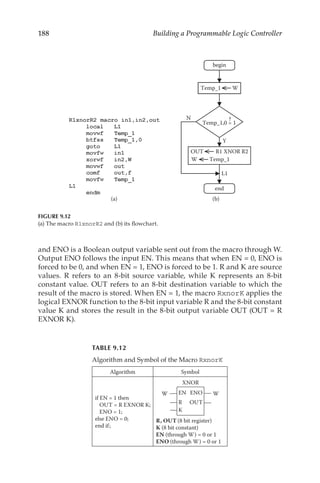
- 20. xix Background and Use of the Book 7. Comparison macros: The comparison macros are described in this chapter. The contents of two registers (R1 and R2) are compared according to the following: GT (greater than, >), GE (greater than or equal to, ≥), EQ (equal to, =), LT (less than, <), LE (less than or equal to, ≤), and NE (not equal to, ≠). Similar comparison macros are also described for comparing the contents of an 8-bit register (R) with an 8-bit constant (K). 8. Arithmetical macros: The arithmetical macros are described in this chapter. The following operators are applied to the contents of two registers (R1 and R2): ADD, SUB (subtract), INC (increment), and DEC (decrement). Similar arithmetical macros are also described, to be used with the contents of an 8-bit register (R) and an 8-bit con- stant (K). 9. Logical macros: The following logical macros are described in this chapter: inv_R, AND, NAND, OR, NOR, XOR, and XNOR. These macros are applied to an 8-bit register (R1) with another register (R2) or an 8-bit constant (K). 10. Shift and rotate macros: The following shift and rotate macros are described in this chapter: SHIFT_R (shift right the content of reg- ister R), SHIFT_L (shift left the content of register R), ROTATE_R (rotate right the content of register R), ROTATE_L (rotate left the content of register R), and SWAP (swap the nibbles of a register). 11. Multiplexer macros: The following multiplexer macros are described in this chapter: mux_2_1 (2×1 MUX), mux_2_1_E (2×1 MUX with enable input), mux_4_1 (4×1 MUX), mux_4_1_E (4×1 MUX with enable input), mux_8_1 (8×1 MUX), and mux_8_1_E (8×1 MUX with enable input). 12. Demultiplexer macros: The following demultiplexer macros are described in this chapter: Dmux_1_2 (1×2 DMUX), Dmux_1_2_E (1×2 DMUX with enable input), Dmux_1_4 (1×4 DMUX), Dmux_1_4_E (1×4 DMUX with enable input), Dmux_1_8 (1×8 DMUX), and Dmux_1_8_E (1×8 DMUX with enable input). 13. Decoder macros: The following decoder macros are described in this chapter: decod_1_2 (1×2 decoder), decod_1_2_AL (1×2 decoder with active low outputs), decod_1_2_E (1×2 decoder with enable input), decod_1_2_E_AL (1×2 decoder with enable input and active low outputs), decod_2_4 (2×4 decoder), decod_2_4_ AL (2×4 decoder with active low outputs), decod_2_4_E (2×4 decoder with enable input), decod_2_4_E_AL (2×4 decoder with enable input and active low outputs), decod_3_8 (3×8 decoder), decod_3_8_AL (3×8 decoder with active low out- puts), decod_3_8_E (3×8 decoder with enable input), and
- 21. xx Background and Use of the Book decod_3_8_E_AL (3×8 decoder with enable input and active low outputs). 14. Priority encoder macros: The following priority encoder mac- ros are described in this chapter: encod_4_2_p (4×2 priority encoder), encod_4_2_p_E (4×2 priority encoder with enable input), encod_8_3_p (8×3 priority encoder), encod_8_3_p_E (8×3 priority encoder with enable input), encod_dec_bcd_p (decimal to binary coded decimal [BCD] priority encoder), and encod_dec_bcd_p_E (decimal to BCD priority encoder with enable input). 15. Application example: This chapter describes an example remotely controlled model gate system and makes use of the PIC16F648A- based PLC to control it for different control scenarios. Table 1 shows the general characteristics of the PIC16F648A-based PLC. TABLE 1 General Characteristics of the PIC16F648A-Based PLC Inputs/Outputs/Functions Byte Addresses/ Related Bytes Bit Addresses or Function Numbers 16 discrete inputs (external inputs: 5 or 24 V DC) I0 I1 I0.0, I0.1, …, I0.7 I1.0, I1.1, …, I1.7 16 discrete outputs (relay type outputs) Q0 Q1 Q0.0, Q0.1, …, Q0.7 Q1.0, Q1.1, …, Q1.7 32 internal relays (memory bits) M0 M1 M2 M3 M0.0, M0.1, …, M0.7 M1.0, M1.1, …, M1.7 M2.0, M2.1, …, M2.7 M3.0, M3.1, …, M3.7 8 rising edge detectors RED r_edge (0, 1, …, 7) 8 falling edge detectors FED f_edge (0, 1, …, 7) 8 rising edge triggered D flip-flop DFF_RED dff_r (0, 1, …, 7), regi,biti, rego,bito 8 falling edge triggered D flip-flop DFF_FED dff_f (0, 1, …, 7), regi,biti, rego,bito 8 rising edge triggered T flip-flop TFF_RED tff_r (0, 1, …, 7), regi,biti, rego,bito 8 falling edge triggered T flip-flop TFF_FED tff_f (0, 1, …, 7), regi,biti, rego,bito 8 rising edge triggered JK flip-flop JKFF_RED jkff_r (0, 1, …, 7), regi,biti, rego,bito 8 falling edge triggered JK flip-flop JKFF_FED jkff_f (0, 1, …, 7), regi,biti, rego,bito
- 22. xxi Background and Use of the Book TABLE 1 (CONTINUED) General Characteristics of the PIC16F648A-Based PLC Inputs/Outputs/Functions Byte Addresses/ Related Bytes Bit Addresses or Function Numbers 8 on-delay timers TON8, TON8+1, …, TON8+7 TON8_Q TON8_RED TON8_Q0 TON8_Q1, … TON8_Q7 8 off-delay timers TOF8, TOF8+1, …, TOF8+7, TOF8_Q TOF8_RED TOF8_Q0 TOF8_Q1, … TOF8_Q7 8 pulse timers TP8, TP8+1, …, TP8+7, TP8_Q TP8_RED1 TP8_RED2 TP8_Q0 TP8_Q1, … TP8_Q7 8 oscillator timers TOS8, TOS8+1, …, TOS8+7 TOS8_Q TOS8_RED TOS8_Q0 TOS8_Q1, … TOS8_Q7 8 counters CV8, CV8+1, …, CV8+7 CTU8_Q0 CTU8_Q1, … CTU8_Q7 CTU: up counter CTU8_Q CTU8_RED CTD8_Q CTD8_RED or CTD8_Q0 CTD8_Q1, … CTD8_Q7 CTD: down counter CTUD8_Q CTUD8_RED or CTUD8_Q0 CTUD8_Q1, … CTUD8_Q7 CTUD: up/down counter Note: regi,biti, input bit; rego,bito, output bit. At any time, a total of eight different counters can be used.
- 24. xxiii About the Author Murat Uzam was borned in Söke, Turkey, in 1968. He received his BSc and MSc degrees from the Electrical Engineering Department of Yıldız Technical University, İstanbul, Turkey, in 1989 and 1991, respectively. He received his PhD degree from the University of Salford, Salford, UK, in 1998. He is currently a professor in the Department of Electrical and Electronics Engineering at Melikşah University in Kayseri, Turkey. Dr. Uzam’s research interests include the design and implementa- tion of discrete event control systems modeled by Petri nets (PN) and, in particular, deadlock prevention/ liveness enforcement in flexible man- ufacturing systems, Programmable Logic Controllers (PLCs), microcontrollers (especially PIC microcontrollers), and the design of microcontroller-based PLCs. The details of his studies are accessible from his web page: http:/ /www.meliksah.edu.tr/muzam.
- 26. 1 1 Hardware of the PIC16F648A-Based PLC The hardware of the PIC16F648A-based programmable logic controller (PLC) consists of two parts: the CPU board and the I/O extension board. The schematic diagram and the photograph of the PIC16F648A-based PLC CPU board are shown in Figures 1.1 and 1.2, respectively. The CPU board contains mainly three sections: power, programming, and CPU (central processor unit). The power section accepts 12 V AC input and produces two DC outputs: 12 V DC, to be used as the operating voltage of relays, and 5 V DC, to be used for ICs, inputs, etc. The programming section deals with the programming of the PIC16F648A microcontroller. For programming the PIC16F648A in circuit, it is necessary to use PIC programmer hardware and software with In Circuit Serial Programming (ICSP) capability. For related hardware and software to be used for programming the PIC16F648A-based PLC, please visit the follow- ing web page: http:/ /www.meliksah.edu.tr/muzam/. For other types of USB, serial, or parallel port PIC programmers the reader is expected to make nec- essary arrangements. The ICSP connector takes the lines VPP(MCLR), VDD, VSS(GND), DATA (RB7), and CLOCK (RB6) from the PIC programmer hard- ware through a properly prepared cable, and it connects them to a four-pole double-throw (4PDT) switch. There are two positions of the 4PDT switch. As seen from Figure 1.1, in one position of the 4PDT switch, PIC16F648A is ready to be programmed, and in the other position the loaded program is run. For properly programming the PIC16F648A by means of a PIC program- mer and the 4PDT switch, it is also a necessity to switch off the power switch. The CPU section consists of the PIC16F648A microcontroller. In the project reported in this book, the PLC is fixed to run at 20 MHz with an external oscillator. This frequency is fixed because time delays are calculated based on this speed. By means of two switches, SW1 and SW2, it is also possible to use another internal or external oscillator with different crystal frequen- cies. When doing so, time delay functions must be calculated accordingly. SW3 connects the RA5 pin either to one pole of the 4PDT switch or to the future extension connector. When programming PIC16F648A, RA5 should be connected to the 4PDT switch. RB0, RB6, and RB7 pins are all reserved to be used for 8-bit parallel-to-serial converter register 74HC/LS165. Through these three pins and with added 74HC/LS165 registers, we can describe as many inputs as necessary. RB0, RB6, and RB7 are the data in, clock in, and shift/load pins, respectively. Similarly, RB3, RB4, and RB5 pins are all reserved to be used for 8-bit serial-to-parallel converter register/driver TPIC6B595. Through these three pins and with added TPIC6B595 registers,
- 27. 2 Building a Programmable Logic Controller 12V AC In Reset ICSP Connector 4PDT Switch Future Extension Connector The PIC16F648A-Based PLC CPU Board PIC16F648A I/O Extension connector FIGURE 1.1 Schematic diagram of the CPU board.
- 28. 3 Hardware of the PIC16F648A-Based PLC FIGURE 1.2 Photograph of the CPU board.
- 29. 4 Building a Programmable Logic Controller we can describe as many outputs as necessary. RB3, RB4, and RB5 are the clock out, data out, and latch out pins, respectively. The remaining unused pins of the PIC16F648A are connected to the future extension con- nector. PIC16F648A provides the following: flash program memory (words), 4096; RAM data memory (bytes), 256; and EEPROM data memory (bytes), 256. The PIC16F648A-based PLC macros make use of registers defined in RAM data memory. Note that it may be possible to use PIC16F628A as the CPU, but one has to bear in mind that PIC16F628A provides the following: flash program memory (words), 2048; RAM data memory (bytes), 224; and EEPROM data memory (bytes), 128. In that case, it is necessary to take care of the usage of RAM data memory. Figures 1.3 and 1.4 show the schematic diagram and photograph of the I/O extension board, respectively. The I/O extension board contains mainly two sections: eight discrete inputs and eight discrete outputs. The I/O extension connector DB9M seen on the left connects the I/O extension board to the CPU board or to a previous I/O extension board. Similarly, the I/O extension Q.0 Q.1 Q.2 Q.3 Q.4 Q.5 Q.6 Q.7 I.0 I.1 I.2 I.3 I.4 I.5 I.6 I.7 The PIC16F648A Based PLC I/O Extension Board From the CPU Board or From a previous I/O Extension Board TPIC6B595 To the next I/O Extension Board FIGURE 1.3 Schematic diagram of the I/O extension board.
- 30. 5 Hardware of the PIC16F648A-Based PLC connector DB9F seen on the right connects the I/O extension board to a next I/O extension board. In this way we can connect as many I/O extension boards as necessary. Five-volt DC and 12 V DC are taken from the CPU board or from a previous I/O extension board, and they are passed to the next I/O extension boards. All I/O data are sent to and taken from all the connected extension I/O boards by means of I/O extension connectors DB9M and DB9F. The inputs section introduces eight discrete inputs for the PIC16F648A-based PLC (called I0.0, I0.1, …, I0.7 for the first I/O extension board). Five-volt DC or 24 V DC input signals can be accepted by each input. These external input signals are isolated from the other parts of the hardware by using NPN type opto-couplers (e.g., 4N25). For simulating input signals, one can use onboard push buttons as temporary inputs and slide switches as permanent inputs. In the beginning of each PLC scan cycle (get_inputs) the 74HC/LS165 is loaded (RB7 (shift/load) = 0) with the level of eight inputs and then these FIGURE 1.4 Photograph of the I/O extension board.
- 31. 6 Building a Programmable Logic Controller The PIC16F648A-Based PLC I/O Extension Board 0 The PIC16F648A-Based PLC CPU Board The PIC16F648A-Based PLC I/O Extension Board 1 )URPWKH 38%RDUG RU IURP DSUHYLRXV ,2([WHQVLRQ%RDUG )URPWKH 38%RDUG RU IURP DSUHYLRXV ,2([WHQVLRQ%RDUG FIGURE 1.5 Schematic diagram of the CPU board plus two I/O extension boards.
- 32. 7 Hardware of the PIC16F648A-Based PLC FIGURE 1.6 Photograph of the CPU board plus two I/O extension boards.
- 33. 8 Building a Programmable Logic Controller FIGURE 1.7 Photograph of the CPU board plus two I/O extension boards and a USB PIC programmer.
- 34. 9 Hardware of the PIC16F648A-Based PLC data are serially clocked in (when RB7 = 1; through RB0 data in and RB6 clock in pins). If there is only one I/O extension board used, then eight clock_in signals are enough to get the eight input signals. For each addi- tional I/O extension board, eight more clock_in signals are necessary. The serial data coming from the I/O extension board(s) are taken from the SI input of the 74HC/LS165. TheoutputssectionintroduceseightdiscreterelayoutputsforthePIC16F648A- based PLC (called Q0.0, Q0.1, …, Q0.7 for the first I/O extension board). Each relay operates with 12 V DC and is driven by an 8-bit serial-to-parallel converter register/driver TPIC6B595. Relays have single-pole double-throw (SPDT) con- tacts with C (common), NC (normally closed), and NO (normally open) termi- nals. At the end of each PLC scan cycle (send_outputs) the output data are serially clocked out (through RB3 clock out and RB4 data out pins) and finally latched within the TPIC6B595. If there is only one I/O extension board used, then eight clock_out signals are enough to send the eight output sig- nals. For each additional I/O extension board, eight more clock_out signals are necessary. The serial data going to the I/O extension board(s) are sent out from the SER OUT (pin 18) of the TPIC6B595. The PCB design files of both the CPU board and the I/O extension board can be obtained from the CD-ROM attached to this book. Note that in the PCB design of the CPU board and the I/O extension board, some lines of I/O extension connectors DB9M and DB9F are different from the ones shown in Figures 1.1 and 1.3. The project reported in this book makes use of a CPU board and two I/O extension boards, as can be seen from the schematic diagram and pho- tograph depicted in Figures 1.5 and 1.6, respectively. Thus, in total there are 16 inputs and 16 outputs. Figure 1.7 shows the PIC16F648A-based PLC consisting of a CPU board, I/O extension boards, 12 V DC adapter, and USB PIC programmer.
- 36. 11 2 Basic Software In this chapter, the basic software of the PIC16F648A-based PLC is explained. A PLC scan cycle includes the following: obtain the inputs, run the user pro- gram, and update the outputs. It is also necessary to define and initialize all variables used within a PLC. Necessary functions are all described as PIC assembly macros to be used in the PIC16F648A-based PLC. The macros described in this chapter could be summarized as follows: HC165 (for han- dling the inputs), HC595 (for sending the outputs), dbncr0 and dbncr1 (for debouncing the inputs), initialize, get_inputs, and send_outputs. In addition, the concept of contact bouncing and how it is solved in the PIC16F648A-based PLC is explained in detail. 2.1 Basic Software Structure The basic software of the PIC16F648A-based PLC makes use of general pur- pose 8-bit registers of static random-access memory (SRAM) data memory of the PIC16F648A microcontroller. For the sake of simplicity, we restrict our- selves to use only BANK 0; i.e., all macros, including the basic definitions explained here, are defined by means of 8-bit SRAM registers of BANK 0. The file definitions.inc, included within the CD-ROM attached to this book, contains all basic macros and definitions necessary for the PIC16F648A-based PLC. In this chapter, we will explain the contents of this file. First, let us look at the file called UZAM_plc_16i16o_ex1.asm, the view of which is shown in Figure 2.1. As is well known, a PLC scan cycle includes the following: obtain the inputs, run the user program, and update the outputs. This cycle is repeated as long as the PLC runs. Before getting into these endless PLC scan cycles, the initial conditions of the PLC are set up in the initialization stage. These main steps can be seen from Figure 2.1, where initialize is a macro for setting up the initial conditions, get_inputs is a macro for get- ting and handling the inputs, and send_outputs is a macro for updating the outputs. The user PLC program must be placed between get_inputs and send_outputs. The endless PLC scan cycles are obtained by means of the label “scan” and the instruction “goto scan.” The PIC16F648A-based PLC is fixed to run at 20 MHz with an external oscillator. The watchdog timer is used to prevent user program lockups. As
- 37. 12 Building a Programmable Logic Controller will be explained later, the hardware timer TMR0 is utilized to obtain free- running reference timing signals. 2.1.1 Variable Definitions Next, let us now consider the inside of the file definitions.inc. The definitions of 8-bit variables to be used for the basic software and their allocation in BANK 0 of SRAM data memory are shown in Figure 2.2(a) and (b), respec- tively. Although we can define as many inputs and outputs as we want, in this book we restrict ourselves to BANK 0 and define two 8-bit input regis- ters and two 8-bit output registers (Q0 and Q1). It is well known that inputs taken from contacts always suffer from contact bouncing. To circumvent this problem we define a debouncing mechanism for the inputs; this will be explained later. In the get_inputs stage of the PLC scan cycle, the input signals are serially taken from the related 74HC/ LS165 registers and stored in the SRAM registers. As a result, bI0 and bI1 will FIGURE 2.1 View of the file UZAM_plc_16i16o_ex1.asm.
- 38. 13 Basic Software hold these bouncing input signals. After applying the debouncing mecha- nism to the bouncing input signals of bI0 and bI1 we obtain debounced input signals, and they are stored in SRAM registers I0 and I1, respectively. In the send_outputs stage of the PLC scan cycle, the output information stored in the 8-bit SRAM registers Q0 and Q1 is serially sent out to and stored in the related TPIC6B595 registers. This means that Q0 and Q1 registers will hold output information, and they will be copied into the TPIC6B595 registers at the end of each PLC scan cycle. Four 8-bit registers, namely, M0, M1, M2, and M3, are defined for obtaining 32 memory bits (internal relays, in PLC jar- gon). To be used for the debouncer macros dbncr0 and dbncr1, we define sixteen 8-bit registers (DBNCR0, DBNCR0+1, …, DBNCR0+7) and (DBNCR1, DBNCR1+1, …, DBNCR1+7). In addition, the registers DBNCRRED0 and DBNCRRED1 are also defined to be used for the debouncer macros dbncr0 and dbncr1, respectively. Temp_1 is a general temporary register declared to be used in the macros. Temp_2 is declared to be used especially for obtain- ing special memory bits, as will be explained later. Timer_2 is defined for storing the high byte of the free-running timing signals. The low byte of the free-running timing signals is stored in TMR0 (recalled as Timer_1). For accessing the SRAM data memory easily, BANK macros are defined as shown in Figure 2.3. (a) FIGURE 2.2 (a) The definition of 8-bit variables to be used in the basic software. (Continued)
- 39. 14 Building a Programmable Logic Controller The definitions of 1-bit (Boolean) variables are depicted in Figure 2.4. The following definitions are self-explanatory: 74HC165, TPIC6B595, 16 INPUTS, 16 OUTPUTS, and 32 memory bits. The individual bits (1-bit variables) of 8-bit SRAM registers bI0, bI1, I0, I1, Q0, Q1, M0, M1, M2, and M3 are shown below: bI0 is an 8-bit register: bI0 The individual bits of bI0 are as follows: bI0.7 bI0.6 bI0.5 bI0.4 bI0.3 bI0.2 bI0.1 bI0.0 20h bI0 21h bI1 22h I0 23h I1 24h Q0 25h Q1 26h M0 27h M1 28h M2 29h M3 2Ah DBNCR0 2Bh DBNCR0+1 2Ch DBNCR0+2 2Dh DBNCR0+3 2Eh DBNCR0+4 2Fh DBNCR0+5 30h DBNCR0+6 31h DBNCR0+7 32h DBNCR1 33h DBNCR1+1 34h DBNCR1+2 35h DBNCR1+3 36h DBNCR1+4 37h DBNCR1+5 38h DBNCR1+6 39h DBNCR1+7 3Ah Temp_1 3Bh Temp_2 3Ch Timer_2 3Dh DBNCRRED0 3Eh DBNCRRED1 BANK 0 (b) FIGURE 2.2 (Continued) (b) Their allocation in BANK 0 of SRAM data memory.
- 40. 15 Basic Software bI1 is an 8-bit register: bI1 The individual bits of bI1 are as follows: bI1.7 bI1.6 bI1.5 bI1.4 bI1.3 bI1.2 bI1.1 bI1.0 I0 is an 8-bit register: I0 The individual bits of I0 are as follows: I0.7 I0.6 I0.5 I0.4 I0.3 I0.2 I0.1 I0.0 I1 is an 8-bit register: I1 The individual bits of I1 are as follows: I1.7 I1.6 I1.5 I1.4 I1.3 I1.2 I1.1 I1.0 Q0 is an 8-bit register: Q0 FIGURE 2.3 BANK macros.
- 41. 16 Building a Programmable Logic Controller (a) (b) FIGURE 2.4 Definitions of 1-bit (Boolean) variables: (a) 16 inputs, (b) 16 outputs. (Continued)
- 42. 17 Basic Software The individual bits of Q0 are as follows: Q0.7 Q0.6 Q0.5 Q0.4 Q0.3 Q0.2 Q0.1 Q0.0 Q1 is an 8-bit register: Q1 The individual bits of Q1 are as follows: Q1.7 Q1.6 Q1.5 Q1.4 Q1.3 Q1.2 Q1.1 Q1.0 M0 is an 8-bit SRAM register: M0 The individual bits of M0 are as follows: M0.7 M0.6 M0.5 M0.4 M0.3 M0.2 M0.1 M0.0 M1 is an 8-bit SRAM register: M1 (c) (d) FIGURE 2.4 (Continued) Definitions of 1-bit (Boolean) variables: (c) logic values and special bits, (d) definitions for 74HC165 and TPIC6B595. (Continued)
- 43. 18 Building a Programmable Logic Controller The individual bits of M1 are as follows: M1.7 M1.6 M1.5 M1.4 M1.3 M1.2 M1.1 M1.0 M2 is an 8-bit SRAM register: M2 The individual bits of M2 are as follows: M2.7 M2.6 M2.5 M2.4 M2.3 M2.2 M2.1 M2.0 (e) FIGURE 2.4 (Continued) Definitions of 1-bit (Boolean) variables: (e) 32 memory bits (internal relays). (Continued)
- 44. 19 Basic Software M3 is an 8-bit SRAM register: M3 The individual bits of M3 are as follows: M3.7 M3.6 M3.5 M3.4 M3.3 M3.2 M3.1 M3.0 Register Temp_2 has the following individual bits: 7 6 5 4 3 2 1 0 SCNOSC FRSTSCN LOGIC1 LOGIC0 LOGIC0: Set to 0 after the first scan. LOGIC1: Set to 1 after the first scan. FRSTSCN: Set to 1 during the first scan and set to 0 after the first scan. SCNOSC: Toggled between 0 and 1 at each scan. The variable LOGIC0 is defined to hold a logic 0 value throughout the PLC operation. At the initialization stage it is deposited with this value. Similarly, the variable LOGIC1 is defined to hold a logic 1 value throughout the PLC operation. At the initialization stage it is deposited with this value. The spe- cial memory bit FRSTSCN is arranged to hold the value of 1 at the first PLC scan cycle only. In the other PLC scan cycles following the first one it is reset. The special memory bit SCNOSC is arranged to work as a scan oscillator. This means that in one PLC scan cycle this special bit will hold the value of 0, in (f) FIGURE 2.4 (Continued) Definitions of 1-bit (Boolean) variables: (f) 16 reference timing signals.
- 45. 20 Building a Programmable Logic Controller the next one the value of 1, in the next one the value of 0, and so on. This will keep on going for every PLC scan cycle. Timer_1 (TMR0) is an 8-bit register: Timer_1 (TMR0) The individual bits of Timer_1 are as follows: T0.7 T0.6 T0.5 T0.4 T0.3 T0.2 T0.1 T0.0 Timer_2 is an 8-bit register: Timer_2 The individual bits of Timer_2 are as follows: T1.7 T1.6 T1.5 T1.4 T1.3 T1.2 T1.1 T1.0 Let us now consider the 16 reference timing signals. As will be explained later, TMR0 of PIC16F648A is set up to count the ¼ of 20 MHz oscillator sig- nal, i.e., 5 MHz with a prescaler arranged to divide the signal to 256. As a result, by means of TMR0 bits (also called Timer_1), we obtain eight free- running reference timing signals with the T timing periods starting from 0.1024 ms to 13.1072 ms. As will be explained later, the register Timer_2 is incremented on Timer_1 overflow. This also gives us (by means of Timer_2 bits) eight more free-running reference timing signals with the T timing periods starting from 26.2144 ms to 3355.4432 ms. The timing diagram of the free-running reference timing signals is depicted in Figure 2.5. Note that the evaluation of TMR0 (Timer_1) is independent from the PLC scan cycles, but Timer_2 is incremented within the get_inputs stage of the PLC scan cycle on Timer_1 overflow. This is justified as long as the PLC scan cycle takes less than 13.1072 ms. T Off (0) Off (0) Off (0) On (1) On (1) FIGURE 2.5 Timing diagram of the free-running reference timing signals (T = 0.1024, 0.2048, …, 3355.4432 ms).
- 46. 21 Basic Software 2.1.2 Macro HC165 The macro HC165 is shown in Figure 2.6. The input signals are serially taken from the related 74HC/LS165 registers and stored in the SRAM registers bI0 and bI1 by means of this macro. The num defines the number of 74HC/ LS165 registers to be considered. This means that with this macro we can obtain inputs from as many 74HC/LS165 registers as we wish. However, as explained before, in this book we restrict this number to be 2, because we have 16 discrete inputs. var0 is the beginning of the registers to which the state of inputs taken from 74HC/LS165 registers will be stored. This implies that there should be enough SRAM locations reserved after var0, and also there should be enough 74HC/LS165 registers to get the inputs from. There are some explanations within the macro to describe how it works. As can be seen, this macro makes use of previously defined data_in, clock_in, and sfht_ld bits to obtain the input signals from 74HC/LS165 registers. 2.1.3 Macro HC595 The macro HC595 is shown in Figure 2.7. The output signals are stored in the 8-bit SRAM registers Q0 and Q1 and serially sent out to and stored in the related TPIC6B595 registers by means of this macro. The num defines the number of TPIC6B595 registers to be used. This means that with this macro we can send output data serially to as many TPIC6B595 registers as we wish. However as explained before, in this book we restrict this number to 2, because we have 16 discrete outputs. var0 is the beginning of the 8-bit registers, such as Q0 in SRAM from which the state of outputs are taken and serially sent out to TPIC6B595 registers. This implies that there should FIGURE 2.6 The macro HC165.
- 47. 22 Building a Programmable Logic Controller be enough SRAM locations reserved after var0, and also there should be enough TPIC6B595 registers to hold the outputs. There are some explana- tions within the macro to describe how it works. As can be seen, this macro makes use of previously defined data_out, clock_out, and latch_out bits to send the output signals serially to TPIC6B595 registers. 2.2 Elimination of Contact Bouncing Problem in the PIC16F648A-Based PLC 2.2.1 Contact Bouncing Problem When a mechanical contact, such as a push-button switch, examples of which are shown in Figure 2.8, user interface button, limit switch, relay, or contactor contact, is opened or closed, the contact seldom demonstrates a clean tran- sition from one state to another. There are two types of contacts: normally open (NO) and normally closed (NC). When a contact is closed or opened, it will close and open (technically speaking, make and break) many times before finally settling in a stable state due to mechanical vibration. As can be seen from Figure 2.9, this behavior of a contact is interpreted as multiple false input signals, and a digital circuit will respond to each of these on-off or off- on transitions. This problem is well known as contact bounce and has always been a very important problem when interfacing switches, relays, etc., to a digital control system. FIGURE 2.7 The macro HC595.
- 48. 23 Basic Software In some industrial applications debouncing is required to eliminate both mechanical and electrical effects. Most switches seem to exhibit bounce dura- tion under 10 ms, and therefore it is reasonable to pick a debounce period in the 20 to 50 ms range. On the other hand, when dealing with relay contacts, the debounce period should be large enough, i.e., within the 20 to 200 ms range. Nevertheless, a reasonable switch will not bounce longer than 500 ms. Both closing and opening contacts suffer from the bouncing problem, and therefore in general, both rising and falling edges of an input signal should be debounced, as seen from the timing diagram of Figure 2.10. 1 2 3 5 6 7 8 9 10 11 12 13 14 15 16 4 FIGURE 2.8 Different types and makes of switches and buttons. 1 0 Contact bouncing An input signal suffering from contact bouncing Contact bouncing FIGURE 2.9 Contact bouncing problem, causing an input signal to bounce between 0 and 1.
- 49. 24 Building a Programmable Logic Controller 2.2.2 Understanding a Generic Single I/O Contact Debouncer In order to understand how a debouncer works, let us now consider a generic single I/O debouncer. We can think of the generic single I/O debouncer as being a single INput/single OUTput system, whose state transition diagram is shown in Figure 2.11. In the state transition diagram there are four states, 1 0 1 0 Contact bouncing Contact bouncing Debouncing time 1 (dt1) Debouncing time 2 (dt2) Debouncing time 1 (dt1) = CLK × tcnst_01 Debouncing time 2 (dt2) = CLK × tcnst_10 IN An input signal suffering from contact bouncing OUT Output signal = debounced input signal FIGURE 2.10 The timing diagram of a single I/O debouncer (also the timing diagram of each channel of the independent 8-bit I/O contact debouncers, dbncr0 and dbncr1). IN = 1 OUT = 1 IN = 0 OUT = 0 IN = 0 OUT = 1 IN = 1 OUT = 0 IN = IN = S0 S1 S2 S3 START debouncing time 2 (dt2) t1 t2 t3 t4 t5 START debouncing time 1 (dt1) dt1 has elapsed dt2 has elapsed t6 IN = IN = FIGURE 2.11 State transition diagram of a generic single I/O debouncer.
- 50. 25 Basic Software S0, S1, S2, and S3, drawn as circles, and six transitions, t1, t2, …, t6, drawn as bars. States and transitions are connected by directed arcs. The following explains the behavior of the generic single I/O debouncer (also each channel of the independent 8-bit I/O contact debouncers, dbncr0 and dbncr1) based on the state transition diagram shown in Figure 2.11: 1. Initially, it is assumed that the input signal IN and the output signal OUT are both LOW (state S0). 2. When the system is in S0 (the IN is LOW and the OUT is LOW), if the rising edge (↑) of IN is detected (transition t1), then the system moves from S0 to S1 and the debouncer starts a time delay, called debouncing time 1 (dt1). 3. While the system is in S1 (the IN is HIGH and the OUT is LOW), before the dt1 ms time delay ends, if the falling edge (↓) of IN is detected (transition t5), then the system goes back to S0 from S1, and the time delay dt1 is canceled and the OUT remains LOW (no state change is issued). 4. When the system is in S1 (the IN is HIGH and the OUT is LOW), if the input signal is still HIGH and the time delay dt1 has elapsed (transition t2), then the system moves from S1 to S2. In this case, the state change is issued, i.e., the OUT is set to HIGH. 5. When the system is in S2 (the IN is HIGH and the OUT is HIGH), if the falling edge (↓) of IN is detected (transition t3), then the system moves from S2 to S3 and the debouncer starts a time delay, called debouncing time 2 (dt2). 6. While the system is in S3 (the IN is LOW and the OUT is HIGH), before the dt2 ms time delay ends, if the rising edge (↑) of IN is detected (transition t6), then the system goes back to S2 from S3, and the time delay dt2 is canceled and the OUT remains HIGH (no state change is issued). 7. When the system is in S3 (the IN is LOW and the OUT is HIGH), if the input signal is still LOW and the time delay dt2 has elapsed (transition t4), then the system moves from S3 to S0. In this case, the state change is issued, i.e., the OUT is set to LOW. 2.2.3 Debouncer Macros dbncr0 and dbncr1 The macro dbncr0 and its flowchart are shown in Figures 2.12 and 2.13, respectively. Table 2.1 shows the schematic symbol of the macro dbncr0. The detailed timing diagram of one channel of this debouncer is provided in Figure 2.14. It can be used for debouncing eight independent buttons, switches, relay or contactor contacts, etc. It is seen that the output changes its state only after the input becomes stable and waits in the stable state for the
- 51. 26 Building a Programmable Logic Controller predefined debouncing time dt1 or dt2. The debouncing is applied to both rising and falling edges of the input signal. In this macro, each channel is intended for a normally open contact connected to the PIC by means of a pull- down resistor, as this is the case with the PIC16F648A-based PLC. It can also be used without any problem for a normally closed contact connected to the PIC by means of a pull-up resistor. The debouncing times, such as 20, 50, or 100 ms, can be selected as required depending on the application. It is possi- ble to pick up different debouncing times for each channel. It is also possible to choose different debouncing times for rising and falling edges of the same input signal if necessary. This gives a good deal of flexibility. This is simply FIGURE 2.12 The macro dbncr0.
- 52. 27 Basic Software done by changing the related time constant tcnst_01 or tcnst_10 defin- ing the debouncing time delay for each channel and for both edges within the assembly program. Note that if the state change of the contact is shorter than the predefined debouncing time, this will also be regarded as bounc- ing, and it will not be taken into account. Therefore, no state change will be issued in this case. Each of the eight input channels of the debouncer may be used independently from other channels. The activity of one channel does not affect that of the other channels. Let us now briefly consider how the macro dbncr0 works. First, one of the previously defined reference timing signals is chosen as t_reg,t_bit, to be used within this macro. Then, we can set up both debouncing times dt1 and dt2 by means of time constants tcnst_01 and tcnst_10, as Y end SET rego,bito SET DBNCRRED0,num RESET DBNCRRED0,num (DBNCR0+num) = (DBNCR0+num) + 1 RESET DBNCRRED0,num (DBNCR0+num) = (DBNCR0+num) + 1 rego,bito = 0 regi,biti = 0 N N N DBNCR0+num 00h Y DBNCRRED0, DBNCR0+ Y RESET rego,bito t_reg,t_bit = 1 t_reg,t_bit = 1 SET DBNCRRED0,num Y Y Y Y Y N N N N N N N N Y Y Y L1 L2 L3 L4 begin ? ? regi,biti = 1 ? ? t_reg,t_bit = 1 ? ? t_reg,t_bit = 1 ? ? ? num = 1 DBNCRRED0, ? num = 1 num=tcnst_10 DBNCR0+ ? num=tcnst_01 FIGURE 2.13 The flowchart of the macro dbncr0.
- 53. 28 Building a Programmable Logic Controller dt1 = the period of (t_reg,t_bit) × tcnst_01 and dt2 = the period of (t_reg,t_bit) × tcnst_10, respectively. If the input signal (regi,biti) = 0 and the output signal (rego,bito) = 0 or the input signal (regi,biti) = 1 and the output signal (rego,bito) = 1, then the related counter DBNCR0+num is loaded with 00h and no state change is issued. If the output signal (rego,bito) = 0 and the input signal (regi,biti) = 1, then with each rising edge of the reference timing signal t_reg,t_bit the related counter DBNCR0+num is incremented by one. In this case, when the count value of DBNCR0+num is equal to the number tcnst_01, this means that the input signal is debounced properly and then state change from 0 to 1 is issued for the output signal (rego,bito). Similarly, if the output signal (rego,bito) = 1 and the input signal (regi,biti) = 0, then with each ris- ing edge of the reference timing signal t_reg,t_bit the related counter DBNCR0+num is incremented by one. In this case, when the count value of DBNCR0+num is equal to the number tcnst_10, this means that the input signal is debounced properly and then state change from 1 to 0 is issued for the output signal (rego,bito). For this macro it is necessary to define the following 8-bit variables in SRAM: Temp_1 and DBNCRRED0. In addition, it is also necessary to define eight 8-bit variables in successive SRAM locations, the first of which is to be defined as DBNCR0. It is not necessary to name the other seven variables. Each bit of the variable DBNCRRED0 is used to detect the rising edge of the reference timing signal t_reg,t_bit for the related channel. TABLE 2.1 Schematic Symbol of the Macro dbncr0 OUT IN rego,bito num dbncr0 t_reg,t_bit tcnst_01 tcnst_10 regi,biti IN (regi,biti): A Boolean variable passed into the macro through regi,biti. It represents the input signal to be debounced. num: Any number from 0 to 7. Eight independent debouncers are chosen by this number. It is used to define the 8-bit variable “DBNCR0+num” and the edge detector bit “DBNCRRED0,num” . t_reg,t_bit: One of the reference timing signals T0.0, T0.1, …, T0.7, T1.0, T1.1, …, T1.7. It defines the timing period. tcnst_01: An integer constant value from 1 to 255. Debouncing time 1 (dt1) is obtained by this formula: dt1 = the period of (t_reg,t_bit) × tcnst_01. tcnst _10: An integer constant value from 1 to 255. Debouncing time 2 (dt2) is obtained by this formula: dt2 = the period of (t_reg,t_bit) × tcnst_10. OUT(rego,bito): A Boolean variable passed out of the macro through rego,bito. It represents the output signal, which is the debounced version of the input signal.
- 54. 29 Basic Software 1 0 1 0 IN (regi, biti) 0 1 0 OUT (rego,bito) output signal debounced input signal Contact bouncing Contact bouncing tcnst_10 tcnst_01 255 Debouncing time1 (dt1) debouncing time1 (dt1) = t _ reg, t_bit × tcnst_01 debouncing time2 (dt2) = t _ reg, t_bit × tcnst_10 Debouncing time2 (dt2) Input signal suffering from contact bouncing t_reg,t_bit reference timing signal DBNCR0+num 8 bit counter FIGURE 2.14 Detailed timing diagram of one of the channels of the macro dbncr0.
- 55. 30 Building a Programmable Logic Controller With the use of the macro dbncr0 it is possible to debounce 8 input sig- nals; as we commit to have 16 discrete inputs in the PIC16F648A-based PLC project, there are 8 more input signals to be debounced. To solve this prob- lem the macro dbncr1 is introduced. It works in the same manner as the macro dbncr0. The macro dbncr1 is shown in Figure 2.15. Table 2.2 shows the schematic symbol of the macro dbncr1. For this macro it is necessary to define the following 8-bit variables in SRAM: Temp_1 and DBNCRRED1. Each bit of the variable DBNCRRED1 is used to detect the rising edge of the reference timing signal t_reg,t_bit for the related channel. In addition, it FIGURE 2.15 The macro dbncr1.
- 56. 31 Basic Software is also necessary to define eight 8-bit variables in successive SRAM locations, the first of which is to be defined as DBNCR1. 2.3 Basic Macros of the PIC16F648A-Based PLC In this section the following basic three macros are considered: initial- ize, get_inputs, and send_outputs. 2.3.1 Macro initialize The macro initialize is shown in Figure 2.16. There are mainly two tasks carried out within this macro. In the former, first, TMR0 is set up as a free- running hardware timer with the ¼ of 20 MHz oscillator signal, i.e., 5 MHz, and with a prescaler arranged to divide the signal to 256. In addition, PORTB is initialized to make RB0 (data_in) as input, and the following as outputs: RB3 (clock_out), RB4 (data_out), RB5 (latch_out), RB6 (clock_ in), and RB7 (shift/load). In the latter, all utilized SRAM registers are loaded with initial “safe values.” In other words, all utilized SRAM registers are cleared (loaded with 00h) except for Temp_2, which is loaded with 06h. TABLE 2.2 Schematic Symbol of the Macro dbncr1 OUT IN rego,bito num dbncr1 t_reg,t_bit tcnst_01 tcnst_10 regi,biti IN (regi,biti): A Boolean variable passed into the macro through regi,biti. It represents the input signal to be debounced. num: Any number from 0 to 7. Eight independent debouncers are chosen by this number. It is used to define the 8-bit variable “DBNCR1+num” and the edge detector bit “DBNCRRED1,num” . t_reg,t_bit: One of the reference timing signals T0.0, T0.1, …, T0.7, T1.0, T1.1, …, T1.7. It defines the timing period. tcnst_01: An integer constant value from 1 to 255. Debouncing time 1 (dt1) is obtained by this formula: dt1 = the period of (t_reg,t_bit) × tcnst_01. tcnst _10: An integer constant value from 1 to 255. Debouncing time 2 (dt2) is obtained by this formula: dt2 = the period of (t_reg,t_bit) × tcnst_10. OUT(rego,bito): A Boolean variable passed out of the macro through rego,bito. It represents the output signal, which is the debounced version of the input signal.
- 57. 32 Building a Programmable Logic Controller As explained before, Temp_2 holds some special memory bits; therefore, the initial values of these special memory bits are put into Temp_2 within this macro. As a result, these special memory bits are loaded with the following initial values: LOGIC0 (Temp_2,0) = 0, LOGIC1 (Temp_2,1) = 1, FRSTSCN (Temp_2,2) = 1, SCNOSC (Temp_2,3) = 0. 2.3.2 Macro get_inputs The macro get_inputs is shown in Figure 2.17. There are mainly three tasks carried out within this macro. In the first one, the macro HC165 is called with the parameters .2 and bI0. This means that we will use the CPU board and two I/O extension boards; therefore, the macro HC165 is called with the parameter .2. As explained before, the input information taken from the macro is rated as bouncing information, and therefore these 16-bit data are stored in bI0 and bI1 registers. For example, if we decide to use the CPU board connected to four I/O extension boards, then we must call the macro HC165 as follows: HC165.4,bI0. Then, this will take four 8-bit bouncing input data from the 74HC/LS165 ICs and put them to the four suc- cessive registers starting with the register bI0. In the second task within this macro, each bit of bI0,i (i = 0, 1, …, 7) is debounced by the macro dbncr0, and each debounced input signal is stored in the related bit I0,i (i = 0, 1, …, 7). Likewise, each bit of bI1,i (i = 0, 1, …, 7) is debounced by the macro dbncr1, and each debounced input signal is stored in the related bit I1,i (i = 0, 1, …, 7). In general, a 10 ms time delay is enough for debouncing both rising and falling edges of an input signal. Therefore, to achieve these time delays, the FIGURE 2.16 The macro initialize.
- 58. 33 Basic Software reference timing signal, obtained from Timer_1, is chosen as T0.2 (0.4096 ms period), and both tcnst_01 and tcnst_10 are chosen to be 25. Then we obtain the following: dt1 = T0.2 × tcnst_01 = (0.4096 ms) × 25 = 10.24 ms, dt2 = T0.2 × tcnst_01 = (0.4096 ms) × 25 = 10.24 ms. The last task is about incrementing the Timer_2 on overflow of Timer_1. In this task, Timer_2 is incremented by one when the falling edge of the bit Timer_1,7 is detected. In order to detect the falling edge of the bit Timer_1,7, Temp_2,4 bit is utilized. 2.3.3 Macro send_outputs The macro send_outputs is shown in Figure 2.18. There are mainly four tasks carried out within this macro. In the first one, the macro HC595 is called with the parameters .2 and Q0. This means that we will use the CPU board and two I/O extension boards; therefore, the macro HC595 is called with the parameter .2. As explained before, 16-bit output data are taken from the registers Q0 and Q1, and this macro sends the bits of Q0 and Q1 seri- ally to TPIC6B595 registers. For example, if we decide to use the CPU board connected to four I/O extension boards, then we must call the macro HC595 FIGURE 2.17 The macro get_inputs.
- 59. 34 Building a Programmable Logic Controller as follows: HC595.4,Q0. Then, the macro HC595 will take four 8-bit out- put data stored in Q3, Q2, Q1, and Q0 and send them serially to the four TPIC6B595 register ICs, respectively. In the second task within this macro, the watchdog timer is cleared. In the third task, the FRSTSCN special mem- ory bit is reset. As the final task, within this macro the SCNOSC special memory bit is toggled after a program scan; i.e., when it is 1 it is reset, and when it is 0 it is set. 2.4 Example Program Up to now we have seen the hardware and basic software necessary for the PIC16F648A-based PLC. It is now time to consider a simple example. Before you can run the simple example considered here, you are expected to con- struct your own PIC16F648A-based PLC hardware by using the necessary PCB files, and producing your PCBs, with their components. The user pro- gram of the example UZAM_plc_16i16o_ex2.asm is shown in Figure 2.19. The file UZAM_plc_16i16o_ex2.asm is included within the CD-ROM attached to this book. Please open it by MPLAB integrated development environment FIGURE 2.18 The macro send_outputs. FIGURE 2.19 The user program of UZAM_plc_16i16o_ex2.asm.
- 60. 35 Basic Software (IDE) and compile it. After that, by using the PIC programmer software, take the compiled file UZAM_plc_16i16o_ex2.hex, and by your PIC pro- grammer hardware send it to the program memory of PIC16F648A micro- controller within the PIC16F648A-based PLC. To do this, switch the 4PDT in PROG position and the power switch in OFF position. After loading the UZAM_plc_16i16o_ex2.hex file, switch the 4PDT in RUN position and the power switch in ON position. Now, you are ready to test the first example program. There are mainly two different operations done. In the first part, eight inputs, namely, bits I0.0, I0.1, …, I0.7, are transferred to the respective eight outputs, namely, bits Q0.0, Q0.1, …, Q0.7. That is, if I0.0 = 0, then Q0.0 = 0, and similarly, if I0.0 = 1, then Q0.0 = 1. This applies to all eight inputs I0 – eight outputs Q0. In the second part, the contents of the Timer_2 register, namely, T1.0, T1.1, …, T1.7, are transferred to eight outputs Q1, namely, Q1.0, Q1.1, …, Q1.7, respectively.
- 62. 37 3 Contact and Relay-Based Macros In this chapter, the following contact and relay-based macros are described: ld (load) ld_not (load not) not or or_not nor and and_not nand xor xor_not xnor out out_not in_out inv_out _set _reset The file definitions.inc, included within the CD-ROM attached to this book, contains all macros defined for the PIC16F648A-based PLC. The contact and relay-based macros are defined to operate on Boolean (1-bit) variables. The working register W is utilized to transfer the information to or from the con- tact and relay-based macros, except for macros in_out and inv_out. Let us now briefly consider these macros.
- 63. 38 Building a Programmable Logic Controller 3.1 Macro ld (load) The truth table and symbols of the macro ld are depicted in Table 3.1. Figure 3.1 shows the macro ld and its flowchart. This macro has a Boolean input variable passed into it as reg,bit and a Boolean output variable passed out through W. In ladder logic, this macro is represented by a nor- mally open (NO) contact. When the input variable is 0 (respectively 1), the output (W) is forced to 0 (respectively to 1). Operands for the instruction ld are shown in Table 3.2. begin W 0 end W 1 Y N reg,bit = 0 ? (a) (b) FIGURE 3.1 (a) The macro ld and (b) its flowchart. TABLE 3.1 Truth Table and Symbols of the Macro ld Truth Table Ladder Diagram Symbol Schematic Symbol IN OUT reg,bit W 0 0 1 1 reg,bit W reg,bit W TABLE 3.2 Operands for the Instruction ld Input (reg,bit) Data Type Operands Bit BOOL I, Q, M, TON8_Q, TOF8_Q, TP8_Q, TOS8_Q, CTU8_Q, CTD8_Q, CTUD8_Q, LOGIC1, LOGIC0, FRSTSCN, SCNOSC
- 64. 39 Contact and Relay-Based Macros 3.2 Macro ld_not (load not) The truth table and symbols of the macro ld_not are depicted in Table 3.3. Figure 3.2 shows the macro ld_not and its flowchart. This macro has a Boolean input variable passed into it as reg,bit, and a Boolean output vari- able passed out through W. In ladder logic, this macro is represented by a normally closed (NC) contact. When the input variable is 0 (respectively 1), the output (W) is forced to 1 (respectively to 0). Operands for the instruction ld_not are shown in Table 3.4. begin W 1 end W 0 Y N reg,bit = 0 ? (a) (b) FIGURE 3.2 (a) The macro ld_not and (b) its flowchart. TABLE 3.3 Truth Table and Symbols of the Macro ld_not Truth Table Ladder Diagram Symbol Schematic Symbol IN OUT reg,bit W 0 1 1 0 reg,bit W reg,bit W
- 65. 40 Building a Programmable Logic Controller 3.3 Macro not The truth table and symbols of the macro not are depicted in Table 3.5. Figure 3.3 shows the macro not and its flowchart. This macro is used as a logical NOT gate. The input is taken from W, and the output is send out by W. When the input variable is 0 (respectively 1), the output (W) is forced to 1 (respectively to 0). TABLE 3.4 Operands for the Instruction ld_not Input (reg,bit) Data Type Operands Bit BOOL I, Q, M, TON8_Q, TOF8_Q, TP8_Q, TOS8_Q, CTU8_Q, CTD8_Q, CTUD8_Q, LOGIC1, LOGIC0, FRSTSCN, SCNOSC TABLE 3.5 Truth Table and Symbols of the Macro not Truth Table Ladder Diagram symbol Schematic Symbol IN OUT W W 0 1 1 0 NOT W W W W W W xor 1 begin end (a) (b) FIGURE 3.3 (a) The macro not and (b) its flowchart.
- 66. 41 Contact and Relay-Based Macros 3.4 Macro or The truth table and symbols of the macro or are depicted in Table 3.6. Figure 3.4 shows the macro or and its flowchart. This macro is used as a two- input logical OR gate. One input is taken from W, and the other one is taken from reg,bit. The result is passed out of the macro through W. Operands for the instruction or are shown in Table 3.7. Temp_1 W W 1 Y N W 0 W Temp_1 or W begin end ? reg,bit = 0 ? (a) (b) FIGURE 3.4 (a) The macro or and (b) its flowchart. TABLE 3.6 Truth Table and Symbols of the Macro or Truth Table Ladder diagram symbol Schematic symbol IN1 IN2 OUT W reg,bit W 0 0 0 0 1 1 1 0 1 1 1 1 W reg,bit W W W reg,bit Truth table and Symbols of the Macro or
- 67. 42 Building a Programmable Logic Controller 3.5 Macro or_not The truth table and symbols of the macro or_not are depicted in Table 3.8. Figure 3.5 shows the macro or_not and its flowchart. This macro is also used as a two-input logical OR gate, but this time one of the inputs is inverted. One input is taken from W, and the inverted input is taken from reg,bit. The result is passed out of the macro through W. Operands for the instruc- tion or_not are shown in Table 3.9. 3.6 Macro nor The truth table and symbols of the macro nor are depicted in Table 3.10. Figure 3.6 shows the macro nor and its flowchart. This macro is used as a two-input logical NOR gate. One input is taken from W, and the other input is taken from reg,bit. The result is passed out of the macro through W. Operands for the instruction nor are shown in Table 3.11. TABLE 3.7 Operands for the Instruction or Input (reg,bit) Data Type Operands Bit BOOL I, Q, M, TON8_Q, TOF8_Q, TP8_Q, TOS8_Q, CTU8_Q, CTD8_Q, CTUD8_Q, LOGIC1, LOGIC0, FRSTSCN, SCNOSC TABLE 3.8 Truth Table and Symbols of the Macro or_not Truth Table Ladder Diagram Symbol Schematic Symbol IN1 IN2 OUT W reg,bit W 0 0 1 0 1 0 1 0 1 1 1 1 W reg,bit W W W reg,bit
- 68. 43 Contact and Relay-Based Macros Temp_1 W W 0 Y N W 1 W Temp_1 or W begin end reg,bit = 0 ? (a) (b) FIGURE 3.5 (a) The macro or_not and (b) its flowchart. TABLE 3.9 Operands for the Instruction or_not Input (reg,bit) Data Type Operands Bit BOOL I, Q, M, TON8_Q, TOF8_Q, TP8_Q, TOS8_Q, CTU8_Q, CTD8_Q, CTUD8_Q, LOGIC1, LOGIC0, FRSTSCN, SCNOSC TABLE 3.10 Truth Table and Symbols of the Macro nor Truth Table Ladder Diagram Symbol Schematic Symbol IN1 IN2 OUT W reg,bit W 0 0 1 0 1 0 1 0 0 1 1 0 reg,bit W NOT W W W reg,bit
- 69. 44 Building a Programmable Logic Controller 3.7 Macro and The truth table and symbols of the macro and are depicted in Table 3.12. Figure 3.7 shows the macro and and its flowchart. This macro is used as a two-input logical AND gate. One input is taken from W, and the other one is taken from reg,bit. The result is passed out of the macro through W. Operands for the instruction and are shown in Table 3.13. Temp_1 W W 1 Y N W 0 W Temp_1 or W W W xor 1 begin end reg,bit = 0 ? (a) (b) FIGURE 3.6 (a) The macro nor and (b) its flowchart. TABLE 3.11 Operands for the Instruction nor Input (reg,bit) Data Type Operands Bit BOOL I, Q, M, TON8_Q, TOF8_Q, TP8_Q, TOS8_Q, CTU8_Q, CTD8_Q, CTUD8_Q, LOGIC1, LOGIC0, FRSTSCN, SCNOSC
- 70. 45 Contact and Relay-Based Macros TABLE 3.12 Truth Table and Symbols of the Macro and Truth Table Ladder Diagram Symbol Schematic Symbol IN1 IN2 OUT W reg,bit W 0 0 0 0 1 0 1 0 0 1 1 1 reg,bit W W W W reg,bit Temp_1 W W 1 Y N W 0 W Temp_1 and W begin end reg,bit = 0 ? (a) (b) FIGURE 3.7 (a) The macro and and (b) its flowchart. TABLE 3.13 Operands for the Instruction and Input (reg,bit) Data Type Operands Bit BOOL I, Q, M, TON8_Q, TOF8_Q, TP8_Q, TOS8_Q, CTU8_Q, CTD8_Q, CTUD8_Q, LOGIC1, LOGIC0, FRSTSCN, SCNOSC
- 71. 46 Building a Programmable Logic Controller 3.8 Macro and_not The truth table and symbols of the macro and_not are depicted in Table 3.14. Figure 3.8 shows the macro and_not and its flowchart. This macro is also used as a two-input logical AND gate, but this time one of the inputs is inverted. One input is taken from W, and the inverted input is taken from reg,bit. The result is passed out of the macro through W. Operands for the instruction and_not are shown in Table 3.15. TABLE 3.14 Truth Table and Symbols of the Macro and_not Truth Table Ladder Diagram Symbol Schematic Symbol IN1 IN2 OUT W reg,bit W 0 0 0 0 1 0 1 0 1 1 1 0 reg,bit W W W W reg,bit Temp_1 W W 0 Y N W 1 W Temp_1 and W begin end reg,bit = 0 ? (a) (b) FIGURE 3.8 (a) The macro and_not and (b) its flowchart.
- 72. 47 Contact and Relay-Based Macros 3.9 Macro nand The truth table and symbols of the macro nand are depicted in Table 3.16. Figure 3.9 shows the macro nand and its flowchart. This macro is used as a two-input logical NAND gate. One input is taken from W, and the other one is taken from reg,bit. The result is passed out of the macro through W. Operands for the instruction nand are shown in Table 3.17. 3.10 Macro xor The truth table and symbols of the macro xor are depicted in Table 3.18. Figure 3.10 shows the macro xor and its flowchart. This macro is used as a two-input logical EXOR gate. One input is taken from W, and the other one is taken from reg,bit. The result is passed out of the macro through W. Operands for the instruction xor are shown in Table 3.19. TABLE 3.15 Operands for the Instruction and_not Input (reg,bit) Data Type Operands Bit BOOL I, Q, M, TON8_Q, TOF8_Q, TP8_Q, TOS8_Q, CTU8_Q, CTD8_Q, CTUD8_Q, LOGIC1, LOGIC0, FRSTSCN, SCNOSC TABLE 3.16 Truth Table and Symbols of the Macro nand Truth Table Ladder Diagram Symbol Schematic Symbol IN1 IN2 OUT W reg,bit W 0 0 1 0 1 1 1 0 1 1 1 0 reg,bit W NOT W W W reg,bit
- 73. 48 Building a Programmable Logic Controller TABLE 3.17 Operands for the Instruction nand Input (reg,bit) Data Type Operands Bit BOOL I, Q, M, TON8_Q, TOF8_Q, TP8_Q, TOS8_Q, CTU8_Q, CTD8_Q, CTUD8_Q, LOGIC1, LOGIC0, FRSTSCN, SCNOSC TABLE 3.18 Truth Table and Symbols of the Macro xor Truth Table Ladder Diagram Symbol Schematic Symbol IN1 IN2 OUT W reg,bit W 0 0 0 0 1 1 1 0 1 1 1 0 reg,bit W W reg,bit W W W reg,bit Temp_1 W W 1 Y N W 0 W Temp_1 and W W W xor 1 begin end reg,bit = 0 ? (a) (b) FIGURE 3.9 (a) The macro nand and (b) its flowchart.
- 74. 49 Contact and Relay-Based Macros 3.11 Macro xor_not The truth table and symbols of the macro xor_not are depicted in Table 3.20. Figure 3.11 shows the macro xor_not and its flowchart. This macro is also used as a two-input logical EXOR gate, but this time one of the inputs is inverted. One input is taken from W, and the inverted input is taken from reg,bit. The result is passed out of the macro through W. Operands for the instruction xor_not are shown in Table 3.21. 3.12 Macro xnor The truth table and symbols of the macro xnor are depicted in Table 3.22. Figure 3.12 shows the macro xnor and its flowchart. This macro is used as a two-input logical EXNOR gate. One input is taken from W, and the other TABLE 3.19 Operands for the Instruction xor Input (reg,bit) Data Type Operands Bit BOOL I, Q, M, TON8_Q, TOF8_Q, TP8_Q, TOS8_Q, CTU8_Q, CTD8_Q, CTUD8_Q, LOGIC1, LOGIC0, FRSTSCN, SCNOSC Temp_1 W W 1 Y N W 0 W Temp_1 xor W begin end reg,bit = 0 ? (a) (b) FIGURE 3.10 (a) The macro xor and (b) its flowchart.
- 75. 50 Building a Programmable Logic Controller Temp_1 W W 0 Y N W 1 W Temp_1 xor W begin end reg,bit = 0 ? (a) (b) FIGURE 3.11 (a) The macro xor_not and (b) its flowchart. TABLE 3.21 Operands for the Instruction xor_not Input (reg,bit) Data Type Operands Bit BOOL I, Q, M, TON8_Q, TOF8_Q, TP8_Q, TOS8_Q, CTU8_Q, CTD8_Q, CTUD8_Q, LOGIC1, LOGIC0, FRSTSCN, SCNOSC TABLE 3.20 Truth Table and Symbols of the Macro xor_not Truth Table Ladder Diagram Symbol Schematic Symbol IN1 IN2 OUT W reg,bit W 0 0 1 0 1 0 1 0 0 1 1 1 reg,bit W W reg,bit W W W reg,bit
- 76. 51 Contact and Relay-Based Macros one is taken from reg,bit. The result is passed out of the macro through W. Operands for the instruction xnor are shown in Table 3.23. 3.13 Macro out The truth table and symbols of the macro out are depicted in Table 3.24. Figure 3.13 shows the macro out and its flowchart. This macro has a Boolean input variable passed into it by W and a Boolean output variable passed out TABLE 3.22 Truth Table and Symbols of the Macro xnor Truth Table Ladder Diagram Symbol Schematic Symbol IN1 IN2 OUT W reg,bit W 0 0 1 0 1 0 1 0 0 1 1 1 reg,bit W reg,bit W NOT W W W reg,bit Temp_1 W W 0 Y N W 1 W Temp_1 xor W begin end reg,bit = 0 ? (a) (b) FIGURE 3.12 (a) The macro xnor and (b) its flowchart.
- 77. 52 Building a Programmable Logic Controller TABLE 3.24 Truth Table and Symbols of the Macro out Truth Table Ladder diagram symbol Schematic symbol IN OUT W reg,bit 0 0 1 1 ( ) reg,bit W W reg,bit Truth table and Symbols of the Macro out SET reg,bit Y N RESET reg,bit Temp_1 W Y N Temp_1,0 = 1 Temp_1,0 = 0 begin end ? ? (a) (b) FIGURE 3.13 (a) The macro out and (b) its flowchart. TABLE 3.23 Operands for the Instruction xnor Input (reg,bit) Data Type Operands Bit BOOL I, Q, M, TON8_Q, TOF8_Q, TP8_Q, TOS8_Q, CTU8_Q, CTD8_Q, CTUD8_Q, LOGIC1, LOGIC0, FRSTSCN, SCNOSC
- 78. 53 Contact and Relay-Based Macros through reg,bit. In ladder logic, this macro is represented by an output relay (internal or external relay). When the input variable is 0 (respectively 1), the output (W) is forced to 0 (respectively to 1). Operands for the instruction out are shown in Table 3.25. 3.14 Macro out_not The truth table and symbols of the macro out_not are depicted in Table 3.26. Figure 3.14 shows the macro out_not and its flowchart. This macro has a Boolean input variable passed into it by W and a Boolean output variable passed out through reg,bit. In ladder logic, this macro is represented by an inverted output relay (internal or external relay). When the input variable is 0 (respectively 1), the output (W) is forced to 1 (respectively to 0). Operands for the instruction out_not are shown in Table 3.27. TABLE 3.25 Operands for the Instruction out Output (reg,bit) Data Type Operands Bit BOOL Q, M, TON8_Q, TOF8_Q, TP8_Q, TOS8_Q, CTU8_Q, CTD8_Q, CTUD8_Q TABLE 3.26 The Truth Table and Symbols of the Macro out_not Truth Table Ladder Diagram Symbol Schematic Symbol IN OUT W reg,bit 0 1 1 0 ( ) reg,bit W W reg,bit
- 79. 54 Building a Programmable Logic Controller 3.15 Macro in_out The truth table and symbols of the macro in_out are depicted in Table 3.28. Figure 3.15 shows the macro in_out and its flowchart. This macro has a Boolean input variable passed into it by regi,biti and a Boolean out- put variable passed out through rego,bito. When the input variable regi,biti is 0 (respectively 1), the output variable rego,bito is forced to 0 (respectively to 1). Operands for the instruction in_out are shown in Table 3.29. TABLE 3.27 Operands for the Instruction out_not Output (reg,bit) Data Type Operands Bit BOOL Q, M, TON8_Q, TOF8_Q, TP8_Q, TOS8_Q, CTU8_Q, CTD8_Q, CTUD8_Q RESET reg,bit Y N SET reg,bit Temp_1 W Y N Temp_1,0 = 1 Temp_1,0 = 0 begin end ? ? (a) (b) FIGURE 3.14 (a) The macro out_not and (b) its flowchart.
- 80. 55 Contact and Relay-Based Macros TABLE 3.28 Truth Table and Symbols of the Macro in_out Truth Table Ladder Diagram Symbol Schematic Symbol IN OUT regi,biti rego,bito 0 0 1 1 regi,biti ( ) rego,bito regi,biti rego,bito SET rigo,bito Y N RESET rego,bito Y N regi,biti = 1 begin end ? regi,biti = 0 ? (a) (b) FIGURE 3.15 (a) The macro in_out and (b) its flowchart. TABLE 3.29 Operands for the Instruction in_out Input/Output Data Type Operands Input (regi,biti) Bit BOOL I, Q, M, TON8_Q, TOF8_Q, TP8_Q, TOS8_Q, CTU8_Q, CTD8_Q, CTUD8_Q, LOGIC1, LOGIC0, FRSTSCN, SCNOSC Output (rego,bito) Bit BOOL Q, M, TON8_Q, TOF8_Q, TP8_Q, TOS8_Q, CTU8_Q, CTD8_Q, CTUD8_Q
- 81. 56 Building a Programmable Logic Controller 3.16 Macro inv_out The truth table and symbols of the macro inv_out are depicted in Table 3.30. Figure 3.16 shows the macro inv_out and its flowchart. This macro has a Boolean input variable passed into it by regi,biti and a Boolean output variable passed out through rego,bito. When the input variable regi,biti RESET rego,bito Y N SET rego,bito Y N regi,biti = 1 regi,biti = 0 begin end ? ? (a) (b) FIGURE 3.16 (a) The macro inv_out and (b) its flowchart. TABLE 3.30 Truth Table and Symbols of the Macro inv_out Truth Table Ladder Diagram Symbol Schematic Symbol IN OUT regi,biti rego,bito 0 1 1 0 regi,biti ( ) rego,bito or regi,biti ( ) rego,bito regi,biti rego,bito
- 82. 57 Contact and Relay-Based Macros is 0 (respectively 1), the output variable rego,bito is forced to 1 (respectively to 0). Operands for the instruction inv_out are shown in Table 3.31. 3.17 Macro _set The truth table and symbols of the macro _set are depicted in Table 3.32. Figure 3.17 shows the macro _set and its flowchart. This macro has a Boolean input variable passed into it by W and a Boolean output variable passed out through reg,bit. When the input variable is 0, no action is taken, but when TABLE 3.31 Operands for the Instruction inv_out Input/Output Data Type Operands Input (regi,biti) Bit BOOL I, Q, M, TON8_Q, TOF8_Q, TP8_Q, TOS8_Q, CTU8_Q, CTD8_Q, CTUD8_Q, LOGIC1, LOGIC0, FRSTSCN, SCNOSC Output (rego,bito) Bit BOOL Q, M, TON8_Q, TOF8_Q, TP8_Q, TOS8_Q, CTU8_Q, CTD8_Q, CTUD8_Q TABLE 3.32 Truth Table and Symbols of the Macro _set Truth Table Ladder Diagram Symbol Schematic Symbol IN OUT W reg,bit 0 no change 1 Set ( S ) reg,bit W W SET IN reg,bit SET reg,bit Y N begin end W,0 = 0 ? (a) (b) FIGURE 3.17 (a) The macro _set and (b) its flowchart.
- 83. 58 Building a Programmable Logic Controller the input variable is 1, the output variable reg,bit is set to 1. Operands for the instruction _set are shown in Table 3.33. 3.18 Macro _reset The truth table and symbols of the macro _reset are depicted in Table 3.34. Figure 3.18 shows the macro _reset and its flowchart. This macro has a Boolean input variable passed into it by W and a Boolean output variable RESET reg,bit Y N W,0 = 0 begin end ? (a) (b) FIGURE 3.18 (a) The macro _reset and (b) its flowchart. TABLE 3.33 Operands for the Instruction _set Output (reg,bit) Data Type Operands Bit BOOL Q, M, TON8_Q, TOF8_Q, TP8_Q, TOS8_Q, CTU8_Q, CTD8_Q, CTUD8_Q TABLE 3.34 Truth Table and Symbols of the Macro _reset Truth Table Ladder Diagram Symbol Schematic Symbol IN OUT W reg,bit 0 no change 1 Reset ( R ) reg,bit W W RESET reg,bit IN
- 84. 59 Contact and Relay-Based Macros passed out through reg,bit. When the input variable is 0, no action is taken, but when the input variable is 1, the output variable reg,bit is reset. Operands for the instruction _reset are shown in Table 3.35. 3.19 Examples for Contact and Relay-Based Macros In this section, we will consider two examples, UZAM_plc_16i16o_ex3.asm and UZAM_plc_16i16o_ex4.asm, to show the usage of contact and relay-based macros. In order to test the respective example, please take the files from the CD-ROM attached to this book and then open the respective program by MPLAB IDE and compile it. After that, by using the PIC programmer software, take the compiled file UZAM_plc_16i16o_ex3.hex or UZAM_ plc_16i16o_ex4.hex, and by your PIC programmer hardware send it to the program memory of the PIC16F648A microcontroller within the PIC16F648A- based PLC. To do this, switch the 4PDT in the PROG position and the power switch in the OFF position. After loading the UZAM_plc_16i16o_ex3.hex or UZAM_plc_16i16o_ex4.hex, switch the 4PDT in RUN and the power switch in the ON position. Please check each program’s accuracy by cross- referencing it with the related macros. Let us now consider these two example programs: The first example program, UZAM_plc_16i16o_ex3.asm, is shown in Figure 3.19. It shows the usage of the following contact and relay-based macros: ld, ld_not, not, out, out_not, in_out, inv_out, or, or_not, and nor. The sche- matic and ladder diagrams of the user program of UZAM_plc_16i16o_ ex3.asm, shown in Figure 3.19, are depicted in Figure 3.20(a) and (b), respectively. TABLE 3.35 Operands for the Instruction _reset Output (reg,bit) Data Type Operands Bit BOOL Q, M, TON8_Q, TOF8_Q, TP8_Q, TOS8_Q, CTU8_Q, CTD8_Q, CTUD8_Q
- 85. 60 Building a Programmable Logic Controller FIGURE 3.19 The user program of UZAM_plc_16i16o_ex3.asm.
- 86. 61 Contact and Relay-Based Macros I 0.0 Q 0.0 Q 0.1 I 0.1 I 0.2 M 2.7 Q 0.2 M 2.7 Q 0.3 I 0.3 I 0.4 Q 0.4 Q 0.5 I 0.5 T 1.5 Q 0.7 I 1.0 I 1.1 Q 1.0 I 1.0 I 1.2 Q 1.1 I 1.1 I 1.0 I 1.4 Q 1.2 I 1.2 I 1.4 Q 1.3 I 1.3 I 1.4 I 1.5 Q 1.4 I 1.4 I 1.5 Q 1.5 I 1.6 I 1.4 I 1.5 Q 1.6 I 1.6 I 1.7 Q 0.6 LOGIC1 T = 838,8608 ms IN OUT (a) FIGURE 3.20 The user program of UZAM_plc_16i16o_ex3.asm: (a) schematic diagram. (Continued)
- 87. 62 Building a Programmable Logic Controller 1 ( ) I0.0 Q0.0 2 ( ) I0.1 Q0.1 3 ( ) I0.2 M2.7 4 ( ) Q0.2 M2.7 5 ( ) I0.3 Q0.3 NOT 6 ( ) I0.4 Q0.4 7 ( ) I0.5 Q0.5 8 ( ) LOGIC1 Q0.6 9 ( ) Q0.7 T1.5 10 ( ) I1.0 Q1.0 I1.1 11 ( ) I1.0 Q1.1 I1.1 I1.2 12 ( ) I1.0 Q1.2 I1.4 13 ( ) I1.2 Q1.3 I1.3 I1.4 NOT 14 ( ) I1.4 Q1.4 I1.5 NOT 15 I1.4 I1.5 NOT I1.6 16 I1.4 I1.5 I1.6 I1.7 NOT ( ) Q1.5 ( ) Q1.6 T = 838,8608 ms (b) FIGURE 3.20 (Continued) The user program of UZAM_plc_16i16o_ex3.asm: (b) ladder diagram.
- 88. 63 Contact and Relay-Based Macros FIGURE 3.21 The user program of UZAM_plc_16i16o_ex4.asm.
- 89. 64 Building a Programmable Logic Controller I 0.0 I 0.1 Q 0.0 I 0.0 I 0.2 Q 0.1 I 0.1 I 0.0 I 0.4 Q 0.2 I 0.2 I 0.4 Q 0.3 I 0.3 I 0.4 I 0.5 Q 0.4 I 0.4 I 0.5 Q 0.5 I 0.6 I 0.4 I 0.5 Q 0.6 I 0.6 I 0.7 I 1.0 I 1.1 Q 1.0 I 1.2 I 1.3 Q 1.2 I 1.4 I 1.5 Q 1.4 I 1.6 SET IN Q 1.7 RESET IN Q 1.7 I 1.7 IN OUT (a) FIGURE 3.22 The user program of UZAM_plc_16i16o_ex4.asm: (a) schematic diagram. (Continued)
- 90. 65 Contact and Relay-Based Macros The second example program, UZAM_plc_16i16o_ex4.asm, is shown in Figure 3.21. It shows the usage of the following contact and relay-based mac- ros: ld, and, and_not, nand, xor, xor_not, xnor, _set, and _reset. The schematic and ladder diagrams of the user program of UZAM_plc_16i16o_ ex4.asm, shown in Figure 3.21, are depicted in Figure 3.22(a) and (b), respectively. 1 ( ) I 0.0 Q 0.0 I 0.1 2 I 0.0 I 0.1 I 0.2 3 I 0.0 I 0.4 4 I 0.2 I 0.3 I 0.4 5 I 0.4 I 0.5 NOT 6 I 0.4 I 0.5 NOT I 0.6 NOT 7 I 0.4 I 0.5 I 0.6 NOT I 0.7 8 I 1.0 I 1.0 I 1.1 I 1.1 9 I 1.2 I 1.2 I 1.3 I 1.3 10 I 1.4 I 1.4 I 1.5 I 1.5 NOT 11 ( S ) I 1.6 Q 1.7 ( R ) Q 1.7 12 I 1.7 ( ) Q 0.1 ( ) Q 0.2 ( ) Q 0.3 ( ) Q 0.4 ( ) Q 0.5 ( ) Q 0.6 ( ) Q 1.0 ( ) Q 1.2 ( ) Q 1.4 (b) FIGURE 3.22 (Continued) The user program of UZAM_plc_16i16o_ex4.asm: (b) ladder diagram.
- 92. 67 4 Flip-Flop Macros In this chapter, the following flip-flop macros are described: r_edge (rising edge detector) f_edge (falling edge detector) latch1 (D latch with active high enable) latch0 (D latch with active low enable) dff_r (rising edge triggered D flip-flop) dff_f (falling edge triggered D flip-flop) tff_r (rising edge triggered T flip-flop) tff_f (falling edge triggered T flip-flop) jkff_r (rising edge triggered JK flip-flop) jkff_f (falling edge triggered JK flip-flop) Each macro defined here requires an edge detection mechanism except for latch0 and latch1. The following 8-bit variables are used for this purpose: RED: Rising edge detector FED: Falling edge detector DFF_RED: Rising edge detector for D flip-flop DFF_FED: Falling edge detector for D flip-flop TFF_RED: Rising edge detector for T flip-flop TFF_FED: Falling edge detector for T flip-flop JKFF_RED: Rising edge detector for JK flip-flop JKFF_FED: Falling edge detector for JK flip-flop They are declared within the SRAM data memory as shown in Figure 4.1. Each 8-bit variable enables us to declare and use eight different functions defined by the related macro. The macros latch0 and latch1 are an excep- tion to this, which means that we can use as many latches of latch0 or latch1 as we wish. The file definitions.inc, included within the CD-ROM attachedtothisbook,containsallflip-flopmacrosdefinedforthePIC16F648A- based PLC. Let us now briefly consider these macros.
- 93. 68 Building a Programmable Logic Controller 4.1 Macro r_edge (Rising Edge Detector) The symbols and the timing diagram of the macro r_edge are depicted in Table 4.1. Figure 4.2 shows the macro r_edge and its flowchart. The macro r_edge defines eight rising edge detector functions (or contacts) selected with the num = 0, 1, …, 7. It has a Boolean input variable, namely, IN, passed (a) 3Fh RED 40h FED 41h DFF_RED 42h DFF_FED 43h TFF_RED 44h TFF_FED 45h JKFF_RED 46h JKFF_FED BANK 0 (b) FIGURE 4.1 (a) The definition of 8-bit variables to be used for the flip-flop-based macros. (b) Their alloca- tion in BANK 0 of SRAM data memory. TABLE 4.1 Symbols and Timing Diagram of the Macro r_edge Symbols num IN OUT r_edge P W W num IN : W, OUT : W, num = 0, 1, …, 7 Timing diagram 0 0 1 1 IN OUT ON for one scan
- 94. 69 Flip-Flop Macros (a) Temp_1 W SET RED,num Y N Y N Y N RESET RED,num W 1 W 0 Temp_1,0 = 1 Temp_1,0 = 1 RED,num = 1 L2 L1 begin end ? ? ? (b) FIGURE 4.2 (a) The macro r_edge and (b) its flowchart.
- 95. 70 Building a Programmable Logic Controller into the macro through W, and a Boolean output variable, namely, OUT, passed out of the macro through W. This means that the input signal IN should be loaded into W before this macro is run, and the output signal OUT will be provided within the W at the end of the macro. In ladder logic, this macro is represented by a normally open (NO) contact with the identifier P, meaning positive transition-sensing contact. As can be seen from the timing diagram, the OUT is ON (1) for only one scan time when the IN changes its state from OFF (0) to ON (1). In the other instances, the OUT remains OFF (0). 4.2 Macro f_edge (Falling Edge Detector) The symbols and the timing diagram of the macro f_edge are depicted in Table 4.2. Figure 4.3 shows the macro f_edge and its flowchart. The macro f_edge defines eight falling edge detector functions (or contacts) selected with the num = 0, 1, …, 7. It has a Boolean input variable, namely, IN, passed into the macro through W, and a Boolean output variable, namely, OUT, passed out of the macro through W. This means that the input signal IN should be loaded into W before this macro is run, and the output signal OUT will be provided within the W at the end of the macro. In ladder logic, this macro is represented by a normally open (NO) contact with the identifier N, meaning negative transition-sensing contact. As can be seen from the timing diagram, the OUT is ON (1) for only one scan time when the IN changes its state from ON (1) to OFF (0). In the other instances, the OUT remains OFF (0). TABLE 4.2 Symbols and Timing Diagram of the Macro f_edge Symbols num IN OUT W W f_edge N W W num IN : W OUT : W num = 0, 1, …, 7 Timing diagram 0 0 1 1 IN OUT ON for one scan
- 96. 71 Flip-Flop Macros (a) Temp_1 W SET FED,num Y N Y N Y N RESET FED,num W 1 W 0 Temp_1,0 = 0 FED,num = 1 L2 L1 Temp_1,0 = 0 begin end ? ? ? (b) FIGURE 4.3 (a) The macro f_edge and (b) its flowchart.
- 97. 72 Building a Programmable Logic Controller 4.3 Macro latch1 (D Latch with Active High Enable) The symbol of the macro latch1 and its truth table are depicted in Table 4.3. Figure 4.4 shows the macro latch1 and its flowchart. The macro latch1 defines a D latch function with active high enable. Unlike the edge trig- gered flip-flops and the edge detector macros, in which eight functions are described, this function defines only one D latch function. However, we are free to use this macro as much as we need with different input/output variables. The macro latch1 has two Boolean input variables, namely, EN, passed into the macro through W, and D (regi,biti), and a single Boolean output variable, Q (rego,bito). The input signal EN (active high enable input) should be loaded into W before this macro is run. When the active high enable input EN is OFF (0), no state change is issued for the output Q and it holds its current state. When the active high enable input EN is ON (1), the output Q is loaded with the state of the input D. Operands for the instruction latch1 are shown in Table 4.4. 4.4 The Macro latch0 (D Latch with Active Low Enable) The symbol of the macro latch0 and its truth table are depicted in Table 4.5. Figure 4.5 shows the macro latch0 and its flowchart. The macro latch0 defines a D latch function with active low enable. Unlike the edge triggered flip-flops and the edge detector macros, in which eight functions are described, TABLE 4.3 Symbol of the Macro latch1 and Its Truth Table Symbol D EN Q latch1 regi,biti rego,bito W EN : W, D : regi,biti Q : rego,bito Truth Table EN D Qt Qt+1 Comment 0 × Qt Qt No change 1 0 × 0 Reset 1 1 × 1 Set × : don’t care.
- 98. 73 Flip-Flop Macros (a) Y N N Y RESET rego,bito SET rego,bito W,0 = 1 regi,biti = 1 L1 L2 begin end ? ? (b) FIGURE 4.4 (a) The macro latch1 and (b) its flowchart. TABLE 4.4 Operands for the Instruction latch1 Input/Output Data Type Operands D regi,biti (Bit) BOOL I, Q, M, TON8_Q, TOF8_Q, TP8_Q, TOS8_Q, CTU8_Q, CTD8_Q, CTUD8_Q, LOGIC1, LOGIC0, FRSTSCN, SCNOSC Q rego,bito (Bit) BOOL Q, M, TON8_Q, TOF8_Q, TP8_Q, TOS8_Q, CTU8_Q, CTD8_Q, CTUD8_Q
- 99. 74 Building a Programmable Logic Controller this function defines only one D latch function. However, we are free to use this macro as much as we need with different input/output variables. The macro latch0 has two Boolean input variables, namely, EN, passed into the macro through W and D (regi,biti), and a single Boolean output variable, Q (rego,bito). The input signal EN (active low enable input) should be loaded into W before this macro is run. When the active low enable input EN is ON (1), no state change is issued for the output Q and it holds its current state. When the active low enable input EN is OFF (0), the output Q is loaded with the state of the input D. Operands for the instruction latch0 are shown in Table 4.6. 4.5 Macro dff_r (Rising Edge Triggered D Flip-Flop) The symbol of the macro dff_r and its truth table are depicted in Table 4.7. Figure 4.6 shows the macro dff_r and its flowchart. The macro dff_r defines eight rising edge triggered D flip-flop functions selected with the TABLE 4.5 Symbol of Macro latch0 and Its Truth Table Symbol D EN Q latch0 regi,biti rego,bito W EN : W D : regi,biti Q : rego,bito Truth Table EN D Qt Qt+1 Comment 1 × Qt Qt No change 0 0 × 0 Reset 0 1 × 1 Set × : don’t care. TABLE 4.6 Operands for the Instruction latch0 Input/Output Data Type Operands D regi,biti (Bit) BOOL I, Q, M, TON8_Q, TOF8_Q, TP8_Q, TOS8_Q, CTU8_Q, CTD8_Q, CTUD8_Q, LOGIC1, LOGIC0, FRSTSCN, SCNOSC Q rego,bito (Bit) BOOL Q, M, TON8_Q, TOF8_Q, TP8_Q, TOS8_Q, CTU8_Q, CTD8_Q, CTUD8_Q
- 100. 75 Flip-Flop Macros num = 0, 1, …, 7. It has two Boolean input variables, namely, clock input C, passed into the macro through W, and data input D (regi,biti), and a single Boolean output variable, flip-flop output Q (rego,bito). The clock input signal C should be loaded into W before this macro is run. When the clock input signal C is ON (1) or OFF (0), or changes its state from ON to OFF (↓), no state change is issued for the output Q and it holds its current state. When the state of clock input signal C is changed from OFF to ON (↑), the output Q is loaded with the state of the input D. Operands for the instruction dff_r are shown in Table 4.8. (a) Y N N Y RESET rego,bito SET rego,bito W,0 = 0 regi,biti = 1 L1 L2 begin end ? ? (b) FIGURE 4.5 (a) The macro latch0 and (b) its flowchart.
- 101. 76 Building a Programmable Logic Controller TABLE 4.7 Symbol of the Macro dff_r and Its Truth Table Symbol D C Q regi,biti rego,bito dff_r W num C : W, D : regi,biti, Q : rego,bito, num = 0, 1, …, 7 Truth Table D C Qt Qt+1 Comment × 0 Qt Qt No change × 1 Qt Qt No change × Qt Qt No change 0 × 0 Reset 1 × 1 Set × : don’t care. Symbol of the Macro dff _ r and Its Truth Table (a) FIGURE 4.6 (a) The macro dff_r and (b) its flowchart. (Continued) TABLE 4.8 Operands for the Instruction dff_r Input/Output Data Type Operands D regi,biti (Bit) BOOL I, Q, M, TON8_Q, TOF8_Q, TP8_Q, TOS8_Q, CTU8_Q, CTD8_Q, CTUD8_Q, LOGIC1, LOGIC0, FRSTSCN, SCNOSC Q rego,bito (Bit) BOOL Q, M, TON8_Q, TOF8_Q, TP8_Q, TOS8_Q, CTU8_Q, CTD8_Q, CTUD8_Q
- 102. 77 Flip-Flop Macros 4.6 Macro dff_f (Falling Edge Triggered D Flip-Flop) The symbol of the macro dff_f and its truth table are depicted in Table 4.9. Figure 4.7 shows the macro dff_f and its flowchart. The macro dff_f defines eight falling edge triggered D flip-flop functions selected with the num = 0, 1, …, 7. It has two Boolean input variables, namely, clock input C, passed into the Y Temp_1 W Y N N SET DFF_RED,num RESET DFF_RED,num Y N Temp_1,0 = 1 Temp_1,0 = 1 DFF_RED,num = 1 N Y RESET rego,bito SET rego,bito regi,biti = 1 L1 L2 begin end ? ? ? ? (b) FIGURE 4.6 (Continued) (a) The macro dff_r and (b) its flowchart.
- 103. 78 Building a Programmable Logic Controller macro through W, and data input D (regi,biti), and a single Boolean output vari- able, flip-flop output Q (rego,bito). The clock input signal C should be loaded into W before this macro is run. When the clock input signal C is ON (1) or OFF (0), or changes its state from OFF to ON (↑), no state change is issued for the output Q and it holds its current state. When the state of clock input signal C is changed from ON to OFF (↓), the output Q is loaded with the state of the input D. Operands for the instruction dff_f are shown in Table 4.10. (a) FIGURE 4.7 (a) The macro dff_f and (b) its flowchart. (Continued) TABLE 4.9 Symbol of the Macro dff_f and Its Truth Table Symbol D C Q regi,biti rego,bito W num C : W D : regi,biti Q : rego,bito num = 0, 1, …, 7 Truth Table D C Qt Qt+1 Comment × 0 Qt Qt No change × 1 Qt Qt No change × Qt Qt No change 0 × 0 Reset 1 × 1 Set × : don’t care. dff_f Symbol of the Macro dff _ f and Its Truth Table
- 104. 79 Flip-Flop Macros Y Temp_1 W Y N N SET DFF_FED,num RESET DFF_FED,num Y N Temp_1,0 = 0 Temp_1,0 = 0 DFF_FED,num = 1 N Y RESET rego,bito SET rego,bito regi,biti = 1 L1 L2 begin end ? ? ? ? (b) FIGURE 4.7 (Continued) (a) The macro dff_f and (b) its flowchart. TABLE 4.10 Operands for the Instruction dff_f Input/Output Data Type Operands D regi,biti (Bit) BOOL I, Q, M, TON8_Q, TOF8_Q, TP8_Q, TOS8_Q, CTU8_Q, CTD8_Q, CTUD8_Q, LOGIC1, LOGIC0, FRSTSCN, SCNOSC Q rego,bito (Bit) BOOL Q, M, TON8_Q, TOF8_Q, TP8_Q, TOS8_Q, CTU8_Q, CTD8_Q, CTUD8_Q
- 105. 80 Building a Programmable Logic Controller 4.7 Macro tff_r (Rising Edge Triggered T Flip-Flop) The symbol of the macro tff_r and its truth table are depicted in Table 4.11. Figure 4.8 shows the macro tff_r and its flowchart. The macro tff_r defines eight rising edge triggered T flip-flop functions selected with the TABLE 4.11 Symbol of the Macro tff_r and Its Truth Table Symbol T C Q regi,biti rego,bito tff_r W num C : W T : regi,biti Q : rego,bito num = 0, 1, …, 7 Truth Table T C Qt Qt+1 Comment × 0 Qt Qt No change × 1 Qt Qt No change × Qt Qt No change 0 Qt Qt No change 1 Qt Qt T oggle × : don’t care. Symbol of the Macro tff _ r and Its Truth Table (a) FIGURE 4.8 (a) The macro tff_r and (b) its flowchart. (Continued)
- 106. 81 Flip-Flop Macros Y Temp_1 W Y N N SET TFF_RED,num RESET TFF_RED,num Y Y N Temp_1,0 = 1 Temp_1,0 = 1 TFF_RED,num = 1 N Y RESET rego,bito SET rego,bito rego,bito = 0 L1 L2 N regi,biti = 1 begin end ? ? ? ? ? (b) FIGURE 4.8 (Continued) (a) The macro tff_r and (b) its flowchart.
- 107. 82 Building a Programmable Logic Controller num = 0, 1, …, 7. It has two Boolean input variables, namely, clock input C, passed into the macro through W, and toggle input T (regi,biti), and a single Boolean output variable, flip-flop output Q (rego,bito). The clock input signal C should be loaded into W before this macro is run. When the clock input signal C is ON (1) or OFF (0), or changes its state from ON to OFF (↓), no state change is issued for the output Q and it holds its current state. When the state of clock input signal C is changed from OFF to ON (↑), if T = 0, then no state change is issued for the output Q and it holds its current state. When the state of clock input signal C is changed from OFF to ON (↑), if T = 1, then the output Q is toggled. Operands for the instruction tff_r are shown in Table 4.12. 4.8 Macro tff_f (Falling Edge Triggered T Flip-Flop) The symbol of the macro tff_f and its truth table are depicted in Table 4.13. Figure 4.9 shows the macro tff_f and its flowchart. The macro tff_f defines eight falling edge triggered T flip-flop functions selected with the num = 0, 1, …, 7. It has two Boolean input variables, namely, clock input C, passed into the macro through W, and toggle input T (regi,biti), and a single Boolean output variable, flip-flop output Q (rego,bito). The clock input signal C should be loaded into W before this macro is run. When the clock input signal C is ON (1) or OFF (0), or changes state from OFF to ON (↑), no state change is issued for the output Q and it holds its current state. When the state of clock input signal C is changed from ON to OFF (↓): if T = 0, then no state change is issued for the output Q; if T = 1, then the output Q is toggled. Operands for the instruction tff_f are shown in Table 4.14. 4.9 Macro jkff_r (Rising Edge Triggered JK Flip-Flop) The symbol of the macro jkff_r and its truth table are depicted in Table 4.15. Figure 4.10 shows the macro jkff_r and its flowchart. The macro jkff_r defines eight rising edge triggered JK flip-flop functions selected with the num = 0, 1, …, 7. It has three Boolean input variables, namely, clock input C, passed into the macro through W, and data inputs J (regj,bitj) and K (regk,bitk), TABLE 4.12 Operands for the Instruction tff_r Input/Output Data Type Operands T regi,biti (Bit) BOOL I, Q, M, TON8_Q, TOF8_Q, TP8_Q, TOS8_Q, CTU8_Q, CTD8_Q, CTUD8_Q, LOGIC1, LOGIC0, FRSTSCN, SCNOSC Q rego,bito (Bit) BOOL Q, M, TON8_Q, TOF8_Q, TP8_Q, TOS8_Q, CTU8_Q, CTD8_Q, CTUD8_Q
- 108. 83 Flip-Flop Macros TABLE 4.13 Symbol of the Macro tff_f and Its Truth Table Symbol T C Q regi,biti rego,bito tff_f W num C : W T : regi,biti Q : rego,bito num = 0, 1, …, 7 Truth Table T C Qt Qt+1 Comment × 0 Qt Qt No change × 1 Qt Qt No change × Qt Qt No change 0 Qt Qt No change 1 Qt Qt T oggle × : don’t care. Symbol of the Macro tff _ f and Its Truth Table (a) FIGURE 4.9 (a) The macro tff_f and (b) its flowchart. (Continued)
- 109. 84 Building a Programmable Logic Controller Y Temp_1 W Y N N SET TFF_FED,num RESET TFF_FED,num Y Y N Temp_1,0 = 0 Temp_1,0 = 0 TFF_FED,num = 1 N Y RESET rego,bito SET rego,bito rego,bito = 0 L1 L2 N regi,biti = 1 begin end ? ? ? ? ? (b) FIGURE 4.9 (Continued) (a) The macro tff_f and (b) its flowchart.
- 110. 85 Flip-Flop Macros and a single Boolean output variable, flip-flop output Q (rego,bito). The clock input signal C should be loaded into W before this macro is run. When the clock input signal C is ON (1) or OFF (0), or changes state from ON to OFF (↓), no state change is issued for the output Q and it holds its current state. When the state of clock input signal C is changed from OFF to ON (↑): if JK = 00, then no state change is issued; if JK = 01, then Q is reset; if JK = 10, then Q is set; and finally if JK = 11, then Q is toggled. Operands for the instruction jkff_r are shown in Table 4.16. TABLE 4.14 Operands for the Instruction tff_f Input/Output Data Type Operands T regi,biti (Bit) BOOL I, Q, M, TON8_Q, TOF8_Q, TP8_Q, TOS8_Q, CTU8_Q, CTD8_Q, CTUD8_Q, LOGIC1, LOGIC0, FRSTSCN, SCNOSC Q rego,bito (Bit) BOOL Q, M, TON8_Q, TOF8_Q, TP8_Q, TOS8_Q, CTU8_Q, CTD8_Q, CTUD8_Q TABLE 4.15 Symbol of the Macro jkff_r and Its Truth Table Symbol J Q C K regj,bitj rego,bito jkff_r W regk,bitk num C : W J : regj,bitj K : regk,bitk Q : rego,bito num= 0, 1, …, 7 Truth Table J K C Qt Qt+1 Comment × × 0 Qt Qt No change × × 1 Qt Qt No change × × Qt Qt No change 0 0 Qt Qt No change 0 1 × 0 Reset 1 0 × 1 Set 1 1 Qt Qt T oggle × : don’t care.
- 111. 86 Building a Programmable Logic Controller 4.10 Macro jkff_f (Falling Edge Triggered JK Flip-Flop) The symbol of the macro jkff_f and its truth table are depicted in Table 4.17. Figure 4.11 shows the macro jkff_f and its flowchart. The macro jkff_f defines eight falling edge triggered JK flip-flop functions selected with the num = 0, 1, …, 7. It has three Boolean input variables, namely, clock input C, passed into the macro through W, and data inputs J (regj,bitj) and K (regk,bitk), and a single Boolean output variable, flip-flop output Q (rego,bito). The clock input signal C should be loaded into W before this macro is run. When the clock input signal C is ON (1) or OFF (0), or changes state from OFF to ON (↑), no state change is issued for the output Q and it holds its current state. When the state of clock input signal C is changed from ON to OFF (↓): if JK = 00, then no state change is issued; if JK = 01, then Q is reset; if JK = 10, then Q is set; and finally if JK = 11, then Q is toggled. Operands for the instruction jkff_f are shown in Table 4.18. (a) FIGURE 4.10 (a) The macro jkff_r and (b) its flowchart. (Continued)
- 112. 87 Flip-Flop Macros Y Temp_1 W Y N N SET JKFF_RED,num RESET JKFF_RED,num Y N Temp_1,0 = 1 Temp_1,0 = 1 JKFF_RED,num = 1 N Y RESET rego,bito SET rego,bito rego,bito = 0 L1 L2 regk,bitk = 1 N regj,bitj = 1 Y N regk,bitk = 1 N L4 Y L3 Y begin end ? ? ? ? ? ? ? (b) FIGURE 4.10 (Continued) (a) The macro jkff_r and (b) its flowchart.
- 113. 88 Building a Programmable Logic Controller 4.11 Examples for Flip-Flop Macros In this section, we will consider two examples, UZAM_plc_16i16o_ex5.asm and UZAM_plc_16i16o_ex6.asm, to show the usage of flip-flop macros. In order to test the respective example please take the files from the CD-ROM attached to this book and then open the respective program by MPLAB IDE and compile it. After that, by using the PIC programmer software, take the compiled file UZAM_plc_16i16o_ex5.hex or UZAM_plc_16i16o_ex6.hex, and by your PIC programmer hardware send it to the program memory of TABLE 4.16 Operands for the Instruction jkff_r Input/Output Data Type Operands J,K regj,bitj regk,bitk (Bit) BOOL I, Q, M, TON8_Q, TOF8_Q, TP8_Q, TOS8_Q, CTU8_Q, CTD8_Q, CTUD8_Q, LOGIC1, LOGIC0, FRSTSCN, SCNOSC Q rego,bito (Bit) BOOL Q, M, TON8_Q, TOF8_Q, TP8_Q, TOS8_Q, CTU8_Q, CTD8_Q, CTUD8_Q TABLE 4.17 Symbol of the Macro jkff_f and Its Truth Table Symbol J Q C K regj,bitj rego,bito jkff_f W regk,bitk num C : W J : regj,bitj K : regk,bitk Q : rego,bito num= 0, 1, …, 7 Truth Table J K C Qt Qt+1 Comment × × 0 Qt Qt No change × × 1 Qt Qt No change × × 0 Qt Qt No change 0 0 Qt Qt No change 0 1 × 0 Reset 1 0 × 1 Set 1 1 Qt Qt T oggle × : don’t care.
- 114. 89 Flip-Flop Macros PIC16F648A microcontroller within the PIC16F648A-based PLC. To do this, switch the 4PDT in PROG position and the power switch in OFF position. After loading the UZAM_plc_16i16o_ex5.hex or UZAM_plc_16i16o_ex6.hex, switch the 4PDT in RUN and the power switch in ON position. Please check each program’s accuracy by cross-referencing it with the related macros. Let us now consider these two example programs: The first example program, UZAM_plc_16i16o_ex5.asm, is shown in Figure 4.12. It shows the usage of the following flip-flop macros: r_edge, f_edge, latch1, latch0, dff_r, dff_f. The ladder and schematic diagrams of the user pro- gram of UZAM_plc_16i16o_ex5.asm, shown in Figure 4.12, are depicted in Figure 4.13(a) and (b), respectively. It may not possible to observe the effects of r_edge and f_edge shown in rungs 1 and 2 due to the time delays caused by the macro HC595, explained in the Chapter 2. On the other hand, you can observe their effects from rungs 5 and 6, respectively, where r_edge and f_edge are both used together with the macro latch1. Observe that in rung 5 we obtain a rising edge triggered D flip-flop by using an r_edge and a latch1. Similarly, in rung 6 we obtain a falling edge triggered D flip- flop by using an f_edge and a latch1. Note that in this example, _set and _reset functions are both used as asynchronous SET and RESET inputs for the D type flip-flops. (a) FIGURE 4.11 (a) The macro jkff_f and (b) its flowchart. (Continued)
- 115. 90 Building a Programmable Logic Controller Y Temp_1 W Y N N SET JKFF_FED,num RESET JKFF_FED,num Y N Temp_1,0 = 0 Temp_1,0 = 0 JKFF_FED,num = 1 Y RESET rego,bito SET rego,bito rego,bito = 0 L1 L2 regk,bitk = 1 N regj,bitj = 1 Y N regk,bitk = 1 N L4 Y L3 Y begin end ? ? ? ? ? ? ? (b) FIGURE 4.11 (Continued) (a) The macro jkff_f and (b) its flowchart.
- 116. 91 Flip-Flop Macros TABLE 4.18 Operands for the Instruction jkff_f Input/Output Data Type Operands J,K regj,bitj regk,bitk (Bit) BOOL I, Q, M, TON8_Q, TOF8_Q, TP8_Q, TOS8_Q, CTU8_Q, CTD8_Q, CTUD8_Q, LOGIC1, LOGIC0, FRSTSCN, SCNOSC Q rego,bito (Bit) BOOL Q, M, TON8_Q, TOF8_Q, TP8_Q, TOS8_Q, CTU8_Q, CTD8_Q, CTUD8_Q FIGURE 4.12 The user program of UZAM_plc_16i16o_ex5.asm.
- 117. 92 Building a Programmable Logic Controller 1 ( ) I0.0 Q0.0 num IN OUT r_edge 0 2 I0.1 num IN OUT f_edge 0 D Q EN latch1 3 I0.3 I0.2 I0.5 I0.4 I0.1 I0.0 I0.7 I0.6 I1.1 I1.0 I1.2 I1.3 I1.5 I1.4 I1.6 I1.7 D Q EN latch0 4 D Q EN latch1 5 num IN OUT r_edge 1 D Q EN latch1 6 num IN OUT f_edge 1 D Q C dff_r num 7 0 0 8 9 D Q C dff_f num 10 11 12 ( ) Q0.1 ( ) Q0.2 ( ) Q0.3 ( ) Q0.4 ( ) Q0.7 ( ) Q1.0 ( ) Q1.7 ( S ) Q1.0 ( R ) Q1.0 ( S ) Q1.7 ( R ) Q1.7 (a) FIGURE 4.13 The user program of UZAM_plc_16i16o_ex5.asm: (a) ladder diagram. (Continued)
- 118. 93 Flip-Flop Macros I0.0 Q0.0 IN OUT I0.3 I0.2 Q0.2 D EN Q latch1 num IN OUT r_edge 0 I0.1 Q0.1 num IN OUT f_edge 0 I0.5 I0.4 Q0.3 D EN Q latch0 I0.1 I0.0 Q0.4 D EN Q latch1 num IN OUT r_edge 1 I0.7 I0.6 Q0.7 D EN Q latch1 num IN OUT f_edge 1 D Q C dff_r num 0 Q1.0 I1.1 I1.0 I1.2 IN RESET IN I1.3 Q1.0 Q1.0 SET D Q C dff_f num 0 Q1.7 I1.5 I1.4 I1.6 IN RESET IN I1.7 Q1.7 Q1.7 SET (b) FIGURE 4.13 (Continued) The user program of UZAM_plc_16i16o_ex5.asm: (b) schematic diagram.
- 119. 94 Building a Programmable Logic Controller FIGURE 4.14 The user program of UZAM_plc_16i16o_ex6.asm.
- 120. 95 Flip-Flop Macros T Q C tff_r num ( ) Q0.0 ( ) Q0.7 ( ) Q1.0 ( ) Q1.7 1 I0.1 I0.0 0 0 0 0 2 ( S ) I0.2 3 I0.3 Q0.0 ( S ) Q0.7 ( R ) Q0.7 ( S ) Q1.0 ( R ) Q1.0 ( R ) Q0.0 T Q C tff_f num 4 I0.5 I0.4 5 I0.6 6 I0.7 7 I1.1 I1.0 8 I1.3 9 I1.4 J Q C K jkff_r num I1.2 10 I1.6 I1.5 J Q C K jkff_f num I1.7 (a) FIGURE 4.15 The user program of UZAM_plc_16i16o_ex6.asm: (a) ladder diagram. (Continued)
- 121. 96 Building a Programmable Logic Controller The second example program, UZAM_plc_16i16o_ex6.asm, is shown in Figure 4.14. It shows the usage of the following flip-flop macros: tff_r, tff_f, jkff_r, and jkff_f. The ladder and schematic diagrams of the user program of UZAM_plc_16i16o_ex6.asm, shown in Figure 4.14, are depicted in Figure 4.15(a) and (b), respectively. Note that in this example, _set and _reset functions are both used as asynchronous SET and RESET inputs for the T and JK type flip-flops. IN OUT T Q C tff_r num T Q C num 0 Q0.0 I0.1 I0.0 I0.2 IN RESET IN I0.3 Q0.0 Q0.0 SET tff_f 0 Q0.7 I0.5 I0.4 I0.6 IN RESET IN I0.7 Q0.7 Q0.7 SET 0 Q1.0 I1.1 I1.0 I1.3 IN RESET IN I1.4 Q1.0 Q1.0 SET Q1.7 J Q C K jkff_r num I1.2 0 I1.6 I1.5 J Q C K jkff_f num I1.7 (b) FIGURE 4.15 (Continued) The user program of UZAM_plc_16i16o_ex6.asm: (b) schematic diagram.
- 122. 97 5 Timer Macros In this chapter, the following timer macros are described: TON_8 (on-delay timer) TOF_8 (off-delay timer) TP_8 (pulse timer) TOS_8 (oscillator timer) Timers can be used in a wide range of applications where a time delay func- tion is required based on an input signal. The definition of 8-bit variables to be used for the timer macros, and their allocation in BANK 0 of SRAM data memory are shown in Figure 5.1(a) and (b), respectively. The status bits, which will be explained in the next sections, of all timers are defined as shown in Figure 5.2(a). All 8-bit variables defined for timers must be cleared at the beginning of the PLC operation for a proper operation. Therefore, all variables of timer macros are initialized within the macro initialize, as shown in Figure 5.2(b). The file definitions.inc, included within the CD-ROM attached to this book, contains all timer macros defined for the PIC16F648A- based PLC. Let us now consider the timer macros. In the following, first, a general description is given for the considered timer function, and then its 8-bit implementation in the PIC16F648A-based PLC is provided. 5.1 On-Delay Timer (TON) The on-delay timer can be used to delay setting an output true (ON—1) for a fixed period of time after an input signal becomes true (ON—1). The symbol and timing diagram of the on-delay timer (TON) are both shown in Figure 5.3. As the input signal IN goes true (ON—1), the timing func- tion is started, and therefore the elapsed time ET starts to increase. When the elapsed time ET reaches the time specified by the preset time input PT, the output Q goes true (ON—1) and the elapsed time is held. The output Q remains true (ON—1) until the input signal IN goes false (OFF—0). If the input signal IN is not true (ON—1) longer than the delay time specified in
- 123. 98 Building a Programmable Logic Controller PT, the output Q remains false (OFF—0). The following section explains the implementation of eight 8-bit on-delay timers for the PIC16F648A-based PLC. 5.2 Macro TON_8 (8-Bit On-Delay Timer) The macro TON_8 defines eight on-delay timers selected with the num = 0, 1, …, 7. The macro TON_8 and its flowchart are shown in Figure 5.4. The symbol of the macro TON_8 is depicted in Table 5.1. IN (input signal), Q (out- put signal = timer status bit), and CLK (free-running timing signals—ticks: T0.0, T0.1, …, T0.7, T1.0, T1.1, …, T1.7) are all defined as Boolean variables. The time constant tcnst is an integer constant (here, for 8-bit resolution, it is chosen as any number in the range 1–255) and is used to define preset time PT, which is obtained by the formula PT = tcnst × CLK, where CLK should be used as the period of the free-running timing signals—ticks. The on-delay timer outputs are represented by the status bits: TON8_Q,num (num = 0, 1, …, 7), namely, TON8_Q0, TON8_Q1, …, TON8_Q7, as shown in Figure 5.2(a). A Boolean variable, TON8_RED,num (num = 0, 1, …, 7), is used as a rising edge detector for identifying the rising edges of the chosen CLK. An 8-bit integer variable TON8+num (num = 0, 1, …, 7) is used to count the rising edges of the CLK. The count value of TON8+num (num = 0, 1, …, 7) defines the elapsed time ET as follows: ET = CLK × count value of (a) FIGURE 5.1 (a) The definition of 8-bit variables to be used for the timer macros. (Continued)
- 124. 99 Timer Macros 47h TON8_Q 48h TOF8_Q 49h TP8_Q 4Ah TOS8_Q 4Bh TON8 4Ch TON8+1 4Dh TON8+2 4Eh TON8+3 4Fh TON8+4 50h TON8+5 51h TON8+6 52h TON8+7 53h TOF8 54h TOF8+1 55h TOF8+2 56h TOF8+3 57h TOF8+4 58h TOF8+5 59h TOF8+6 5Ah TOF8+7 5Bh TP8 5Ch TP8+1 5Dh TP8+2 5Eh TP8+3 5Fh TP8+4 60h TP8+5 61h TP8+6 62h TP8+7 63h TOS8 64h TOS8+1 65h TOS8+2 66h TOS8+3 67h TOS8+4 68h TOS8+5 69h TOS8+6 6Ah TOS8+7 6Bh TON8_RED 6Ch TOF8_RED 6Dh TP8_RED1 6Eh TP8_RED2 6Fh TOS8_RED BANK 0 (b) FIGURE 5.1 (Continued) (b) Their allocation in BANK 0 of SRAM data memory.
- 125. 100 Building a Programmable Logic Controller TON8+num (num = 0, 1, …, 7). Let us now briefly consider how the macro TON_8 works. First, preset time PT is defined by means of a reference tim- ing signal CLK = t_reg,t_bit and a time constant tcnst. If the input signal IN, taken into the macro by means of W, is false (OFF—0), then the output signal TON8_Q,num (num = 0, 1, …, 7) is forced to be false (OFF—0), and the counter TON8+num (num = 0, 1, …, 7) is loaded with 00h. If the input signal IN is true (ON—1) and the output signal Q, i.e., the status bit TON8_Q,num (num = 0, 1, …, 7), is false (OFF—0), then with each rising (a) FIGURE 5.2 (a) The definition of status bits of timer macros. (Continued)
- 126. 101 Timer Macros (b) FIGURE 5.2 (Continued) (b) The initialization of all variables of timer macros within the macro initialize. 0 0 0 PT 1 1 t0 t1 t1 t2 t3 t4 t5 t5 t0 t1 t2 t3 t4 t5 t4 + PT t0 + PT IN Q ET IN: INput Q: Output PT: Preset Time ET: Elapsed Time IN PT Q ET TON BOOL TIME BOOL TIME FIGURE 5.3 The symbol and timing diagram of the on-delay timer (TON).
- 127. 102 Building a Programmable Logic Controller edge of the reference timing signal CLK = t_reg,t_bit the related coun- ter TON8+num is incremented by one. In this case, when the count value of TON8+num is equal to the number tcnst, then state change from 0 to 1 is issued for the output signal (timer status bit) TON8_Q,num (num = 0, 1, …, 7). If the input signal IN and the output signal Q, i.e., the status bit TON8_Q,num (num = 0, 1, …, 7) are both true (ON—1), then no action is taken and the elapsed time ET is held. In this macro a previously defined 8-bit variable Temp_1 is also utilized. 5.3 Off-Delay Timer (TOF) The off-delay timer can be used to delay setting an output false (OFF—0) for a fixed period of time after an input signal goes false (OFF—0); i.e., the output is held ON for a given period longer than the input. The symbol and (a) FIGURE 5.4 (a) The macro TON_8 and (b) its flowchart. (Continued)
- 128. 103 Timer Macros Temp_1 W (TON8+num) 00h RESET TON8_Q,num Y N N Y N Y N SET TON8_Q,num Y SET TON8_RED,num N Y RESET TON8_RED,num (TON8+num)=(TON8+num)+1 N Y Temp_1,0 = 1 L2 L1 TON8_Q,num = 0 t_reg,t_bit = 1 t_reg,t_bit = 1 TON8_RED,num = 1 (TON8+num) = tcnst begin end ? ? ? ? ? ? (b) FIGURE 5.4 (Continued) (a) The macro TON_8 and (b) its flowchart.
- 129. 104 Building a Programmable Logic Controller timing diagram of the off-delay timer (TOF) are both shown in Figure 5.5. As the input signal IN goes true (ON—1), the output Q follows and remains true (ON—1), until the input signal IN is false (OFF—0) for the period speci- fied in preset time input PT. As the input signal IN goes false (OFF—0), the elapsed time ET starts to increase. It continues to increase until it reaches the preset time input PT, at which point the output Q is set false (OFF—0) and the elapsed time is held. If the input signal IN is only false (OFF—0) for a period shorter than the input PT, the output Q remains true (ON—1). The following section explains the implementation of eight 8-bit off-delay timers for the PIC16F648A-based PLC. 0 0 0 PT 1 1 t0 t1 t2 t0 t2 t3 t4 t5 t1 t2 t3 t4 t5 t5+PT t1+PT IN Q PT ET TOF BOOL TIME BOOL TIME IN Q ET IN: INput Q: Output PT: Preset Time ET: Elapsed Time FIGURE 5.5 The symbol and timing diagram of the off-delay timer (TOF). TABLE 5.1 Symbol of the Macro TON_8 IN Q CLK tcnst num TON_8 PT = tcnst × CLK IN (through W) = 0 or 1 CLK (t_reg,t_bit) = T0.0(1.024 ms), …, T1.7(3355.4432 ms) tcnst (8bit) = 1, 2, ..., 255 num = 0, 1, …, 7 Q = TON8_Q,num (num= 0, 1, …, 7)
- 130. 105 Timer Macros 5.4 Macro TOF_8 (8-Bit Off-Delay Timer) The macro TOF_8 defines eight off-delay timers selected with the num = 0, 1, …, 7. The macro TOF_8 and its flowchart are shown in Figure 5.6. The sym- bol of the macro TOF_8 is depicted in Table 5.2. IN (input signal), Q (output signal = timer status bit), and CLK (free-running timing signals—ticks: T0.0, T0.1, …, T0.7, T1.0, T1.1, …, T1.7) are all defined as Boolean variables. The time constant tcnst is an integer constant (here, for 8-bit resolution, it is chosen as any number in the range 1–255) and is used to define preset time PT, which is obtained by the formula PT = tcnst × CLK, where CLK should be used as the period of the free-running timing signals—ticks. The off-delay timer outputs are represented by the status bits: TOF8_Q,num (num = 0, 1, …, 7), namely, TOF8_Q0, TOF8_Q1, …, TOF8_Q7, as shown in Figure 5.2(a). We use a Boolean variable, TOF8_RED,num (num = 0, 1, …, 7), as a rising edge detec- tor for identifying the rising edges of the chosen CLK. An 8-bit integer vari- able TOF8+num (num = 0, 1, …, 7) is used to count the rising edges of the (a) FIGURE 5.6 (a) The macro TOF_8 and (b) its flowchart. (Continued)
- 131. 106 Building a Programmable Logic Controller Temp_1 W (TOF8+num) 00h SET TOF8_Q,num Y N N Y N Y N RESET TOF8_Q,num Y SET TOF8_RED,num N Y RESET TOF8_RED,num (TOF8+num)=(TOF8+num)+1 N Y Temp_1,0 = 0 L2 L1 TOF8_Q,num = 1 t_reg,t_bit = 1 t_reg,t_bit = 1 TOF8_RED,num = 1 (TOF8+num) = tcnst begin end ? ? ? ? ? ? (b) FIGURE 5.6 (Continued) (a) The macro TOF_8 and (b) its flowchart.
- 132. 107 Timer Macros CLK. The count value of TOF8+num (num = 0, 1, …, 7) defines the elapsed time ET as follows: ET = CLK × count value of TOF8+num (num = 0, 1, …, 7). Let us now briefly consider how the macro TOF_8 works. First, preset time PT is defined by means of a reference timing signal CLK = t_reg,t_bit and a time constant tcnst. If the input signal IN, taken into the macro by means of W, is true (ON—1), then the output signal TOF8_Q,num (num = 0, 1, …, 7) is forced to be true (ON—1), and the counter TOF8+num (num = 0, 1, …, 7) is loaded with 00h. When IN = 1 and TOF8_Q,num = 1, if IN goes false (OFF—0), then with each rising edge of the reference timing signal CLK = t_reg,t_bit the related counter TOF8+num is incremented by one. In this case, when the count value of TOF8+num is equal to the number tcnst, then state change from 1 to 0 is issued for the output signal (timer status bit) TOF8_Q,num (num = 0, 1, …, 7). In this macro a previously defined 8-bit vari- able Temp_1 is also utilized. 5.5 Pulse Timer (TP) The pulse timer can be used to generate output pulses of a given time dura- tion. The symbol and timing diagram of the pulse timer (TP) are both shown in Figure 5.7. As the input signal IN goes true (ON—1) (t0, t2, t4), the output Q follows and remains true (ON—1) for the pulse duration as specified by the preset time input PT. While the pulse output Q is true (ON—1), the elapsed time ET is increased (between t0 and t0 + PT, between t2 and t2 + PT, and between t4 and t4 + PT). On the termination of the pulse, the elapsed time ET is reset. The output Q will remain true (ON—1) until the pulse time has elapsed, irrespective of the state of the input signal IN. The following section explains the implementation of eight 8-bit pulse timers for the PIC16F648A- based PLC. TABLE 5.2 Symbol of the Macro TOF_8 IN Q CLK tcnst num TOF_8 PT = tcnst × CLK IN (through W) = 0 or 1 CLK (t_reg,t_bit) = T0.0(1.024 ms), …, T1.7(3355.4432 ms) tcnst (8bit) = 1, 2, ..., 255 num = 0, 1, …, 7 Q = TOF8_Q,num (num = 0, 1, …, 7)
- 133. 108 Building a Programmable Logic Controller 5.6 Macro TP_8 (8-Bit Pulse Timer) The macro TP_8 defines eight pulse timers selected with the num = 0, 1, …, 7. The macro TP_8 and its flowchart are shown in Figure 5.8. The sym- bol of the macro TP_8 is depicted in Table 5.3. The macro TP_8 defines eight pulse timers selected with the num = 0, 1, …, 7. IN (input signal), Q (out- put signal = timer status bit), and CLK (free-running timing signals—ticks: T0.0, T0.1, …, T0.7, T1.0, T1.1, …, T1.7) are all defined as Boolean variables. The time constant tcnst is an integer constant (here, for 8-bit resolution, it is chosen as any number in the range 1–255) and is used to define preset time PT, which is obtained by the formula PT = tcnst × CLK, where CLK should be used as the period of the free-running timing signals—ticks. The pulse timer outputs are represented by the status bits: TP8_Q,num (num = 0, 1, …, 7), namely, TP8_Q0, TP8_Q1, …, TP8_Q7, as shown in Figure 5.2(a). A Boolean variable, TP8_RED1,num (num = 0, 1, …, 7), is used as a rising edge detector for identifying the rising edges of the chosen CLK. Similarly, another Boolean variable, TP8_RED2,num (num = 0, 1, …, 7), is used as a rising edge detector for identifying the rising edges of the input signal IN, taken into the macro by means of W. An 8-bit integer variable TP8+num (num = 0, 1, …, 7) is used to count the rising edges of the CLK. The count 0 0 0 PT 1 1 t0 t1 t2t3 t4 t5 t0+PT IN PT Q ET TP BOOL TIME BOOL TIME IN Q ET t0 IN: INput Q: Output PT: Preset Time ET: Elapsed Time t0 t6 t7 t2+PT t4 t2 t4+PT t0+PT t2+PT t4+PT FIGURE 5.7 The symbol and timing diagram of the pulse timer (TP).
- 134. 109 Timer Macros value of TP8+num (num = 0, 1, …, 7) defines the elapsed time ET as follows: ET = CLK × count value of TP8+num (num = 0, 1, …, 7). Let us now briefly consider how the macro TP_8 works. First, preset time PT is defined by means of a reference timing signal CLK = t_reg,t_bit and a time con- stant tcnst. If the rising edge of the input signal IN is detected, by means of TP8_RED2,num, then the output signal TP8_Q,num (num = 0, 1, …, 7) is forced to be true (ON—1). After the output becomes true, i.e., TP8_Q,num = 1, the related counter TP8+num is incremented by one with each rising edge of the reference timing signal CLK = t_reg,t_bit detected by means of TP8_RED1,num. When the count value of TP8+num is equal to the number tcnst, then state change from 1 to 0 is issued for the output signal (timer (a) FIGURE 5.8 (a) The macro TP_8 and (b) its flowchart. (Continued)
- 135. 110 Building a Programmable Logic Controller Y N Y N RESET TP8_Q,num RESET TP8_RED2,num SET TP8_RED1,num N Y RESET TP8_RED1,num (TP8+num)=(TP8+num)+1 N Y SET TP8_RED2,num Y N Temp_1 W N N Y Y N Y N Y Temp_1,0 = 1 Temp_1,0 = 1 TP8_RED2,num = 1 SET TP8_Q,num L3 L2 Temp_1,0 = 1 TP8_Q,num = 0 L1 t_reg,t_bit = 1 t_reg,t_bit = 1 TP8_RED1,num = 1 (TP8+num) = tcnst Y TP8_Q,num = 1 N (TP8+num) 00h begin end ? ? ? ? ? ? ? ? ? ? (b) FIGURE 5.8 (Continued) (a) The macro TP_8 and (b) its flowchart.
- 136. 111 Timer Macros status bit) TP8_Q,num (num = 0, 1, …, 7), and at the same time the counter TP8+num (num = 0, 1, …, 7) is cleared. In this macro a previously defined 8-bit variable Temp_1 is also utilized. 5.7 Oscillator Timer (TOS) The oscillator timer can be used to generate pulse trains with given dura- tions for true (ON) and false (OFF) times. Therefore, the oscillator timer can be used in pulse width modulation (PWM) applications. The symbol and timing diagram of the oscillator timer (TOS) are both shown in Figure 5.9. PT0 (respectively PT1) defines the false (OFF) time (respectively true (ON) time) of the pulse. As the input signal IN goes and remains true (ON—1), the OFF timing function is started, and therefore the elapsed time ET0 is increased. When the elapsed time ET0 reaches the time specified by the pre- set time input PT0, the output Q goes true (ON—1) and ET0 is cleared. At the same time, as long as the input signal IN remains true (ON—1), the ON timing function is started, and therefore the elapsed time ET1 is increased. When the elapsed time ET1 reaches the time specified by the preset time input PT1, the output Q goes false (OFF—1) and ET1 is cleared. Then it is time for the next operation for OFF and ON times. This operation will carry on as long as the input signal IN remains true (ON—1), generating the pulse trains based on PT0 and PT1. If the input signal IN goes and remains false (OFF—0), then the output Q is forced to be false (OFF—0). The following sec- tion explains the implementation of eight 8-bit oscillator timers (TOS) for the PIC16F648A-based PLC. TABLE 5.3 Symbol of the Macro TP_8 IN Q CLK tcnst num TP_8 PT = tcnst × CLK IN (through W) = 0 or 1 CLK (t_reg,t_bit) = T0.0(1.024 ms), …, T1.7(3355.4432 ms) tcnst (8bit) = 1, 2, ..., 255 num = 0, 1, …, 7 Q = TP8_Q,num (num = 0, 1, …, 7)
- 137. 112 Building a Programmable Logic Controller 5.8 Macro TOS_8 (8-Bit Oscillator Timer) The macro TOS_8 defines eight oscillator timers selected with the num = 0, 1, …, 7. The macro TOS_8 and its flowchart are shown in Figure 5.10. The sym- bol of the macro TOS_8 is depicted in Table 5.4. IN (input signal), Q (output signal = timer status bit), and CLK (free-running timing signals—ticks: T0.0, T0.1, …, T0.7, T1.0, T1.1, …, T1.7) are all defined as Boolean variables. The time constant tcnst0 is an integer constant (here, for 8-bit resolution, it is chosen as any number in the range 1–255) and is used to define preset time PT0, which is obtained by the formula PT0 = tcnst0 × CLK, where CLK should be used as the period of the free-running timing signals—ticks. The time constant tcnst1 is an integer constant (here, for 8-bit resolution, it is cho- sen as any number in the range 1–255) and is used to define preset time PT1, which is obtained by the formula PT1 = tcnst1 × CLK, where CLK should be used as the period of the free-running timing signals—ticks. The oscillator timer outputs are represented by the status bits: TOS8_Q,num (num = 0, 1, …, 7), namely, TOS8_Q0, TOS8_Q1, …, TOS8_Q7, as shown in Figure 5.2(a). We use a Boolean variable, TOS8_RED,num (num = 0, 1, …, 7), as a rising edge detector for identifying the rising edges of the chosen CLK. An 8-bit 0 0 0 PT0 1 1 t0 t0+PT0 IN Q PT0 ET0 TOS BOOL TIME IN Q ET0 t0 IN: INput Q: Output PT0: Preset Time0 ET0: Elapsed Time0 PT1: Preset Time1 ET1: Elapsed Time1 t1 TIME BOOL TIME TIME PT1 ET1 t0+PT0+PT1 t0+2PT0+2PT1 t0+2PT0+PT1 t0+3PT0+2PT1 t1 ET1 PT1 t1 FIGURE 5.9 Symbol and timing diagram of the oscillator timer (TOS).
- 138. 113 Timer Macros integer variable TOS8+num (num = 0, 1, …, 7) is used to count the rising edges of the CLK. Note that we use the same counter TOS8+num (num = 0, 1, …, 7) to obtain the time delays for both OFF and ON times, as these dura- tions are mutually exclusive. The count value of TOS8+num (num = 0, 1, …, 7) defines the elapsed time ET0 or ET1 as follows: ET(0 or 1) = CLK × count value of TOS8+num (num = 0, 1, …, 7). Let us now briefly consider how the macro TOS_8 works. First, preset time PT0 (respectively PT1) is defined by means of a reference timing signal CLK = t_reg,t_bit and a time (a) FIGURE 5.10 (a) The macro TOS_8 and (b) its flowchart. (Continued)
- 139. 114 Building a Programmable Logic Controller Temp_1 W (TOS+num) 00h RESET TOS8_Q,num Y N Y N Y N SET TOS8_Q,num (TOS8+num) 00h SET TOS8_RED,num N Y N Y N Y N Y RESET TOS8_RED,num (TOS8+num)=(TOS8+num)+1 Temp_1,0 = 1 t_reg,t_bit = 1 t_reg,t_bit = 1 L1 TOS8_RED,num = 1 TOS8_Q,num = 0 L2 (TOS8+num) = tcnst0 (TOS8+num) = tcnst1 RESET TOS8_Q,num (TOS8+num) 00h begin end ? ? ? ? ? ? ? (b) FIGURE 5.10 (Continued) (a) The macro TOS_8 and (b) its flowchart.
- 140. 115 Timer Macros constant tcnst0 (respectively tcnst1). If the input signal IN, taken into the macro by means of W, is false (OFF—0), then the output signal TOS8_Q,num (num = 0, 1, …, 7) is forced to be false (OFF—0), and the counter TOS8+num (num = 0, 1, …, 7) is loaded with 00h. If the input signal IN is true (ON—1) and the output signal Q, i.e., the status bit TON8_Q,num (num = 0, 1, …, 7), is false (OFF—0), then with each rising edge of the reference timing sig- nal CLK = t_reg,t_bit the related counter TON8+num is incremented by one. In this case, when the count value of TON8+num is equal to the number tcnst0, then TON8+num is cleared and a state change from 0 to 1 is issued for the output signal (timer status bit) TON8_Q,num (num = 0, 1, …, 7). If both the input signal IN and the output signal Q, i.e., the status bit TON8_Q,num (num = 0, 1, …, 7), are true (ON—1), then with each rising edge of the reference timing signal CLK = t_reg,t_bit the related coun- ter TON8+num is incremented by one. In this case, when the count value of TON8+num is equal to the number tcnst1, then TON8+num is cleared and a state change from 1 to 0 is issued for the output signal (timer status bit) TON8_Q,num (num = 0, 1, …, 7). This process will continue as long as the input signal IN remains true (ON—1). In this macro a previously defined 8-bit variable Temp_1 is also utilized. 5.9 Example for Timer Macros In this section, we will consider an example, namely, UZAM_plc_16i16o_ex7 .asm, to show the usage of timer macros. In order to test this example, please take the file from the CD-ROM attached to this book and then open the pro- gram by MPLAB IDE and compile it. After that, by using the PIC program- mer software, take the compiled file UZAM_plc_16i16o_ex7.hex, and by your PIC programmer hardware, send it to the program memory of PIC16F648A TABLE 5.4 Symbol of the Macro TOS_8 IN Q CLK num TOS_8 tcnst0 tcnst1 PT0 = tcnst0 × CLK PT1 = tcnst1 × CLK IN (through W) = 0 or 1 CLK (t_reg,t_bit) = T0.0(1.024 ms), …, T1.7(3355.4432 ms) tcnst0 (8bit) = 1, 2, ..., 255 tcnst1 (8bit) = 1, 2, ..., 255 num = 0, 1, …, 7 Q = TOS8_Q,num (num = 0, 1, …, 7)
- 141. 116 Building a Programmable Logic Controller microcontroller within the PIC16F648A-based PLC. To do this, switch the 4PDT in PROG position and the power switch in OFF position. After load- ing the UZAM_plc_16i16o_ex7.hex, switch the 4PDT in RUN and the power switch in the ON position. Please check the program’s accuracy by cross- referencing it with the related macros. Let us now consider this example program: The example program UZAM_ plc_16i16o_ex7.asm is shown in Figure 5.11. It shows the usage of all timer macros described above. The ladder diagram of the user program of UZAM_ plc_16i16o_ex7.asm, shown in Figure 5.11, is depicted in Figure 5.12. In the first two rungs, an on-delay timer TON_8 is implemented as fol- lows: the input signal IN is taken from I0.0 num = 0, and therefore we choose the first on-delay timer, whose timer status bit (or output Q) is TON8_Q0. The preset time PT = tcnst × CLK = 50 × 104.8576 ms (T1.2) = 5242.88 ms = 5.24288 s. As can be seen from the second rung, the timer status bit TON8_Q0 is sent to output Q0.0. In rungs 3 and 4, an off-delay timer TOF_8 is implemented as follows: the input signal IN is taken from I0.2 num = 1, and therefore we choose the sec- ond off-delay timer, whose timer status bit (or output Q) is TOF8_Q1. The preset time PT = tcnst × CLK = 50 × 104.8576 ms (T1.2) = 5242.88 ms = 5.24288 s. As can be seen from rung 4, the timer status bit TOF8_Q1 is sent to output Q0.2. In rungs 5 and 6, a pulse timer TP_8 is implemented as follows: the input signal IN is taken from I0.4 num = 2, and therefore we choose the third pulse timer, whose timer status bit (or output Q) is TP8_Q2. The preset time PT = tcnst × CLK = 50 × 104.8576 ms (T1.2) = 5242.88 ms = 5.24288 s. As can be seen from rung 6, the timer status bit TP8_Q2 is sent to output Q0.4. In rungs 7 and 8, an oscillator timer TOS_8 is implemented as follows: the input signal IN is taken from I0.6 num = 3, and therefore we choose the fourth oscillator timer, whose timer status bit (or output Q) is TOS8_Q3. The preset time PT0 = tcnst0 × CLK = 50 × 104.8576 ms (T1.2) = 5242.88 ms = 5.24288 s. The preset time PT1 = tcnst1 × CLK = 50 × 104.8576 ms (T1.2) = 5242.88 ms = 5.24288 s. In this setup, the pulse trains we will obtain have a 50% duty cycle with the time period of T = 100 × 104.8576 ms = 10,485.76 ms = 10.48576 s. As can be seen from rung 8, the timer status bit TOS8_Q3 is sent to output Q0.6. In rungs 9 and 10, another on-delay timer TON_8 is implemented as fol- lows: the input signal IN is taken from I1.1 num = 4, and therefore we choose the fifth on-delay timer, whose timer status bit (or output Q) is TON8_Q4. The preset time PT = tcnst × CLK = 10 × 419.4304 ms (T1.4) = 4194.304 ms = 4.194304 s. As can be seen from rung 10, the timer status bit TON8_Q4 is sent to output Q1.1. In rungs 11 and 12, another off-delay timer TOF_8 is implemented as follows: the input signal IN is taken from I1.3 num = 5, and therefore we choose the sixth off-delay timer, whose timer status bit (or output Q) is TOF8_Q5. The preset time PT = tcnst × CLK = 10 × 419.4304 ms
- 142. 117 Timer Macros FIGURE 5.11 The user program of UZAM_plc_16i16o_ex7.asm.
- 143. 118 Building a Programmable Logic Controller ( ) Q0.0 1 I0.0 T1.2 0 IN CLK tcnst num TON_8 50 TON8_Q0 104,8576 ms 2 ( ) Q0.2 3 I0.2 1 IN CLK tcnst num TOF_8 50 TOF8_Q1 4 ( ) Q0.4 5 I0.4 2 IN CLK tcnst num TP_8 50 TP8_Q2 6 3 50 IN CLK num TOS_8 tcnst0 tcnst1 50 7 I0.6 ( ) Q0.6 TOS8_Q3 8 ( ) Q1.1 9 I1.1 T1.4 4 IN CLK tcnst num TON_8 10 TON8_Q4 419,4304 ms 10 ( ) Q1.3 11 I1.3 5 IN CLK tcnst num TOF_8 10 TOF8_Q5 12 ( ) Q1.5 13 I1.5 6 IN CLK tcnst num TP_8 10 TP8_Q6 14 7 10 IN CLK num TOS_8 tcnst0 tcnst1 10 15 I1.7 ( ) Q1.7 TOS8_Q7 16 T1.2 104,8576 ms T1.2 104,8576 ms T1.2 104,8576 ms T1.4 419,4304 ms T1.4 419,4304 ms T1.4 419,4304 ms FIGURE 5.12 The ladder diagram of the user program of UZAM_plc_16i16o_ex7.asm.
- 144. 119 Timer Macros (T1.4) = 4194.304 ms = 4.194304 s. As can be seen from rung 12, the timer status bit TOF8_Q5 is sent to output Q1.3. In rungs 13 and 14, another pulse timer TP_8 is implemented as follows: the input signal IN is taken from I1.5 num = 6, and therefore we choose the sev- enth pulse timer, whose timer status bit (or output Q) is TP8_Q6. The preset time PT = tcnst × CLK = 10 × 419.4304 ms (T1.4) = 4194.304 ms = 4.194304 s. As can be seen from rung 14, the timer status bit TP8_Q6 is sent to output Q1.5. In rungs 15 and 16, another oscillator timer TOS_8 is implemented as fol- lows: the input signal IN is taken from I1.7 num = 7, and therefore we choose the eighth oscillator timer, whose timer status bit (or output Q) is TOS8_Q7. The preset time PT0 = tcnst0 × CLK = 10 × 419.4304 ms (T1.4) = 4194.304 ms = 4.194304 s. The preset time PT1 = tcnst1 × CLK = 10 × 419.4304 ms (T1.4) = 4194.304 ms = 4.194304 s. In this setup, the pulse trains we will obtain have a 50% duty cycle with the time period of T = 20 × 419,4304 ms = 8,388608 s. As can be seen from rung 16, the timer status bit TOS8_Q7 is sent to output Q1.7.
- 146. 121 6 Counter Macros In this chapter, the following counter macros are described: CTU_8 (up counter) CTD_8 (down counter) CTUD_8 (up/down counter) In addition two macros, move_R and load_R, are also described for data transfer. 6.1 Move and Load Macros In a PLC, numbers are often required to be moved from one location to another; a timer preset value may be required to be changed according to plant conditions, or the result of some calculations may be used in another part of a program. To satisfy this need for 8-bit variables, in the PIC16F648A- based PLC we define the macro move_R. Similarly, the macro load_R is also described to load an 8-bit number into an 8-bit variable. The algorithm and the symbol of the macro move_R are depicted in Table 6.1. Figure 6.1 shows the macro move_R and its flowchart. In this macro, EN is a Boolean input variable taken into the macro through W, and ENO is a Boolean output variable sent out from the macro through W. Output ENO follows the input EN. This means that when EN = 0, ENO is forced to be 0, and when EN = 1, ENO is forced to be 1. This is especially useful if we want to carry out more than one operation based on a single input condition. When EN = 1, the macro move_R transfers the data from the 8-bit input vari- able IN to the 8-bit output variable OUT. The algorithm and the symbol of the macro load_R are depicted in Table 6.2. Figure 6.2 shows the macro load_R and its flowchart. In this macro, EN is a Boolean input variable taken into the macro through W, and ENO is a Boolean output variable sent out from the macro through W. Output ENO follows the input EN. This means that when EN = 0, ENO is forced to be 0, and when EN = 1, ENO is forced to be 1. When EN = 1, the macro load_R transfers the 8-bit constant data IN, within the 8-bit output variable OUT.
- 147. 122 Building a Programmable Logic Controller TABLE 6.1 Algorithm and Symbol of the Macro move_R Algorithm Symbol if EN = 1 then OUT = IN; ENO = 1; else ENO = 0; end if; EN ENO IN OUT W W move_R IN, OUT (8 bit register) EN (through W) = 0 or 1 ENO (through W) = 0 or 1 Algorithm and the Symbol of the Macro move _ R Temp_1 W Y N OUT IN W Temp_1 L1 Temp_1,0 = 1 ? begin end (a) (b) FIGURE 6.1 (a) The macro move_R and (b) its flowchart. TABLE 6.2 Algorithm and Symbol of the Macro load_R Algorithm Symbol if EN = 1 then OUT = IN; ENO = 1; else ENO = 0; end if; EN ENO IN OUT W W load_R IN (8 bit constant) OUT (8 bit register) EN (through W) = 0 or 1 ENO (through W) = 0 or 1 Algorithm and the Symbol of the Macro load _ R
- 148. 123 Counter Macros The file definitions.inc, included within the CD-ROM attached to this book, contains these two macros. 6.2 Counter Macros Counters can be used in a wide range of applications. In this chapter, three counter functions, up counter, down counter, and up/down counter, are described. The definition of 8-bit variables to be used for the counter mac- ros, and their allocation in BANK 0 of SRAM data memory are both shown in Figure 6.3(a) and (b), respectively. Here, it is important to note that as we restrict ourselves to use the BANK 0, where there are not enough registers left, we cannot define different sets of 8-bit variables to be used in the count- ing process for each counter type. Rather, we define eight 8-bit variables and share them for each counter type. As a result, in total we can define eight dif- ferent counters at most, irrespective of the counter type. The status bits, which will be explained in the next sections, of all counters are defined as shown in Figure 6.4(a). All the 8-bit variables defined for counters must be cleared at the beginning of the PLC operation for a proper operation. Therefore, all variables of counter macros are initialized within the macro initial- ize, as shown in Figure 6.4(b). The file definitions.inc, included within the CD-ROM attached to this book, contains all counter macros defined for the PIC16F648A-based PLC. Temp_1 W Temp_1,0 = 1 Y N OUT IN W Temp_1 L1 ? begin end (a) (b) FIGURE 6.2 (a) The macro load_R and (b) its flowchart.
- 149. 124 Building a Programmable Logic Controller Let us now consider the counter macros. In the following, first, a general description will be given for the considered counter function, and then its implementation in the PIC16F648A-based PLC will be provided. 6.3 Up Counter (CTU) The up counter (CTU) can be used to signal when a count has reached a maximum value. The symbol of the up counter (CTU) is shown in Figure 6.5, while its truth table is given in Table 6.3. The up counter counts (a) CTU8_Q CTD8_Q CTUD8_Q CV_8 CV_8+1 CV_8+2 CV_8+3 CV_8+4 CV_8+5 CV_8+6 CV_8+7 CTU8_RED CTD8_RED CTUD8_RED BANK 0 70h 71h 72h 73h 74h 75h 76h 77h 78h 79h 7Ah 7Bh 7Ch 7Dh 7Eh 7Fh (b) FIGURE 6.3 (a) Definition of 8-bit variables to be used for the counter macros. (b) Their allocation in BANK 0 of SRAM data memory.
- 150. 125 Counter Macros (a) (b) FIGURE 6.4 (a) Definition of status bits of counter macros. (b) The initialization of all variables of counter macros within the macro initialize.
- 151. 126 Building a Programmable Logic Controller the number of rising edges (↑) detected at the input CU. PV defines the maximum value for the counter. Each time the counter is called with a new rising edge (↑) on CU, the count value CV is incremented by one. When the counter reaches the PV value, the counter output Q is set true (ON—1) and the counting stops. The reset input R can be used to set the output Q false (OFF—0) and clear the count value CV to zero. The following section explains the implementation of eight 8-bit up counters for the PIC16F648A- based PLC. 6.4 Macro CTU_8 (8-Bit Up Counter) The macro CTU_8 defines eight up counters selected with the num = 0, 1, …, 7. Table 6.4 shows the symbol of the macro CTU_8. The macro CTU_8 and its flowchart are depicted in Figure 6.6. CU (count up input), Q (output signal = counter status bit), and R (reset input) are all defined as Boolean variables. The PV (preset value) is an integer constant (here, for 8-bit resolution, it is chosen as any number in the range 1–255) and is used to define a maximum count value for the counter. The counter outputs are represented by the counter status bits: CTU8_Q,num (num = 0, 1, …, 7), namely, CTU8_Q0, CTU8_Q1, …, CTU8_Q7, as shown in Figure 6.4(a). We CTU CU Q R PV CV BOOL BOOL INT INT BOOL CU: Count Up Input R: Reset Input PV: Preset Value Q: Counter Output CV: Count Value FIGURE 6.5 The up counter (CTU). TABLE 6.3 Truth Table of the Up Counter (CTU) CU R Operation × 1 1. Set the output Q false (OFF – LOW) 2. Clear the count value CV to zero 0 0 NOP (No Operation is done) 1 0 NOP 0 NOP 0 If CV PV, then increment CV (i.e. CV = CV + 1). If CV = PV, then hold CV and set the output Q true (ON – HIGH).
- 152. 127 Counter Macros use a Boolean variable, CTU8_RED,num (num = 0, 1, …, 7), as a rising edge detector for identifying the rising edges of the CU. An 8-bit integer variable CV_8+num (num = 0, 1, …, 7) is used to count the rising edges of the CU. Let us now briefly consider how the macro CTU_8 works. If the input signal R is true (ON—1), then the output signal CTU8_Q,num (num = 0, 1, …, 7) is forced to be false (OFF—0), and the counter CV_8+num (num = 0, 1, …, 7) is loaded with 00h. If the input signal R is false (OFF— 0), then with each rising edge of the CU, the related counter CV_8+num is incremented by one. In this case, when the count value of CV_8+num is equal to the PV, then state change from 0 to 1 is issued for the output (a) FIGURE 6.6 (a) The macro CTU_8 and (b) its flowchart. (Continued) TABLE 6.4 Symbol of the Macro CTU_8 CU CTU_8 Q R PV num num = 0, 1, ..., 7 CU (cu_reg,cu_bit) = 0, 1 R (rs_reg,rs_bit) = 0, 1 PV (8 bit constant) = 1, 2, ..., 255 Q = CTU8_Q,num (num = 0, 1, ..., 7) Symbol of the Macro CTU _ 8
- 153. 128 Building a Programmable Logic Controller N SET CTU8_Q,num Y N Y RESET CTU8_RED,num (CV_8+num)=(CV_8+num)+1 N Y N Y (CV_8+num) 00h RESET CTU8_Q,num Y N SET CTU8_RED,num Y N rs_reg,rs_bit = 0 ? L1 CTU8_Q,num = 0 ? cu_reg,cu_bit = 1 ? cu_reg,cu_bit = 1 ? CTU8_RED,num = 1 ? (CV_8+num) = PV ? L2 begin end (b) FIGURE 6.6 (Continued) (a) The macro CTU_8 and (b) its flowchart.
- 154. 129 Counter Macros signal (counter status bit) CTU8_Q,num (num = 0, 1, …, 7) and the count- ing stops. 6.5 Down Counter (CTD) The down counter (CTD) can be used to signal when a count has reached zero, on counting down from a preset value. The symbol of the down coun- ter (CTD) is shown in Figure 6.7, while its truth table is given in Table 6.5. The down counter counts down the number of rising edges (↑) detected at the input CD. PV defines the starting value for the counter. Each time the counter is called with a new rising edge (↑) on CD, the count value CV is decremented by one. When the counter reaches zero, the counter output Q is set true (ON—1) and the counting stops. The load input LD can be used to clear the output Q to false (OFF—0) and load the count value CV with the preset value PV. The following section explains the implementation of eight 8-bit down counters for the PIC16F648A-based PLC. CTD CD Q LD PV CV BOOL INT BOOL INT BOOL CD: Count Down Input LD: Load Input PV: Preset Value Q: Counter Output CV: Count Value FIGURE 6.7 The down counter (CTD). TABLE 6.5 Truth Table of the Down Counter (CTD) CD LD Operation × 1 1. Clear the output Q to false (OFF – LOW) 2. Load the count value CV with the preset value PV 0 0 NOP (No Operation is done) 1 0 NOP 0 NOP 0 If CV 0, then decrement CV (i.e., CV = CV – 1). If CV = 0, then hold CV and set the output Q true (ON – HIGH).
- 155. 130 Building a Programmable Logic Controller 6.6 Macro CTD_8 (8-Bit Down Counter) The macro CTD_8 defines eight down counters selected with the num = 0, 1, …, 7. Table 6.6 shows the symbol of the macro CTD_8. The macro CTD_8 and its flowchart are depicted in Figure 6.8. CD (count down input), Q (output signal = counter status bit), and LD (load input) are all defined as Boolean (a) FIGURE 6.8 (a) The macro CTD_8 and (b) its flowchart. (Continued) TABLE 6.6 Symbol of the Macro CTD_8 CD CTD_8 Q LD PV num num = 0, 1, ..., 7 CD (cd_reg,cd_bit) = 0, 1 LD (ld_reg,ld_bit) = 0, 1 PV (8 bit constant) = 1, 2, ..., 255 Q = CTD8_Q,num (num = 0, 1, ..., 7) Symbol of the Macro CTD _ 8
- 156. 131 Counter Macros Y N N Y N Y N SET CTD8_Q,num (CV_8+num) PV RESET CTD8_Q,num Y SET CTD8_RED,num N Y RESET CTD8_RED,num (CV8+num)=(CV8+num) – 1 N Y ld_reg,ld_bit = 0 ? L2 CTD8_Q,num = 0 ? cd_reg,cd_bit = 1 ? cd_reg,cd_bit = 1 ? CTD8_RED,num = 1 ? (CV8+num) = 0 ? L1 N Y (CV8+num) ≠ 0 ? begin end (b) FIGURE 6.8 (Continued) (a) The macro CTD_8 and (b) its flowchart.
- 157. 132 Building a Programmable Logic Controller variables. The PV (preset value) is an integer constant (here, for 8-bit resolu- tion, it is chosen as any number in the range 1–255) and is used to define a start- ing value for the counter. The counter outputs are represented by the counter status bits: CTD8_Q,num (num = 0, 1, …, 7), namely, CTD8_Q0, CTD8_Q1, …, CTD8_Q7, as shown in Figure 6.4(a). We use a Boolean variable, CTD8_ RED,num (num = 0, 1, …, 7), as a rising edge detector for identifying the ris- ing edges of the CD. An 8-bit integer variable CV_8+num (num = 0, 1, …, 7) is used to count the rising edges of the CD. Let us now briefly consider how the macro CTD_8 works. If the input signal LD is true (ON—1), then the output signal CTU8_Q,num (num = 0, 1, …, 7) is forced to be false (OFF—0), and the counter CV_8+num (num = 0, 1, …, 7) is loaded with PV. If the input signal LD is false (OFF—0), then with each rising edge of the CD, the related coun- ter CV_8+num is decremented by one. In this case, when the count value of CV_8+num is equal to zero, then state change from 0 to 1 is issued for the output signal (counter status bit) CTU8_Q,num (num = 0, 1, …, 7) and the counting stops. 6.7 Up/Down Counter (CTUD) The up/down counter (CTUD) has two inputs CU and CD. It can be used to both count up on one input and count down on the other. The symbol of the up/down counter (CTUD) is shown in Figure 6.9, while its truth table is given in Table 6.7. The up/down counter counts up the number of rising edges (↑) detected at the input CU. The up/down counter counts down the number of rising edges (↑) detected at the input CD. PV defines the maximum value for the counter. When the counter reaches the PV value, the counter output Q is set true (ON—1) and the counting up stops. The reset input R can be used to set the output Q false (OFF—0) and clear the count value CV to zero. The load input LD can be used to load the count value CV with the preset value PV. When the counter reaches zero, the counting down stops. The following CTUD CU CD Q LD PV CV BOOL INT BOOL R BOOL BOOL BOOL INT CU: Count Up Input CD: Count Down Input R: Reset Input LD: Load Input PV: Preset Value Q: Counter Output CV: Count Value FIGURE 6.9 The up/down counter (CTUD).
- 158. 133 Counter Macros section explains the implementation of eight 8-bit up/down counters for the PIC16F648A-based PLC. 6.8 Macro CTUD_8 (8-Bit Up/Down Counter) The macro CTUD_8 defines eight up/down counters selected with the num = 0, 1, …, 7. Table 6.8 shows the symbol of the macro CTUD_8. The macro CTUD8 and its flowchart are depicted in Figure 6.10. CU (count up input), CD (count down input), Q (output signal = counter status bit), R (reset input), and LD TABLE 6.7 Truth Table of the Up/Down Counter (CTUD) CU CD R LD Operation × × 1 × 1. Set the output Q false (OFF – LOW) 2. Clear the count value CV to zero × × 0 1 Load the count value CV with the preset value PV 0 0 0 0 NOP (No Operation is done) 0 1 0 0 NOP 1 0 0 0 NOP 1 1 0 0 NOP 1 0 0 NOP 1 0 0 NOP × 0 0 NOP × 0 0 NOP 0 0 0 If CV PV, then increment CV. If CV = PV, then hold CV and set the output Q true (ON – HIGH). 0 0 0 If CV 0, then decrement CV. TABLE 6.8 Symbol of the Macro CTUD8 CD CTUD_8 Q CD R LD PV num num = 0, 1, ..., 7 CU (cu_reg,cu_bit) = 0, 1 CD (cd_reg,cd_bit) = 0, 1 R (rs_reg,rs_bit) = 0, 1 LD (ld_reg,ld_bit) = 0, 1 PV (8 bit constant) = 1, 2, ..., 255 Q = CTUD8_Q,num (num = 0, 1, ..., 7)
- 159. 134 Building a Programmable Logic Controller (load input) are all defined as Boolean variables. The PV (preset value) is an integer constant (here, for 8-bit resolution, it is chosen as any number in the range 1–255) and is used to define a maximum count value for the counter. The counter outputs are represented by the counter status bits: CTUD8_Q,num (num = 0, 1, …, 7), namely, CTUD8_Q0, CTUD8_Q1, …, CTUD8_Q7, as shown (a) FIGURE 6.10 (a) The macro CTUD8 and (b) its flowchart. (Continued)
- 160. 135 Counter Macros N Y N Y N SET CTUD8_Q,num Y SET CTUD8_RED,num N N Y (CV_8+num) 00h N Y Temp_1 cu_reg,cu_bit OR cd_reg,cd_bit N Y Y N (CV_8+num)=(CV_8+num)+1 rs_reg,rs_bit = 0 ? L1 L4 ld_reg,ld_bit = 0 ? L3 (CV_8+num) PV Temp_1,0 = 1 ? CTUD8_RED,num = 1 ? CTUD8_Q,num = 0 ? (CV_8+num) ≠ 0 ? (CV_8+num)=(CV_8+num) – 1 RESET CTUD8_Q,num (CV8+num) = PV ? RESET CTUD8_RED,num Y N Y cu_reg,cu_bit = 1 ? L2 Temp_1,0 = 1 ? begin end (b) FIGURE 6.10 (Continued) (a) The macro CTUD8 and (b) its flowchart.
- 161. 136 Building a Programmable Logic Controller in Figure 6.4(a). We use a Boolean variable, CTUD8_RED,num (num = 0, 1, …, 7), as a rising edge detector for identifying the rising edges of the inputs CU or CD. An 8-bit integer variable CV_8+num (num = 0, 1, …, 7) is used to count up the rising edges of the CU and count down the rising edges of the CD. Let us now briefly consider how the macro CTUD_8 works. If the input signal R is true (ON—1), then the output signal CTU8_Q,num (num = 0, 1, …, 7) is forced to be false (OFF—0), and the counter CV_8+num (num = 0, 1, …, 7) is loaded with 00h. If the input signal R is false (OFF—0) and the input signal LD is true (ON—1), then the counter CV_8+num (num = 0, 1, …, 7) is loaded with PV. If the input signal R is false (OFF—0), the input signal LD is false (OFF—0), and the CD is false (OFF—0), then with each rising edge of the CU, the related counter CV_8+num is incremented by one. In this case, when the count value of CV_8+num is equal to the PV, then state change from 0 to 1 is issued for the output signal (counter status bit) CTU8_Q,num (num = 0, 1, …, 7) and the counting up stops. If the input signal R is false (OFF—0), the input signal LD is false (OFF—0), and the CU is false (OFF—0), then with each rising edge of the CD, the related counter CV_8+num is decremented by one. The counting down stops when the CV reaches zero. 6.9 Examples for Counter Macros In this section, we will consider four examples, namely, UZAM_plc_16i16o_ exX.asm (X = 8, 9, 10, 11), to show the usage of counter macros. In order to test one of these examples, please take the related file UZAM_plc_16i16o_exX .asm (X = 8, 9, 10, 11) from the CD-ROM attached to this book, and then open the program by MPLAB IDE and compile it. After that, by using the PIC programmer software, take the compiled file UZAM_plc_16i16o_exX.hex (X = 8, 9, 10, 11), and by your PIC programmer hardware, send it to the pro- gram memory of PIC16F648A microcontroller within the PIC16F648A-based PLC. To do this, switch the 4PDT in PROG position and the power switch in OFF position. After loading the file UZAM_plc_16i16o_exX.hex (X = 8, 9, 10, 11), switch the 4PDT in RUN and the power switch in ON position. Please check the program’s accuracy by cross-referencing it with the related macros. Let us now consider these example programs: The first example program, UZAM_plc_16i16o_ex8.asm, is shown in Figure 6.11. It shows the usage of the macro CTU_8. The ladder diagram of the user program of UZAM_ plc_16i16o_ex8.asm, shown in Figure 6.11, is depicted in Figure 6.12. In the first two rungs, an up counter CTU_8 is implemented as follows: the count up input CU is taken from I0.0, while the reset input R is taken from I0.1 num = 0, and therefore we choose the first up counter, whose counter status bit (or output Q) is CTU8_Q0. The preset value PV = 15. As can be seen from the sec- ond rung, the state of the counter status bit CTU8_Q0 is sent to output Q0.0. In the third rung, by using the move_R function, the contents of the register
- 162. 137 Counter Macros CV_8, which keeps the current count value (CV) of the first up counter, are sent to the output register Q1. The second example program, UZAM_plc_16i16o_ex9.asm, is shown in Figure 6.13. It shows the usage of the macro CTD_8. The ladder diagram of the user program of UZAM_plc_16i16o_ex9.asm, shown in Figure 6.13, FIGURE 6.11 The user program of UZAM_plc_16i16o_ex8.asm. ( ) Q0.0 1 I0.0 CTU8_Q0 2 0 15 CTU_8 CU Q R PV num I0.1 3 LOGIC1 EN ENO IN OUT move_R Q1 CV_8 FIGURE 6.12 The ladder diagram of the user program of UZAM_plc_16i16o_ex8.asm. FIGURE 6.13 The user program of UZAM_plc_16i16o_ex9.asm.
- 163. 138 Building a Programmable Logic Controller is depicted in Figure 6.14. In the first two rungs, a down counter CTD_8 is implemented as follows: the count down input CD is taken from I0.2, while the load input LD is taken from I0.3 num = 4, and therefore we choose the fifth down counter, whose counter status bit (or output Q) is CTD8_Q4. The preset value PV = 10. As can be seen from the second rung, the state of the counter status bit CTD8_Q4 is sent to output Q0.4. In the third rung, by using the move_R function the contents of the register CV_8+4, which keeps the current count value (CV) of the fifth down counter, are sent to the output register Q1. The third example program, UZAM_plc_16i16o_ex10.asm, is shown in Figure 6.15. It shows the usage of the macro CTUD_8. The ladder diagram of the user program of UZAM_plc_16i16o_ex10.asm, shown in Figure 6.15, is depicted in Figure 6.16. In the first two rungs, an up/down counter CTUD_8 is implemented as follows: the count up input CU is taken from I0.4, the count down input CD is taken from I0.5, while the reset input R is taken Q0.4 1 I0.2 CTD8_Q4 2 4 10 CTD_8 CD Q LD PV num I0.3 3 LOGIC1 EN ENO IN OUT move_R Q1 CV_8+4 FIGURE 6.14 The ladder diagram of the user program of UZAM_plc_16i16o_ex9.asm. FIGURE 6.15 The user program of UZAM_plc_16i16o_ex10.asm.
- 164. 139 Counter Macros from I0.6 and the load input LD is taken from I0.7 num = 7, and therefore we choose the eighth up/down counter, whose counter status bit (or output Q) is CTUD8_Q7. The preset value PV = 20. As can be seen from the second rung, the state of the counter status bit CTUD8_Q7 is sent to output Q0.7. In the third rung, by using the move_R function the contents of the register CV_8+7, which keeps the current count value (CV) of the eighth up/down counter, are sent to the output register Q1. The fourth and last example program, UZAM_plc_16i16o_ex11.asm, is shown in Figure 6.17. It shows the usage of all counter macros. The ladder diagram of the user program of UZAM_plc_16i16o_ex11.asm, shown in Figure 6.17, is depicted in Figure 6.18. This example contains the previous three examples in one program. In the first two rungs, an up counter CTU_8 is implemented as follows: the count up input CU is taken from I0.0, while the reset input R is taken from I0.1. As num = 0, the first up counter is chosen, whose counter status bit (or output Q) is CTU8_Q0. The preset value PV = 15. As can be seen from the sec- ond rung, the state of the counter status bit CTU8_Q0 is sent to output Q0.0. In rungs 3 and 4, a down counter CTD_8 is implemented as follows: the count down input CD is taken from I0.2, while the load input LD is taken from I0.3. As num = 4, the fifth down counter is chosen, whose counter status bit (or output Q) is CTD8_Q4. The preset value PV = 10. As can be seen from the fourth rung, the state of the counter status bit CTD8_Q4 is sent to output Q0.4. In rungs 5 and 6, an up/down counter CTUD_8 is implemented as follows: the count up input CU is taken from I0.4, the count down input CD is taken 7 20 CU Q LD PV R CD num CTUD_8 1 I0.4 I0.5 I0.7 Q0.7 CTUD8_Q7 2 I0.6 3 LOGIC1 EN ENO IN OUT move_R Q1 CV_8+7 FIGURE 6.16 The ladder diagram of the user program of UZAM_plc_16i16o_ex10.asm.
- 165. 140 Building a Programmable Logic Controller from I0.5, while the reset input R is taken from I0.6 and the load input LD is taken from I0.7. As num = 7, the eighth up/down counter is chosen, whose counter status bit (or output Q) is CTUD8_Q7. The preset value PV = 20. As can be seen from the sixth rung, the state of the counter status bit CTUD8_Q7 is sent to output Q0.7. In rungs 7 to 9, based on the input bits I1.1 and I1.0, one of three situations is chosen: If I1.1,I1.0 = 01, then M0.1 is activated. If I1.1,I1.0 = 10, then M0.2 is activated. Finally, if I1.1,I1.0 = 11, then M0.3 is activated. In rung 10, if M0.1 = 1, then by using the move_R function, the contents of the register CV_8, which keeps the current count value (CV) of the first up counter, are sent to the output register Q1. FIGURE 6.17 The user program of UZAM_plc_16i16o_ex11.asm.
- 166. 141 Counter Macros Q0.0 1 I0.0 CTU8_Q0 2 0 15 CTU_8 CU Q R PV num I0.1 Q0.4 3 I0.2 CTD8_Q4 4 4 10 CTD_8 CD LD PV num I0.3 7 20 CU Q LD PV R CD num CTUD_8 5 I0.4 I0.5 I0.7 Q0.7 CTUD8_Q7 6 I0.6 12 move_R Q1 CV_8+7 11 EN ENO IN OUT EN ENO IN OUT move_R Q1 CV_8+4 10 EN ENO IN OUT move_R Q1 CV_8 7 M0.1 I1.1 I1.0 9 M0.3 I1.1 I1.0 8 M0.2 I1.1 I1.0 M0.1 M0.2 M0.3 FIGURE 6.18 The ladder diagram of the user program of UZAM_plc_16i16o_ex11.asm.
- 167. 142 Building a Programmable Logic Controller In rung 11, if M0.2 = 1, then by using the move_R function, the contents of the register CV_8+4, which keeps the current count value (CV) of the fifth down counter, are sent to the output register Q1. In rung 12, if M0.3 = 1, then by using the move_R function, the contents of the register CV_8+7, which keeps the current count value (CV) of the eighth up/down counter, are sent to the output register Q1.
- 168. 143 7 Comparison Macros Numerical values often need to be compared in PLC programs; typical examples are a batch counter saying the required number of items has been delivered, or alarm circuits indicating, for example, a temperature has gone above some safety level. These comparisons are performed by elements that have the generalized form of Figure 7.1, with two numerical inputs A and B corresponding to the values to be compared, and a Boolean (on/off) output that is true if the specified condition is met. The comparisons provided in this chapter are as follows: A greater than B (A B) A greater than or equal to B (A = B) A equal to B (A = B) A less than B (A B) A less than or equal to B (A = B) A not equal to B (A B) where A and B are 8-bit numerical data. In this chapter, two groups of comparison macros are described for the PIC16F648A-based PLC. In the former, the contents of two registers (R1 and R2) are compared according to the following: GT (greater than, ) GE (greater than or equal to, =) EQ (equal to, =) LT (less than, ) LE (less than or equal to, =) NE (not equal to, ) In the latter, similar comparison macros are also described for comparing the content of an 8-bit register (R) with an 8-bit constant (K). The file defini- tions.inc, included within the CD-ROM attached to this book, contains all comparison macros defined for the PIC16F648A-based PLC. Let us now con- sider these comparison macros in detail.
- 169. 144 Building a Programmable Logic Controller 7.1 Macro R1_GT_R2 The definition, symbols, and algorithm of the macro R1_GT_R2 are depicted in Table 7.1. Figure 7.2 shows the macro R1_GT_R2 and its flowchart. The macro R1_GT_R2 has a Boolean input variable (active high enabling input), EN, passed into the macro through W, and a Boolean output variable, Q, passed out of the macro through W. This means that the input signal EN should be loaded into W before this macro is run, and the output signal Q will be provided within the W at the end of the macro. R1 and R2 are both 8-bit input variables. When EN = 0, no action is taken and the output Q (W) is forced to be 0. When EN = 1, if the content of R1 is greater than the content of R2 (R1 R2), then the output Q (W) is forced to be 1. Otherwise, the output Q (W) is forced to be 0. 7.2 Macro R1_GE_R2 The definition, symbols, and algorithm of the macro R1_GE_R2 are depicted in Table 7.2. Figure 7.3 shows the macro R1_GE_R2 and its flowchart. The macro R1_GE_R2 has a Boolean input variable (active high enabling input), EN, passed into the macro through W, and a Boolean output variable, Q, passed out of the macro through W. This means that the input signal EN A Compare Binary result: true or false 1 or 0 B FIGURE 7.1 The generalized form of data comparison. TABLE 7.1 Definition, Symbols, and Algorithm of the Macro R1_GT_R2 Definition Ladder Diagram Symbol Schematic Symbol Algorithm is the content of register R1 Greater Than the content of register R2? R1 R2 W W EN Q R1 R2 W W R1, R2 (8 bit register) EN (through W) = 0 or 1 Q (through W) = 0 or 1 if EN = 1 then if R1 R2 then Q = 1; else Q = 0; end if;
- 170. 145 Comparison Macros should be loaded into W before this macro is run, and the output signal Q will be provided within the W at the end of the macro. R1 and R2 are both 8-bit input variables. When EN = 0, no action is taken and the output Q (W) is forced to be 0. When EN = 1, if the content of R1 is greater than or equal to the content of R2 (R1 ≥ R2), then the output Q (W) is forced to be 1. Otherwise, the output Q (W) is forced to be 0. Temp_1 W Y N R1 R2 Y N W 0 W 1 L1 L2 Temp_1,0 = 1 ? ? begin end (a) (b) FIGURE 7.2 (a) The macro R1_GT_R2 and (b) its flowchart. TABLE 7.2 Definition, Symbols, and Algorithm of the Macro R1_GE_R2 Definition Ladder diagram symbol Schematic symbol Algorithm is the content of register R1 Greater than or Equal to the content of register R2? R1 R2 W W EN Q R1 = R2 W W R1, R2 (8 bit register) EN (through W) = 0 or 1 Q (through W) = 0 or 1 if EN = 1 then if R1 ≥ R2 then Q = 1; else Q = 0; end if; Definition, Symbols, and Algorithm of the Macro R1 _ GE _ R2 =
- 171. 146 Building a Programmable Logic Controller 7.3 Macro R1_EQ_R2 The definition, symbols, and algorithm of the macro R1_EQ_R2 are depicted in Table 7.3. Figure 7.4 shows the macro R1_EQ_R2 and its flowchart. The macro R1_EQ_R2 has a Boolean input variable (active high enabling input), EN, passed into the macro through W, and a Boolean output variable, Q, passed out of the macro through W. This means that the input signal EN Temp_1 W Y N R1 = R2 Y N W 0 W 1 L1 L2 Temp_1,0 = 1 ? ? begin end (a) (b) FIGURE 7.3 (a) The macro R1_GE_R2 and (b) its flowchart. TABLE 7.3 Definition, Symbols, and Algorithm of the Macro R1_EQ_R2 Definition Ladder diagram symbol Schematic symbol Algorithm is the content of register R1 EQual to the content of register R2? R1 R2 = W W EN Q R1 = R2 W W R1, R2 (8 bit register) EN (through W) = 0 or 1 Q (through W) = 0 or 1 if EN = 1 then if R1 = R2 then Q = 1; else Q = 0; end if; Definition, Symbols, and Algorithm of the Macro R1 _ EQ _ R2
- 172. 147 Comparison Macros should be loaded into W before this macro is run, and the output signal Q will be provided within the W at the end of the macro. R1 and R2 are both 8-bit input variables. When EN = 0, no action is taken and the output Q (W) is forced to be 0. When EN = 1, if the content of R1 is equal to the content of R2 (R1 = R2), then the output Q (W) is forced to be 1. Otherwise, the output Q (W) is forced to be 0. 7.4 Macro R1_LT_R2 The definition, symbols, and algorithm of the macro R1_LT_R2 are depicted in Table 7.4. Figure 7.5 shows the macro R1_LT_R2 and its flowchart. The macro R1_LT_R2 has a Boolean input variable (active high enabling input), EN, passed into the macro through W, and a Boolean output variable, Q, passed out of the macro through W. This means that the input signal EN should be loaded into W before this macro is run, and the output signal Q will be provided within the W at the end of the macro. R1 and R2 are both 8-bit input variables. When EN = 0, no action is taken and the output Q (W) is forced to be 0. When EN = 1, if the content of R1 is less than the content of Temp_1 W Y N R1 = R2 Y N W 0 W 1 L1 L2 Temp_1,0 = 1 ? ? begin end (a) (b) FIGURE 7.4 (a) The macro R1_EQ_R2 and (b) its flowchart.
- 173. 148 Building a Programmable Logic Controller R2 (R1 R2), then the output Q (W) is forced to be 1. Otherwise, the output Q (W) is forced to be 0. 7.5 Macro R1_LE_R2 The definition, symbols, and algorithm of the macro R1_LE_R2 are depicted in Table 7.5. Figure 7.6 shows the macro R1_LE_R2 and its flowchart. The macro R1_LE_R2 has a Boolean input variable (active high enabling input), Temp_1 W Y N R1 R2 Y N W 0 W 1 L1 L2 Temp_1,0 = 1 ? ? begin end (b) (a) FIGURE 7.5 (a) The macro R1_LT_R2 and (b) its flowchart. TABLE 7.4 Definition, Symbols, and Algorithm of the Macro R1_LT_R2 Definition Ladder diagram symbol Schematic symbol Algorithm is the content of register R1 Less Than the content of register R2? R1 R2 W W EN Q R1 R2 W W R1, R2 (8 bit register) EN (through W) = 0 or 1 Q (through W) = 0 or 1 if EN = 1 then if R1 R2 then Q = 1; else Q = 0; end if; Definition, Symbols, and Algorithm of the Macro R1 _ LT _ R2
- 174. 149 Comparison Macros EN, passed into the macro through W, and a Boolean output variable, Q, passed out of the macro through W. This means that the input signal EN should be loaded into W before this macro is run, and the output signal Q will be provided within the W at the end of the macro. R1 and R2 are both 8-bit input variables. When EN = 0, no action is taken and the output Q (W) is forced to be 0. When EN = 1, if the content of R1 is less than or equal to the content of R2 (R1 ≤ R2), then the output Q (W) is forced to be 1. Otherwise, the output Q (W) is forced to be 0. Temp_1 W Y N R1 = R2 Y N W 0 W 1 L1 L2 Temp_1,0 = 1 ? ? begin end (b) (a) FIGURE 7.6 (a) The macro R1_LE_R2 and (b) its flowchart. TABLE 7.5 Definition, Symbols, and Algorithm of the Macro R1_LE_R2 Definition Ladder diagram symbol Schematic symbol Algorithm is the content of register R1 Less than or Equal to the content of register R2? R1 R2 = W W EN Q R1 = R2 W W R1, R2 (8 bit register) EN (through W) = 0 or 1 Q (through W) = 0 or 1 if EN = 1 then if R1 ≤ R2 then Q = 1; else Q = 0; end if; Definition, Symbols, and Algorithm of the Macro R1 _ LE _ R2
- 175. 150 Building a Programmable Logic Controller 7.6 Macro R1_NE_R2 The definition, symbols, and algorithm of the macro R1_NE_R2 are depicted in Table 7.6. Figure 7.7 shows the macro R1_NE_R2 and its flowchart. The macro R1_NE_R2 has a Boolean input variable (active high enabling input), EN, passed into the macro through W, and a Boolean output variable, Q, passed out of the macro through W. This means that the input signal EN TABLE 7.6 Definition, Symbols, and Algorithm of the Macro R1_NE_R2 Definition Ladder diagram symbol Schematic symbol Algorithm is the content of register R1 Not Equal to the content of register R2? R1 R2 W W EN Q R1 R2 W W R1, R2 (8 bit register) EN (through W) = 0 or 1 Q (through W) = 0 or 1 if EN = 1 then if R1 ≠ R2 then Q = 1; else Q = 0; end if; Definition, Symbols, and Algorithm of the Macro R1 _ NE _ R2 Temp_1 W Y N R1 ≠ R2 Y N W 0 W 1 L1 L2 Temp_1,0 = 1 ? ? begin end (b) (a) FIGURE 7.7 (a) The macro R1_NE_R2 and (b) its flowchart.
- 176. 151 Comparison Macros should be loaded into W before this macro is run, and the output signal Q will be provided within the W at the end of the macro. R1 and R2 are both 8-bit input variables. When EN = 0, no action is taken and the output Q (W) is forced to be 0. When EN = 1, if the content of R1 is not equal to the content of R2 (R1 ≠ R2), then the output Q (W) is forced to be 1. Otherwise, the output Q (W) is forced to be 0. 7.7 Macro R_GT_K The definition, symbols, and algorithm of the macro R_GT_K are depicted in Table 7.7. Figure 7.8 shows the macro R_GT_K and its flowchart. The macro R_GT_K has a Boolean input variable (active high enabling input), EN, passed into the macro through W, and a Boolean output variable, Q, passed out of the macro through W. This means that the input signal EN should be loaded into W before this macro is run, and the output signal Q will be provided within the W at the end of the macro. R is an 8-bit input variable, while K is an 8-bit constant value. When EN = 0, no action is taken and the output Q (W) is forced to be 0. When EN = 1, if the content of R is greater than the constant value K (R K), then the output Q (W) is forced to be 1. Otherwise, the output Q (W) is forced to be 0. 7.8 Macro R_GE_K The definition, symbols, and algorithm of the macro R_GE_K are depicted in Table 7.8. Figure 7.9 shows the macro R_GE_K and its flowchart. The macro R_GE_K has a Boolean input variable (active high enabling input), EN, passed TABLE 7.7 Definition, Symbols, and Algorithm of the Macro R_GT_K Definition Ladder Diagram Symbol Schematic Symbol Algorithm is the content of register R Greater Than the constant K? R K W W EN Q R K W W R (8 bit register) K (8 bit constant) EN (through W) = 0 or 1 Q (through W) = 0 or 1 if EN = 1 then if R K then Q = 1; else Q = 0; end if;
- 177. 152 Building a Programmable Logic Controller into the macro through W, and a Boolean output variable, Q, passed out of the macro through W. This means that the input signal EN should be loaded into W before this macro is run, and the output signal Q will be provided within the W at the end of the macro. R is an 8-bit input variable, while K is an 8-bit constant value. When EN = 0, no action is taken and the output Q (W) is forced to be 0. When EN = 1, if the content of R is greater than or equal to the constant value K (R ≥ K), then the output Q (W) is forced to be 1. Otherwise, the output Q (W) is forced to be 0. TABLE 7.8 Definition, Symbols, and Algorithm of the Macro R_GE_K Definition Ladder diagram symbol Schematic symbol Algorithm is the content of register R Greater than or Equal to the constant K? R K = W W EN Q R = K W W R (8 bit register) K (8 bit constant) EN (through W) = 0 or 1 Q (through W) = 0 or 1 if EN = 1 then if R ≥ K then Q = 1; else Q = 0; end if; Definition, Symbols, and Algorithm of the Macro R _ GE _ K Temp_1 W Y N R K Y N W 0 W 1 L1 L2 Temp_1,0 = 1 ? ? begin end (b) (a) FIGURE 7.8 (a) The macro R_GT_K and (b) its flowchart.
- 178. 153 Comparison Macros 7.9 Macro R_EQ_K The definition, symbols, and algorithm of the macro R_EQ_K are depicted in Table 7.9. Figure 7.10 shows the macro R_EQ_K and its flowchart. The macro R_EQ_K has a Boolean input variable (active high enabling input), EN, passed into the macro through W, and a Boolean output variable, Q, passed out of the macro through W. This means that the input signal EN should TABLE 7.9 Definition, Symbols, and Algorithm of the Macro R_EQ_K Definition Ladder diagram symbol Schematic symbol Algorithm is the content of register R EQual to the constant K? R K = W W EN Q R = K W W R (8 bit register) K (8 bit constant) EN (through W) = 0 or 1 Q (through W) = 0 or 1 if EN = 1 then if R = K then Q = 1; else Q = 0; end if; Definition, Symbols, and Algorithm of the Macro R _ EQ _ K Temp_1 W Y N R = K Y N W 0 W 1 L1 L2 Temp_1,0 = 1 ? ? begin end (b) (a) FIGURE 7.9 (a) The macro R_GE_K and (b) its flowchart.
- 179. 154 Building a Programmable Logic Controller be loaded into W before this macro is run, and the output signal Q will be provided within the W at the end of the macro. R is an 8-bit input variable, while K is an 8-bit constant value. When EN = 0, no action is taken and the output Q (W) is forced to be 0. When EN = 1, if the content of R is equal to the constant value K (R = K), then the output Q (W) is forced to be 1. Otherwise, the output Q (W) is forced to be 0. 7.10 Macro R_LT_K The definition, symbols, and algorithm of the macro R_LT_K are depicted in Table 7.10. Figure 7.11 shows the macro R_LT_K and its flowchart. The macro R_LT_K has a Boolean input variable (active high enabling input), EN, passed into the macro through W, and a Boolean output variable, Q, passed out of the macro through W. This means that the input signal EN should be loaded into W before this macro is run, and the output signal Q will be pro- vided within the W at the end of the macro. R is an 8-bit input variable, while K is an 8-bit constant value. When EN = 0, no action is taken and the output Q (W) is forced to be 0. When EN = 1, if the content of R is less than the Temp_1 W Y N R = K Y N W 0 W 1 L1 L2 Temp_1,0 = 1 ? ? begin end (b) (a) FIGURE 7.10 (a) The macro R_EQ_K and (b) its flowchart.
- 180. 155 Comparison Macros constant value K (R K), then the output Q (W) is forced to be 1. Otherwise, the output Q (W) is forced to be 0. 7.11 Macro R_LE_K The definition, symbols, and algorithm of the macro R_LE_K are depicted in Table 7.11. Figure 7.12 shows the macro R_LE_K and its flowchart. The macro R_LE_K has a Boolean input variable (active high enabling input), EN, TABLE 7.10 Definition, Symbols, and Algorithm of the Macro R_LT_K Definition Ladder diagram symbol Schematic symbol Algorithm is the content of register R Less Than the constant K? R K W W EN Q R K W W R (8 bit register) K (8 bit constant) EN (through W) = 0 or 1 Q (through W) = 0 or 1 if EN = 1 then if R K then Q = 1; else Q = 0; end if; Definition, Symbols, and Algorithm of the Macro R _ LX _ K Temp_1 W Y N R K Y N W 0 W 1 L1 L2 Temp_1,0 = 1 ? ? begin end (b) (a) FIGURE 7.11 (a) The macro R_LT_K and (b) its flowchart.
- 181. 156 Building a Programmable Logic Controller passed into the macro through W, and a Boolean output variable, Q, passed out of the macro through W. This means that the input signal EN should be loaded into W before this macro is run, and the output signal Q will be provided within the W at the end of the macro. R is an 8-bit input variable, while K is an 8-bit constant value. When EN = 0, no action is taken and the output Q (W) is forced to be 0. When EN = 1, if the content of R is less than or equal to the constant value K (R ≤ K), then the output Q (W) is forced to be 1. Otherwise, the output Q (W) is forced to be 0. Temp_1 W Y N R = K Y N W 0 W 1 L1 L2 Temp_1,0 = 1 ? ? begin end (b) (a) FIGURE 7.12 (a) The macro R_LE_K and (b) its flowchart. TABLE 7.11 Definition, Symbols, and Algorithm of the Macro R_LE_K Definition Ladder diagram symbol Schematic symbol Algorithm is the content of register R Less than or Equal to the constant K? R K = W W EN Q R = K W W R (8 bit register) K (8 bit constant) EN (through W) = 0 or 1 Q (through W) = 0 or 1 if EN = 1 then if R ≤ K then Q = 1; else Q = 0; end if; Definition, Symbols, and Algorithm of the Macro R _ LE _ K
- 182. 157 Comparison Macros 7.12 Macro R_NE_K The definition, symbols, and algorithm of the macro R_NE_K are depicted in Table 7.12. Figure 7.13 shows the macro R_NE_K and its flowchart. The macro R_NE_K has a Boolean input variable (active high enabling input), EN, passed into the macro through W, and a Boolean output variable, Q, passed out of the macro through W. This means that the input signal EN should be loaded into W before this macro is run, and the output signal Q will be pro- vided within the W at the end of the macro. R is an 8-bit input variable, while K is an 8-bit constant value. When EN = 0, no action is taken and the output Temp_1 W Y N R ≠ K Y N W 0 W 1 L1 L2 Temp_1,0 = 1 ? ? begin end (b) (a) FIGURE 7.13 (a) The macro R_NE_K and (b) its flowchart. TABLE 7.12 Definition, Symbols, and Algorithm of the Macro R_NE_K Definition Ladder diagram symbol Schematic symbol Algorithm is the content of register R Not Equal to the con- stant K? R K W W EN Q R K W W R (8 bit register) K (8 bit constant) EN (through W) = 0 or 1 Q (through W) = 0 or 1 if EN = 1 then if R ≠ K then Q = 1; else Q = 0; end if; Definition, Symbols, and Algorithm of the Macro R _ NE _ K
- 183. 158 Building a Programmable Logic Controller Q (W) is forced to be 0. When EN = 1, if the content of R is not equal to the constant value K (R ≠ K), then the output Q (W) is forced to be 1. Otherwise, the output Q (W) is forced to be 0. 7.13 Examples for Comparison Macros In this section, we will consider two examples, UZAM_plc_16i16o_ex12.asm and UZAM_plc_16i16o_ex13.asm, to show the usage of comparison macros. In order to test one of these examples, please take the related file UZAM_ plc_16i16o_ex12.asm or UZAM_plc_16i16o_ex13.asm from the CD-ROM attached to this book, and then open the program by MPLAB IDE and com- pile it. After that, by using the PIC programmer software, take the compiled file UZAM_plc_16i16o_ex12.hex or UZAM_plc_16i16o_ex13.hex, and by your PIC programmer hardware, send it to the program memory of PIC16F648A microcontroller within the PIC16F648A-based PLC. To do this, switch the 4PDT in PROG position and the power switch in OFF position. After loading the file UZAM_plc_16i16o_ex12.hex or UZAM_plc_16i16o_ex13.hex, switch the 4PDT in RUN and the power switch in ON position. Please check the program’s accuracy by cross-referencing it with the related macros. Let us now consider these example programs: The first example program, UZAM_plc_16i16o_ex12.asm, is shown in Figure 7.14. It shows the usage of FIGURE 7.14 The user program of UZAM_plc_16i16o_ex12.asm.
- 184. 159 Comparison Macros 1 LOGIC1 I 1 I 0 Q1.7 2 LOGIC1 Q1.4 3 LOGIC1 Q1.1 4 LOGIC1 Q0.6 5 LOGIC1 Q0.3 6 LOGIC1 Q0.0 = = = I 1 I 0 I 1 I 0 I 1 I 0 I 1 I 0 I 1 I 0 (a) LOGIC1 EN Q R1 R2 Q1.7 LOGIC1 EN Q R1 = R2 Q1.4 LOGIC1 EN Q R1 = R2 Q1.1 LOGIC1 EN Q R1 R2 Q0.6 LOGIC1 EN Q R1 R2 Q0.3 LOGIC1 EN Q R1 R2 Q0.0 = I 1 I 0 I 1 I 0 I 1 I 0 I 1 I 0 I 1 I 0 I 1 I 0 (b) FIGURE 7.15 The user program of UZAM_plc_16i16o_ex12.asm: (a) ladder diagram and (b) schematic diagram.
- 185. 160 Building a Programmable Logic Controller the macros in which the contents of two registers (R1 and R2) are compared. The ladder diagram and schematic diagram of the user program of UZAM_ plc_16i16o_ex12.asm, shown in Figure 7.14, are depicted in Figure 7.15(a) and (b), respectively. In rungs 1 to 6, the content of I1 is compared with the content of I0 based on the following criteria, respectively: , ≥, =, , ≤, ≠. The result of each comparison is observed from the outputs Q1.7, Q1.4, Q1.1, Q0.6, Q0.3, and Q0.0, respectively. These outputs will be true or false based on the comparison being made and the input data entered from the inputs I1 and I0. The second example program, UZAM_plc_16i16o_ex13.asm, is shown in Figure 7.16. It shows the usage of the macros in which the content of a reg- ister R is compared with a constant value K. The ladder diagram and sche- matic diagram of the user program of UZAM_plc_16i16o_ex13.asm, shown in Figure 7.16, are depicted in Figure 7.17(a) and (b), respectively. In rungs 1 FIGURE 7.16 The user program of UZAM_plc_16i16o_ex13.asm.
- 186. 161 Comparison Macros 1 LOGIC1 I 1 0Fh Q1.7 2 LOGIC1 Q1.4 3 LOGIC1 Q1.1 4 LOGIC1 Q0.6 5 LOGIC1 Q0.3 6 LOGIC1 Q0.0 = 0Fh = 0Fh 0Fh = 0Fh 0Fh I 1 I 1 I 1 I 1 I 1 (a) I 1 0Fh LOGIC1 EN Q I 1 0Fh LOGIC1 I 1 0Fh LOGIC1 I 1 0Fh LOGIC1 I 1 0Fh LOGIC1 I 1 0Fh LOGIC1 Q1.7 = Q1.4 = Q1.1 Q0.6 Q0.3 Q0.0 = R K EN Q R K EN Q R K EN Q R K EN Q R K EN Q R K (b) FIGURE 7.17 The user program of UZAM_plc_16i16o_ex13.asm: (a) ladder diagram and (b) schematic diagram.
- 187. 162 Building a Programmable Logic Controller to 6, the content of I1 is compared with the constant value 0Fh based on the following criteria, respectively: , ≥, =, , ≤, ≠. The result of each comparison is observed from the outputs Q1.7, Q1.4, Q1.1, Q0.6, Q0.3, and Q0.0, respectively. These outputs will be true or false based on the comparison being made and the input data entered from the input register I1.
- 188. 163 8 Arithmetical Macros Numerical data imply the ability to do arithmetical operations, and almost all PLCs provide some arithmetical operations, such as add, subtract, multi- ply, and divide. Arithmetical functions will retrieve one or more values, per- form an operation, and store the result in memory. As an example, Figure 8.1 shows an ADD function that will retrieve and add two values from sources labeled source A and source B and will store the result in destination C. The list of arithmetical functions (macros) described for the PIC16F648A-based PLC is as follows. The increment and decrement functions are unary, so there is only one source. ADD (source value 1, source value 2, destination): Add two source val- ues and put the result in the destination. SUB (source value 1, source value 2, destination): Subtract the second source value from the first one and put the result in the destination. INC (source value, destination): Increment the source and put the result in the destination. DEC (source value, destination): Decrement the source and put the result in the destination. In this chapter, the following six arithmetical macros are described for the PIC16F648A-based PLC: R1addR2 RaddK R1subR2 RsubK incR decR The file definitions.inc, included within the CD-ROM attached to this book, contains all arithmetical macros defined for the PIC16F648A-based PLC. Let us now consider these macros in detail.
- 189. 164 Building a Programmable Logic Controller 8.1 Macro R1addR2 The algorithm and the symbol of the macro R1addR2 are depicted in Table 8.1. Figure 8.2 shows the macro R1addR2 and its flowchart. In this macro, EN is a Boolean input variable taken into the macro through W, and ENO is a Boolean output variable sent out from the macro through W. Output ENO Temp_1 W Y N OUT R1 + R2 W Temp_1 L1 Temp_1,0 = 1 ? begin end (b) (a) FIGURE 8.2 (a) The macro R1addR2 and (b) its flowchart. Source A ADD Source B Destination C FIGURE 8.1 The ADD function. TABLE 8.1 Algorithm and Symbol of the Macro R1addR2 Algorithm Symbol if EN = 1 then OUT = R1 + R2; ENO = 1; else ENO = 0; end if; EN ENO R1 OUT W W ADD R2 R1, R2, OUT (8 bit register) EN (through W) = 0 or 1 ENO (through W) = 0 or 1 Algorithm and the Symbol of the Macro R1addR2
- 190. 165 Arithmetical Macros follows the input EN. This means that when EN = 0, ENO is forced to be 0, and when EN = 1, ENO is forced to be 1. This is especially useful if we want to carry out more than one operation based on a single input condition. R1 and R2 refer to 8-bit source variables from where the source values are taken into the macro, while OUT refers to an 8-bit destination variable to which the result of the macro is stored. When EN = 1, the macro R1addR2 adds the contents of two 8-bit variables R1 and R2 and stores the result into the 8-bit output variable OUT (OUT = R1 + R2). 8.2 Macro RaddK The algorithm and the symbol of the macro RaddK are depicted in Table 8.2. Figure 8.3 shows the macro RaddK and its flowchart. In this macro, EN is a Boolean input variable taken into the macro through W, and ENO is a Boolean output variable sent out from the macro through W. Output ENO follows the input EN. This means that when EN = 0, ENO is forced to be 0, and when EN = 1, ENO is forced to be 1. R and K are source values. R refers to an 8-bit source variable, while K represents an 8-bit constant value. OUT refers to an 8-bit destination variable to which the result of the macro is stored. When EN = 1, the macro RaddK adds the content of the 8-bit variable R and the 8-bit constant value K and stores the result into the 8-bit output variable OUT (OUT = R + K). 8.3 Macro R1subR2 The algorithm and the symbol of the macro R1subR2 are depicted in Table 8.3. Figure 8.4 shows the macro R1subR2 and its flowchart. In this macro, EN is a Boolean input variable taken into the macro through W, TABLE 8.2 Algorithm and Symbol of the Macro RaddK Algorithm Symbol if EN = 1 then OUT = R + K; ENO = 1; else ENO = 0; end if; EN ENO R OUT W W ADD K R, OUT (8 bit register) K (8 bit constant) EN (through W) = 0 or 1 ENO (through W) = 0 or 1
- 191. 166 Building a Programmable Logic Controller and ENO is a Boolean output variable sent out from the macro through W. Output ENO follows the input EN. This means that when EN = 0, ENO is forced to be 0, and when EN = 1, ENO is forced to be 1. R1 and R2 refer to 8-bit source variables from where the source values are taken into the macro, while OUT refers to an 8-bit destination variable to which the result of the macro is stored. When EN = 1, the macro R1subR2 subtracts the content of the 8-bit variable R2 from the content of the 8-bit variable R1 and stores the result into the 8-bit output variable OUT (OUT = R1 – R2). TABLE 8.3 Algorithm and Symbol of the Macro R1subR2 Algorithm Symbol if EN = 1 then OUT = R1 – R2; ENO = 1; else ENO = 0; end if; EN ENO R1 OUT W W SUB R2 R1, R2, OUT (8 bit register) EN (through W) = 0 or 1 ENO (through W) = 0 or 1 Algorithm and the Symbol of the Macro R1subR2 Temp_1 W Y H OUT R + K W Temp_1 L1 Temp_1,0 = 1 ? begin end (b) (a) FIGURE 8.3 (a) The macro RaddK and (b) its flowchart.
- 192. 167 Arithmetical Macros 8.4 Macro RsubK The algorithm and the symbol of the macro RsubK are depicted in Table 8.4. Figure 8.5 shows the macro RsubK and its flowchart. In this macro, EN is a Boolean input variable taken into the macro through W, and ENO is a Boolean output variable sent out from the macro through W. Output ENO follows the input EN. This means that when EN = 0, ENO is forced to be 0, and when EN = 1, ENO is forced to be 1. R and K are source values. R refers to an 8-bit source variable, while K represents an 8-bit constant value. Temp_1 W Y N OUT R1 – R2 W Temp_1 L1 Temp_1,0 = 1 ? begin end (b) (a) FIGURE 8.4 (a) The macro R1subR2 and (b) its flowchart. TABLE 8.4 Algorithm and Symbol of the Macro RsubK Algorithm Symbol if EN = 1 then OUT = R – K; ENO = 1; else ENO = 0; end if; EN ENO R OUT W W SUB K R, OUT (8 bit register) K (8 bit constant) EN (through W) = 0 or 1 ENO (through W) = 0 or 1 Algorithm and the Symbol of the Macro RsubK
- 193. 168 Building a Programmable Logic Controller OUT refers to an 8-bit destination variable to which the result of the macro is stored. When EN = 1, the macro RsubK subtracts the 8-bit constant value K from the content of the 8-bit variable R and stores the result into the 8-bit output variable OUT (OUT = R – K). 8.5 Macro incR The algorithm and the symbol of the macro incR are depicted in Table 8.5. Figure 8.6 shows the macro incR and its flowchart. In this macro, EN is a Boolean input variable taken into the macro through W, and ENO is a Boolean output variable sent out from the macro through W. Output ENO TABLE 8.5 Algorithm and Symbol of the Macro incR Algorithm Symbol if EN = 1 then OUT = IN + 1; ENO = 1; else ENO = 0; end if; EN ENO IN OUT W W INC IN, OUT (8 bit register) EN (through W) = 0 or 1 ENO (through W) = 0 or 1 Algorithm and the Symbol of the Macro incR Temp_1 W Y N OUT R – K W Temp_1 L1 Temp_1,0 = 1 ? begin end (b) (a) FIGURE 8.5 (a) The macro RsubK and (b) its flowchart.
- 194. 169 Arithmetical Macros follows the input EN. This means that when EN = 0, ENO is forced to be 0, and when EN = 1, ENO is forced to be 1. IN refers to an 8-bit source variable from where the source value is taken into the macro, while OUT refers to an 8-bit destination variable to which the result of the macro is stored. When EN = 1, the macro incR increments the content of the 8-bit variable IN and stores the result into the 8-bit output variable OUT (OUT = IN + 1). 8.6 Macro decR The algorithm and the symbol of the macro decR are depicted in Table 8.6. Figure 8.7 shows the macro decR and its flowchart. In this macro, EN is a Boolean input variable taken into the macro through W, and ENO is a TABLE 8.6 Algorithm and Symbol of the Macro decR Algorithm Symbol if EN = 1 then OUT = IN – 1; ENO = 1; else ENO = 0; end if; EN ENO IN OUT W W DEC IN, OUT (8 bit register) EN (through W) = 0 or 1 ENO (through W) = 0 or 1 Algorithm and the Symbol of the Macro decR Temp_1 W Y N OUT R + 1 W Temp_1 L1 Temp_1,0 = 1 ? begin end (b) (a) FIGURE 8.6 (a) The macro incR and (b) its flowchart.
- 195. 170 Building a Programmable Logic Controller Boolean output variable sent out from the macro through W. Output ENO follows the input EN. This means that when EN = 0, ENO is forced to be 0, and when EN = 1, ENO is forced to be 1. IN refers to an 8-bit source variable from where the source value is taken into the macro, while OUT refers to an 8-bit destination variable to which the result of the macro is stored. When EN = 1, the macro decR decrements the content of the 8-bit variable IN and stores the result into the 8-bit output variable OUT (OUT = IN – 1). 8.7 Examples for Arithmetical Macros In this section, we will consider two examples, UZAM_plc_16i16o_ex14 .asm and UZAM_plc_16i16o_ex15.asm, to show the usage of arithmeti- cal macros. In order to test one of these examples, please take the related file UZAM_plc_16i16o_ex14.asm or UZAM_plc_16i16o_ex15.asm from the CD-ROM attached to this book, and then open the program by MPLAB IDE and compile it. After that, by using the PIC programmer software, take the compiled file UZAM_plc_16i16o_ex14.hex or UZAM_plc_16i16o_ ex15.hex, and by your PIC programmer hardware, send it to the program memory of PIC16F648A microcontroller within the PIC16F648A-based PLC. To do this, switch the 4PDT in PROG position and the power switch in OFF position. After loading the file UZAM_plc_16i16o_ex14.hex or UZAM_ plc_16i16o_ex15.hex, switch the 4PDT in RUN and the power switch in ON Temp_1 W Y N OUT R – 1 W Temp_1 L1 Temp_1,0 = 1 ? begin end (b) (a) FIGURE 8.7 (a) The macro decR and (b) its flowchart.
- 196. 171 Arithmetical Macros position. Please check the program’s accuracy by cross-referencing it with the related macros. Let us now consider these example programs: The first example program UZAM_plc_16i16o_ex14.asm is shown in Figure 8.8. It shows the usage of the following arithmetical macros: R1addR2, RaddK, R1subR2, and RsubK. The ladder diagram of the user program of UZAM_plc_16i16o_ex14.asm, shown in Figure 8.8, is depicted in Figure 8.9. In the first rung, Q1 is cleared, i.e., 8-bit constant value 00h is loaded into Q1, by using the macro load_R. This process is carried out once at the first program scan by using the FRSTSCN NO contact. Another condition to carry out the same process is the NO contact of the input I0.0. This means that when this program is run, during the normal PLC operation, if we force the input I0.0 to be true, then the above-mentioned process will take place. In rungs 2 and 3, we see how the arithmetical macro R1addR2 could be used. In rung 2, the addition process Q1 = I1 + Q1 is carried out, when I0.1 goes true. With this rung, if I0.1 goes and stays true, the content of I1 will be FIGURE 8.8 The user program of UZAM_plc_16i16o_ex14.asm.
- 197. 172 Building a Programmable Logic Controller 1 I0.0 FRSTSCN EN ENO IN OUT 00h load_R Q1 2 I0.1 EN ENO R1 OUT ADD R2 I 1 Q1 Q1 3 4 I0.2 EN ENO R1 OUT ADD R2 r_edge 0 5 I0.3 EN ENO R1 OUT SUB R2 6 7 I0.4 EN ENO R1 OUT SUB R2 r_edge 1 I 1 Q1 Q1 Q1 Q1 I 1 Q1 Q1 I 1 8 I0.5 EN ENO R OUT ADD K Q1 Q1 2 I0.6 EN ENO R OUT ADD K Q1 Q1 IN OUT r_edge 2 2 I0.7 EN ENO R OUT SUB K Q1 Q1 num num IN OUT num IN OUT num IN OUT r_edge 3 3 FIGURE 8.9 The ladder diagram of the user program of UZAM_plc_16i16o_ex14.asm.
- 198. 173 Arithmetical Macros added to the content of Q1 on every PLC scan. Rung 3 provides a little bit dif- ferent usage of the arithmetical macro R1addR2. Here, we use a rising edge detector macro in order to detect the state change of input I0.2 from OFF to ON. So this time, the addition process Q1 = I1 + Q1 is carried out only at the rising edges of I0.2. In rungs 4 and 5, we see how the arithmetical macro R1subR2 could be used. In rung 4, the subtraction process Q1 = Q1 – I1 is carried out when I0.3 goes true. With this rung, if I0.3 goes and stays true, the content of I1 will be subtracted from the content of Q1, on every PLC scan. In rung 5, a rising edge detector macro is used in order to detect the state change of input I0.4 from OFF to ON. So this time, the subtraction process Q1 = Q1 – I1 is carried out only at the rising edges of I0.4. In rungs 6 and 7, we see how the arithmetical macro RaddK could be used. In rung 6, the addition process Q1 = Q1 + 2 is carried out, when I0.5 goes true. With this rung, if I0.5 goes and stays true, the constant value 2 will be added to the content of Q1 on every PLC scan. In rung 7, a rising edge detec- tor macro is used in order to detect the state change of input I0.6 from OFF to ON. So this time, the addition process Q1 = Q1 + 2 is carried out only at the rising edges of I0.6. In the last rung, the subtraction process Q1 = Q1 – 3 is carried out at the rising edges of I0.7. The second example program, UZAM_plc_16i16o_ex15.asm, is shown in Figure 8.10. It shows the usage of the following arithmetical macros: incR and FIGURE 8.10 The user program of UZAM_plc_16i16o_ex15.asm.
- 199. 174 Building a Programmable Logic Controller decR. The ladder diagram of the user program of UZAM_plc_16i16o_ex15 .asm, shown in Figure 8.10, is depicted in Figure 8.11. In the first rung, Q1 is cleared, i.e., 8-bit constant value 00h is loaded into Q1, by using the macro load_R. This process is carried out once at the first program scan by using the FRSTSCN NO contact. Another condition to carry out the same process is the NO contact of the input I0.0. This means that when this program is run, during the normal PLC operation, if we force the input I0.0 to be true, then the above-mentioned process will take place. In rung 2, when I0.1 goes and stays true, Q1 is incremented on every PLC scan. In rung 3, Q1 is incremented at each rising edge of I0.2. In rung 4, when I0.3 goes and stays true, Q1 is decremented on every PLC scan. In rung 5, Q1 is decremented at each rising edge of I0.4. 1 I0.0 FRSTSCN EN ENO IN OUT 00h load_R Q1 2 I0.1 EN ENO IN OUT INC Q1 Q1 3 4 I0.2 EN ENO IN OUT INC r_edge 0 5 I0.3 EN ENO IN OUT DEC I0.4 EN ENO IN OUT DEC r_edge 1 Q1 Q1 Q1 Q1 Q1 Q1 IN OUT num IN OUT num FIGURE 8.11 The ladder diagram of the user program of UZAM_plc_16i16o_ex15.asm.
- 200. 175 9 Logical Macros A logical function performs AND, NAND, OR, NOR, exclusive OR (XOR), exclusive NOR (XNOR), logical operations on two registers (or one register plus one constant value), and NOT (invert) logical operations on one register. As an example, Figure 9.1 shows an AND logical function that will retrieve AND and two values from sources labeled source A and source B and will store the result in destination C. AND, NAND, OR, NOR, XOR, and XNOR logical functions have the form of Figure 9.1, with two source values and one destination register. In these, the logical function is applied to the two source values and the result is put in the destination register. However, the unary invert (INV) logical function has one source register and one destina- tion register. It inverts all of the bits in the source register and puts the result in the destination register. In this chapter, the following logical macros are described for the PIC16F648A-based PLC: R1andR2 RandK R1nandR2 RnandK R1orR2 RorK R1norR2 RnorK R1xorR2 RxorK R1xnorR2 RxnorK inv_R The file definitions.inc, included within the CD-ROM attached to this book, contains all logical macros defined for the PIC16F648A-based PLC. Let us now consider these macros in detail.
- 201. 176 Building a Programmable Logic Controller 9.1 Macro R1andR2 The algorithm and the symbol of the macro R1andR2 are depicted in Table 9.1. Figure 9.2 shows the macro R1andR2 and its flowchart. In this macro, EN is a Boolean input variable taken into the macro through W, and ENO is a Boolean output variable sent out from the macro through W. Output ENO Temp_1 W Y N OUT R1 AND R2 W Temp_1 L1 Temp_1,0 = 1 ? begin end (b) (a) / LQ LQ: RXW FIGURE 9.2 (a) The macro R1andR2 and (b) its flowchart. Source A AND Source B Destination C FIGURE 9.1 The AND function. TABLE 9.1 Algorithm and Symbol of the Macro R1andR2 Algorithm Symbol if EN = 1 then OUT = R1 AND R2; ENO = 1; else ENO = 0; end if; EN ENO R1 OUT W W AND R2 R1, R2, OUT (8 bit register) EN (through W) = 0 or 1 ENO (through W) = 0 or 1 Algorithm and Symbol of the Macro R1andR2
- 202. 177 Logical Macros follows the input EN. This means that when EN = 0, ENO is forced to be 0, and when EN = 1, ENO is forced to be 1. This is especially useful if we want to carry out more than one operation based on a single input condition. R1 and R2 refer to 8-bit source variables from where the source values are taken into the macro, while OUT refers to an 8-bit destination variable to which the result of the macro is stored. When EN = 1, the macro R1andR2 applies the logical AND function to the two 8-bit input variables R1 and R2 and stores the result in the 8-bit output variable OUT (OUT = R1 AND R2). 9.2 Macro RandK The algorithm and the symbol of the macro RandK are depicted in Table 9.2. Figure 9.3 shows the macro RandK and its flowchart. In this macro, EN is a Boolean input variable taken into the macro through W, and ENO is a Boolean output variable sent out from the macro through W. Output ENO follows the input EN. This means that when EN = 0, ENO is forced to be 0, and when EN = 1, ENO is forced to be 1. R and K are source values. R refers to an 8-bit source variable, while K represents an 8-bit constant value. OUT refers to an 8-bit destination variable to which the result of the macro is stored. When EN = 1 the macro RandK applies the logical AND function to the 8-bit input variable R and the 8-bit constant value K and stores the result in the 8-bit output variable OUT (OUT = R AND K). 9.3 Macro R1nandR2 The algorithm and the symbol of the macro R1nandR2 are depicted in Table 9.3. Figure 9.4 shows the macro R1nandR2 and its flowchart. In this macro, EN is a Boolean input variable taken into the macro through W, TABLE 9.2 Algorithm and Symbol of the Macro RandK Algorithm Symbol if EN = 1 then OUT = R AND K; ENO = 1; else ENO = 0; end if; EN ENO R OUT W W AND K R, OUT (8 bit register) K (8 bit constant) EN (through W) = 0 or 1 ENO (through W) = 0 or 1
- 203. 178 Building a Programmable Logic Controller and ENO is a Boolean output variable sent out from the macro through W. Output ENO follows the input EN. This means that when EN = 0, ENO is forced to be 0, and when EN = 1, ENO is forced to be 1. R1 and R2 refer to 8-bit source variables from where the source values are taken into the macro, while OUT refers to an 8-bit destination variable to which the result of the macro is stored. When EN = 1, the macro R1nandR2 applies the logi- cal NAND function to the two 8-bit input variables R1 and R2 and stores the result in the 8-bit output variable OUT (OUT = R1 NAND R2). Temp_1 W Y N OUT R AND K W Temp_1 L1 Temp_1,0 = 1 ? begin end (b) (a) FIGURE 9.3 (a) The macro RandK and (b) its flowchart. TABLE 9.3 Algorithm and Symbol of the Macro R1nandR2 Algorithm Symbol if EN = 1 then OUT = R1 NAND R2; ENO = 1; else ENO = 0; end if; EN ENO R1 OUT W W NAND R2 R1, R2, OUT (8 bit register) EN (through W) = 0 or 1 ENO (through W) = 0 or 1 Algorithm and Symbol of the Macro R1nandR2
- 204. 179 Logical Macros 9.4 Macro RnandK The algorithm and the symbol of the macro RnandK are depicted in Table 9.4. Figure 9.5 shows the macro RnandK and its flowchart. In this macro, EN is a Boolean input variable taken into the macro through W, and ENO is a Boolean output variable sent out from the macro through W. Output ENO follows the input EN. This means that when EN = 0, ENO is forced to be 0, and when EN = 1, ENO is forced to be 1. R and K are source values. R refers to an 8-bit source variable, while K represents an 8-bit constant value. Temp_1 W Y N OUT R1 NAND R2 W Temp_1 L1 Temp_1,0 = 1 ? begin end (b) (a) FIGURE 9.4 (a) The macro R1nandR2 and (b) its flowchart. TABLE 9.4 Algorithm and Symbol of the Macro RnandK Algorithm Symbol if EN = 1 then OUT = R NAND K; ENO = 1; else ENO = 0; end if; EN ENO R OUT W W NAND K R, OUT (8 bit register) K (8 bit constant) EN (through W) = 0 or 1 ENO (through W) = 0 or 1 Algorithm and Symbol of the Macro RnandK
- 205. 180 Building a Programmable Logic Controller OUT refers to an 8-bit destination variable to which the result of the macro is stored. When EN = 1 the macro RnandK applies the logical NAND func- tion to the 8-bit input variable R and the 8-bit constant value K and stores the result in the 8-bit output variable OUT (OUT = R NAND K). 9.5 Macro R1orR2 The algorithm and the symbol of the macro R1orR2 are depicted in Table 9.5. Figure 9.6 shows the macro R1orR2 and its flowchart. In this macro, EN is a Boolean input variable taken into the macro through W, and ENO is a Temp_1 W Y N OUT R NAND K W Temp_1 L1 Temp_1,0 = 1 ? begin end (b) (a) FIGURE 9.5 (a) The macro RnandK and (b) its flowchart. TABLE 9.5 Algorithm and Symbol of the Macro R1orR2 Algorithm Symbol if EN = 1 then OUT = R1 OR R2; ENO = 1; else ENO = 0; end if; EN ENO R1 OUT W W OR R2 R1, R2, OUT (8 bit register) EN (through W) = 0 or 1 ENO (through W) = 0 or 1 Algorithm and Symbol of the Macro R1orR2
- 206. 181 Logical Macros Boolean output variable sent out from the macro through W. Output ENO fol- lows the input EN. This means that when EN = 0, ENO is forced to be 0, and when EN = 1, ENO is forced to be 1. R1 and R2 refer to 8-bit source variables from where the source values are taken into the macro, while OUT refers to an 8-bit destination variable to which the result of the macro is stored. When EN = 1, the macro R1orR2 applies the logical OR function to the two 8-bit input variables R1 and R2 and stores the result in the 8-bit output variable OUT (OUT = R1 OR R2). 9.6 Macro RorK The algorithm and the symbol of the macro RorK are depicted in Table 9.6. Figure 9.7 shows the macro RorK and its flowchart. In this macro, EN is a Boolean input variable taken into the macro through W, and ENO is a Boolean output variable sent out from the macro through W. Output ENO follows the input EN. This means that when EN = 0, ENO is forced to be 0, and when EN = 1, ENO is forced to be 1. R and K are source values. R refers to an 8-bit source variable, while K represents an 8-bit constant value. OUT refers to an 8-bit destination variable to which the result of the macro is stored. When EN = 1 the macro RorK applies the logical OR function to the 8-bit input variable R and the 8-bit constant value K and stores the result in the 8-bit output variable OUT (OUT = R OR K). Temp_1 W Y N OUT R1 OR R2 W Temp_1 L1 Temp_1,0 = 1 ? begin end (b) (a) FIGURE 9.6 (a) The macro R1orR2 and (b) its flowchart.
- 207. 182 Building a Programmable Logic Controller 9.7 Macro R1norR2 The algorithm and the symbol of the macro R1norR2 are depicted in Table 9.7. Figure 9.8 shows the macro R1norR2 and its flowchart. In this macro, EN is a Boolean input variable taken into the macro through W, and ENO is a Boolean output variable sent out from the macro through W. Output ENO follows the input EN. This means that when EN = 0, ENO is forced to be 0, and when EN = 1, ENO is forced to be 1. R1 and R2 refer to 8-bit source variables from where the source values are taken into the macro, while OUT TABLE 9.6 Algorithm and Symbol of the Macro RorK Algorithm Symbol if EN = 1 then OUT = R OR K; ENO = 1; else ENO = 0; end if; EN ENO R OUT W W OR K R, OUT (8 bit register) K (8 bit constant) EN (through W) = 0 or 1 ENO (through W) = 0 or 1 Algorithm and Symbol of the Macro RorK Temp_1 W Y N OUT R OR K W Temp_1 L1 Temp_1,0 = 1 ? begin end (b) (a) FIGURE 9.7 (a) The macro RorK and (b) its flowchart.
- 208. 183 Logical Macros refers to an 8-bit destination variable to which the result of the macro is stored. When EN = 1, the macro R1norR2 applies the logical NOR function to the two 8-bit input variables R1 and R2 and stores the result in the 8-bit output variable OUT (OUT = R1 NOR R2). 9.8 Macro RnorK The algorithm and the symbol of the macro RnorK are depicted in Table 9.8. Figure 9.9 shows the macro RnorK and its flowchart. In this macro, EN is a Boolean input variable taken into the macro through W, and ENO is a TABLE 9.7 Algorithm and Symbol of the Macro R1norR2 Algorithm Symbol if EN = 1 then OUT = R1 NOR R2; ENO = 1; else ENO = 0; end if; EN ENO R1 OUT W W NOR R2 R1, R2, OUT (8 bit register) EN (through W) = 0 or 1 ENO (through W) = 0 or 1 Algorithm and Symbol of the Macro R1norR2 Temp_1 W Y N OUT R1 NOR R2 W Temp_1 L1 Temp_1,0 = 1 ? begin end (b) (a) FIGURE 9.8 (a) The macro R1norR2 and (b) its flowchart.
- 209. 184 Building a Programmable Logic Controller Boolean output variable sent out from the macro through W. Output ENO follows the input EN. This means that when EN = 0, ENO is forced to be 0, and when EN = 1, ENO is forced to be 1. R and K are source values. R refers to an 8-bit source variable, while K represents an 8-bit constant value. OUT refers to an 8-bit destination variable to which the result of the macro is stored. When EN = 1, the macro RnorK applies the logical NOR function to the 8-bit input variable R and the 8-bit constant value K and stores the result in the 8-bit output variable (OUT = R NOR K). TABLE 9.8 Algorithm and Symbol of the Macro RnorK Algorithm Symbol if EN = 1 then OUT = R NOR K; ENO = 1; else ENO = 0; end if; EN ENO R OUT W W NOR K R, OUT (8 bit register) K (8 bit constant) EN (through W) = 0 or 1 ENO (through W) = 0 or 1 Algorithm and Symbol of the Macro RnorK Temp_1 W Y N OUT R NOR K W Temp_1 L1 Temp_1,0 = 1 ? begin end / LQ LQ: RXW (b) (a) FIGURE 9.9 (a) The macro RnorK and (b) its flowchart.
- 210. 185 Logical Macros 9.9 Macro R1xorR2 The algorithm and the symbol of the macro R1xorR2 are depicted in Table 9.9. Figure 9.10 shows the macro R1xorR2 and its flowchart. In this macro, EN is a Boolean input variable taken into the macro through W, and ENO is a Boolean output variable sent out from the macro through W. Output ENO follows the input EN. This means that when EN = 0, ENO is forced to be 0, and when EN = 1, ENO is forced to be 1. R1 and R2 refer to 8-bit source variables from where the source values are taken into the macro, while OUT refers to an 8-bit destination variable to which the result of the TABLE 9.9 Algorithm and Symbol of the Macro R1xorR2 Algorithm Symbol if EN = 1 then OUT = R1 EXOR R2; ENO = 1; else ENO = 0; end if; EN ENO R1 OUT W W XOR R2 R1, R2, OUT (8 bit register) EN (through W) = 0 or 1 ENO (through W) = 0 or 1 Algorithm and Symbol of the Macro R1xorR2 Temp_1 W Y N OUT R1 XOR R2 W Temp_1 L1 Temp_1,0 = 1 ? begin end (b) (a) FIGURE 9.10 (a) The macro R1xorR2 and (b) its flowchart.
- 211. 186 Building a Programmable Logic Controller macro is stored. When EN = 1, the macro R1xorR2 applies the logical EXOR function to the two 8-bit input variables R1 and R2 and stores the result in the 8-bit output variable OUT (OUT = R1 EXOR R2). 9.10 Macro RxorK The algorithm and the symbol of the macro RxorK are depicted in Table 9.10. Figure 9.11 shows the macro RxorK and its flowchart. In this macro, EN is a Boolean input variable taken into the macro through W, and ENO is a TABLE 9.10 Algorithm and Symbol of the Macro RxorK Algorithm Symbol if EN = 1 then OUT = R EXOR K; ENO = 1; else ENO = 0; end if; EN ENO R OUT W W XOR K R, OUT (8 bit register) K (8 bit constant) EN (through W) = 0 or 1 ENO (through W) = 0 or 1 Algorithm and Symbol of the Macro RxorK Temp_1 W Y N OUT R XOR K W Temp_1 L1 Temp_1,0 = 1 ? begin end (b) (a) FIGURE 9.11 (a) The macro RxorK and (b) its flowchart.
- 212. 187 Logical Macros Boolean output variable sent out from the macro through W. Output ENO follows the input EN. This means that when EN = 0, ENO is forced to be 0, and when EN = 1, ENO is forced to be 1. R and K are source values. R refers to an 8-bit source variable, while K represents an 8-bit constant value. OUT refers to an 8-bit destination variable to which the result of the macro is stored. When EN = 1, the macro RxorK applies the logical EXOR function to the 8-bit input variable R and the 8-bit constant value K and stores the result in the 8-bit output variable OUT (OUT = R EXOR K). 9.11 Macro R1xnorR2 The algorithm and the symbol of the macro R1xnorR2 are depicted in Table 9.11. Figure 9.12 shows the macro R1xnorR2 and its flowchart. In this macro, EN is a Boolean input variable taken into the macro through W, and ENO is a Boolean output variable sent out from the macro through W. Output ENO follows the input EN. This means that when EN = 0, ENO is forced to be 0, and when EN = 1, ENO is forced to be 1. R1 and R2 refer to 8-bit source variables from where the source values are taken into the macro, while OUT refers to an 8-bit destination variable to which the result of the macro is stored. When EN = 1, the macro R1xnorR2 applies the logical EXNOR function to the two 8-bit input variables R1 and R2 and stores the result in the 8-bit output variable OUT (OUT = R1 EXNOR R2). 9.12 Macro RxnorK The algorithm and the symbol of the macro RxnorK are depicted in Table 9.12. Figure 9.13 shows the macro RxnorK and its flowchart. In this macro, EN is a Boolean input variable taken into the macro through W, TABLE 9.11 Algorithm and Symbol of the Macro R1xnorR2 Algorithm Symbol if EN = 1 then OUT = R1 EXNOR R2; ENO = 1; else ENO = 0; end if; EN ENO R1 OUT W W XNOR R2 R1, R2, OUT (8 bit register) EN (through W) = 0 or 1 ENO (through W) = 0 or 1
- 213. 188 Building a Programmable Logic Controller and ENO is a Boolean output variable sent out from the macro through W. Output ENO follows the input EN. This means that when EN = 0, ENO is forced to be 0, and when EN = 1, ENO is forced to be 1. R and K are source values. R refers to an 8-bit source variable, while K represents an 8-bit constant value. OUT refers to an 8-bit destination variable to which the result of the macro is stored. When EN = 1, the macro RxnorK applies the logical EXNOR function to the 8-bit input variable R and the 8-bit constant value K and stores the result in the 8-bit output variable OUT (OUT = R EXNOR K). Temp_1 W Y N OUT R1 XNOR R2 W Temp_1 L1 Temp_1,0 = 1 ? begin end (b) (a) FIGURE 9.12 (a) The macro R1xnorR2 and (b) its flowchart. TABLE 9.12 Algorithm and Symbol of the Macro RxnorK Algorithm Symbol if EN = 1 then OUT = R EXNOR K; ENO = 1; else ENO = 0; end if; EN ENO R OUT W W XNOR K R, OUT (8 bit register) K (8 bit constant) EN (through W) = 0 or 1 ENO (through W) = 0 or 1 Algorithm and Symbol of the Macro RxnorK
- 214. 189 Logical Macros 9.13 Macro inv_R The algorithm and the symbol of the macro inv_R are depicted in Table 9.13. Figure 9.14 shows the macro inv_R and its flowchart. In this macro, EN is a Boolean input variable taken into the macro through W, and ENO is a Boolean output variable sent out from the macro through W. Output ENO follows the input EN. This means that when EN = 0, ENO is forced to be 0, and when EN = 1, ENO is forced to be 1. IN refers to an 8-bit source variable from where the source value is taken into the macro, while OUT refers to an 8-bit desti- nation variable to which the result of the macro is stored. When EN = 1, the Temp_1 W Y N OUT R XNOR K W Temp_1 L1 Temp_1,0 = 1 ? begin end (b) (a) FIGURE 9.13 (a) The macro RxnorK and (b) its flowchart. TABLE 9.13 Algorithm and Symbol of the Macro inv_R Algorithm Symbol if EN = 1 then OUT = invert IN; ENO = 1; else ENO = 0; end if; EN ENO IN OUT W W inv_R IN, OUT (8 bit register) EN (through W) = 0 or 1 ENO (through W) = 0 or 1 Algorithm and Symbol of the Macro inv _ R
- 215. 190 Building a Programmable Logic Controller macro inv_R inverts all of the bits in the 8-bit source register IN and stores the result in the 8-bit destination register OUT (OUT = invert IN). 9.14 Example for Logical Macros In this section, we will consider an example, UZAM_plc_16i16o_ex16.asm, to show the usage of logical macros. In order to test the example, please take the file UZAM_plc_16i16o_ex16.asm from the CD-ROM attached to this book, and then open the program by MPLAB IDE and compile it. After that, by using the PIC programmer software, take the compiled file UZAM_ plc_16i16o_ex16.hex, and by your PIC programmer hardware send it to the program memory of the PIC16F648A microcontroller within the PIC16F648A- based PLC. To do this, switch the 4PDT in PROG position and the power switch in OFF position. After loading the file UZAM_plc_16i16o_ex16.hex, switch the 4PDT in RUN and the power switch in ON position. Please check the program’s accuracy by cross-referencing it with the related macros. Let us now consider this example program: The example program, UZAM_ plc_16i16o_ex16.asm, is shown in Figure 9.15. It shows the usage of all logical macros. The ladder diagram of the user program of UZAM_plc_16i16o_ex16 .asm, shown in Figure 9.15, is depicted in Figure 9.16. In the first rung, both Q1 and Q0 are cleared, i.e., 8-bit value 00h is loaded into both Q0 and Q1, by using the macro load_R. This process is carried out once at the first program scan by using the FRSTSCN NO contact. Temp_1 W Y N OUT INV(IN) W Temp_1 L1 Temp_1,0 = 1 ? begin end (b) (a) FIGURE 9.14 (a) The macro inv_R and (b) its flowchart.
- 216. 191 Logical Macros FIGURE 9.15 The user program of UZAM_plc_16i16o_ex16.asm. (Continued)
- 217. 192 Building a Programmable Logic Controller FIGURE 9.15 (Continued) The user program of UZAM_plc_16i16o_ex16.asm. (Continued)
- 218. 193 Logical Macros In each rung between 2 and 5, an 8-bit value, namely, 03h, 05h, 0Fh, and F0h, is loaded into Q0 based on the inputs I0.3, I0.2, I0.1, and I0.0, by using the macro load_R, as shown in Table 9.14. If I0.3,I0.2,I0.1,I0.0 = 0001 (0010, 0100, and 1000, respectively), then Q0 = 03h (05h, 0Fh, and F0h, respectively). In the 14 rungs between 6 and 19, a 4-to-16 decoder is implemented, whose inputs are I0.7, I0.6, I0.5, and I0.4, and whose outputs are M0.1, M0.2, …, M0.7, M1.0, M1.1, …, M1.6. Note that only 14 combinations are utilized, FIGURE 9.15 (Continued) The user program of UZAM_plc_16i16o_ex16.asm.
- 219. 194 Building a Programmable Logic Controller while the following combinations for inputs (I0.7, I0.6, I0.5, I0.4), 0000 and 1111, are not implemented. Therefore, for these combinations of the inputs I0.7, I0.6, I0.5, and I0.4, the program will not produce any output. This arrangement is made to choose 14 different markers based on the input data given through the inputs I0.7, I0.6, I0.5, and I0.4. Table 9.15 shows the 1 FRSTSCN EN ENO IN OUT EN ENO IN OUT EN ENO IN OUT EN ENO IN OUT EN ENO IN OUT EN ENO IN OUT 00h load_R Q1 2 00h load_R Q0 I0.0 I0.1 I0.2 I0.3 I0.1 I0.0 I0.2 I0.3 I0.2 I0.0 I0.1 I0.3 I0.3 I0.0 I0.1 I0.2 3 4 5 03h load_R Q0 05h load_R Q0 0Fh load_R Q0 F0h load_R Q0 FIGURE 9.16 The ladder diagram of the user program of UZAM_plc_16i16o_ex16.asm. (Continued) TABLE 9.14 Selection of 8-Bit Values to Be Deposited in Q0 Based on the Inputs I0.0, I0.1, I0.2, and I0.3 I0.0 I0.1 I0.2 I0.3 8-Bit Value Selected to Be Deposited in Q0 1 0 0 0 Q0 = 03h (0 0 0 0 0 0 1 1) 0 1 0 0 Q0 = 05h (0 0 0 0 0 1 0 1) 0 0 1 0 Q0 = 0Fh (0 0 0 0 1 1 1 1) 0 0 0 1 Q0 = F0h (1 1 1 1 0 0 0 0)
- 220. 195 Logical Macros truth table based on the input data entered through I0.7, I0.6, I0.5, and I0.4, and the 14 markers chosen. In the 14 PLC rungs between 20 and 33, we define different logical opera- tions according to the decoder outputs represented by the marker bits M0.1, M0.2, …, M0.7, M1.0, M1.1, …, M1.6. In each of these 14 rungs, a logical process M0.1 M0.2 M0.3 M0.4 M0.5 M0.6 M0.7 M1.0 6 I0.7 I0.6 I0.5 I0.4 I0.7 I0.6 I0.5 I0.4 I0.7 I0.6 I0.5 I0.4 I0.7 I0.6 I0.5 I0.4 I0.7 I0.6 I0.5 I0.4 I0.7 I0.6 I0.5 I0.4 I0.7 I0.6 I0.5 I0.4 I0.7 I0.6 I0.5 I0.4 I0.7 I0.6 I0.5 I0.4 I0.7 I0.6 I0.5 I0.4 I0.7 I0.6 I0.5 I0.4 I0.7 I0.6 I0.5 I0.4 I0.7 I0.6 I0.5 I0.4 I0.7 I0.6 I0.5 I0.4 M1.1 7 M1.2 8 M1.3 9 M1.4 10 M1.5 11 12 13 14 15 16 17 18 M1.6 19 FIGURE 9.16 (Continued) The ladder diagram of the user program of UZAM_plc_16i16o_ex16.asm. (Continued)
- 221. 196 Building a Programmable Logic Controller 21 M0.2 AND EN ENO R1 OUT R2 EN ENO R1 OUT R2 EN ENO R1 OUT R2 EN ENO R1 OUT R2 EN ENO R1 OUT R2 EN ENO R1 OUT R2 EN ENO R1 OUT R2 EN ENO R OUT K EN ENO R OUT K EN ENO R OUT K EN ENO R OUT K EN ENO R OUT K EN ENO R OUT K I 1 Q 1 20 M0.1 Q 1 EN ENO IN OUT EN ENO IN OUT inv_R I 1 22 M0.3 AND I 1 M 7 23 M0.4 AND I 1 Q 1 24 M0.5 NAND Q 1 25 M0.6 NAND Q 1 26 M0.7 OR Q 1 27 M1.0 OR Q 1 28 M1.1 Q 1 29 M1.2 NOR NOR Q 1 30 M1.3 Q 1 31 M1.4 XOR XOR Q 1 32 M1.5 Q 1 Q 0 Q 0 I 1 Q 0 I 1 Q 0 I 1 Q 0 I 1 Q 0 I 1 Q 0 50h 33 M1.6 XNOR XNOR Q 1 Q 1 inv_R M 7 I 1 50h I 1 50h I 1 50h I 1 50h I 1 50h FIGURE 9.16 (Continued) The ladder diagram of the user program of UZAM_plc_16i16o_ex16.asm.
- 222. 197 Logical Macros is carried out, as shown in Table 9.16. For example, if M0.7 = 1, then the fol- lowing operation is done: Q1 = I1 OR Q0. This means that the macro R1orR2 applies the logical OR function to the two 8-bit input variables I1 and Q0 and stores the result to the 8-bit output variable Q1. It should be obvious that since only one of the markers (M0.1, M0.2, …, M0.7, M1.0, M1.1, …, M1.6) is active at any time, only one of the processes shown in Table 9.16 can be car- ried out at a time. TABLE 9.15 Selection of Markers Based on the Inputs I0.7, I0.6, I0.5, and I0.4 I0.7 I0.6 I0.5 I0.4 Marker 0 0 0 1 M0.1 0 0 1 0 M0.2 0 0 1 1 M0.3 0 1 0 0 M0.4 0 1 0 1 M0.5 0 1 1 0 M0.6 0 1 1 1 M0.7 1 0 0 0 M1.0 1 0 0 1 M1.1 1 0 1 0 M1.2 1 0 1 1 M1.3 1 1 0 0 M1.4 1 1 0 1 M1.5 1 1 1 0 M1.6 TABLE 9.16 Selection of Logical Processes Based on Markers Marker Logical Process Selected M0.1 Q1 = INV I1 M0.2 Q1 = I1 AND Q0 M0.3 Q1 = I1 NAND Q0 = INV M7 (M7 = I1 AND Q0) M0.4 Q1 = I1 AND 50h M0.5 Q1 = I1 NAND Q0 M0.6 Q1 = I1 NAND 50h M0.7 Q1 = I1 OR Q0 M1.0 Q1 = I1 OR 50h M1.1 Q1 = I1 NOR Q0 M1.2 Q1 = I1 NOR 50h M1.3 Q1 = I1 XOR Q0 M1.4 Q1 = I1 XOR 50h M1.5 Q1 = I1 XNOR Q0 M1.6 Q1 = I1 XNOR 50h
- 224. 199 10 Shift and Rotate Macros A shift (SHIFT) function moves the bits in a register to the right or to the left. As an example, Figure 10.1 shows a shift right function that retrieves the input data from the source register A and shifts the bits of the source register A toward the right as many numbers as specified by the number of shift, while the serial data are taken from the left through the Boolean input variable shift in bit. The result of the shift operation is stored in a destination register B. In this case, the least significant bit (LSB) is shifted out as many numbers as specified by the number of shift. A shift left function is identical, except that the shift in bit, taken from the right, is moved in the opposite direction toward left, shift- ing out the most significant bit (MSB) as many numbers as specified by the number of shift. A rotate (ROTATE) function, like a shift function, shifts data to the right or left, but instead of losing the shift out bit, this bit becomes the shift in bit at the other end of the register (rotated bit). The number of rotation defines how many bits will be rotated to the right or left. Similar to the shift function, the result of the rotate operation is stored in the destination register B. In this chapter, the following shift and rotate macros are described for the PIC16F648A-based PLC: shift_R shift_L rotate_R rotate_L Swap The file definitions.inc, included within the CD-ROM attached to this book, contains all shift and rotate macros defined for the PIC16F648A-based PLC. Let us now consider these macros in detail. 10.1 Macro shift_R The algorithm and the symbol of the macro shift_R are depicted in Table 10.1. Figure 10.2 shows the macro shift_R and its flowchart. In this macro, EN is a Boolean input variable taken into the macro through W, and
- 225. 200 Building a Programmable Logic Controller ENO is a Boolean output variable sent out from the macro through W. Output ENO follows the input EN. This means that when EN = 0, ENO is forced to be 0, and when EN = 1, ENO is forced to be 1. This is especially useful if we want to carry out more than one operation based on a single input condition. RIN refers to an 8-bit source variable from where the source value is taken into the macro, while ROUT refers to an 8-bit destination variable to which the result of the macro is stored. N represents the number of shift, which can be any number in 1, 2, …, 8. SIN is the Boolean input variable shift in bit. When EN = 1, the macro shift_R retrieves the 8-bit input data from RIN and shifts the bits of RIN toward right as many numbers as specified by N, while the serial data are taken from left through SIN. The result of the shift right operation is stored in the 8-bit output register ROUT. 10.2 Macro shift_L The algorithm and the symbol of the macro shift_L are depicted in Table 10.2. Figure 10.3 shows the macro shift_L and its flowchart. In this macro, EN is a Boolean input variable taken into the macro through W, Source register A SHIFT RIGHT Shift in bit The number of shift Destination register B FIGURE 10.1 The shift right function. TABLE 10.1 Algorithm and Symbol of the Macro shift_R Algorithm Symbol if EN = 1 then ROUT = N times shift right(RIN) and take the serial data_in from SIN; ENO = 1; else ENO = 0; end if; EN ENO RIN ROUT W W SHIFT_R SIN N RIN, ROUT (8 bit register) SIN (reg,bit) = 0 or 1 N (number of shift) = 1,2, ..., 8 EN (through W) = 0 or 1 EN0 (through W) = 0 or 1
- 226. 201 Shift and Rotate Macros and ENO is a Boolean output variable sent out from the macro through W. Output ENO follows the input EN. This means that when EN = 0, ENO is forced to be 0, and when EN = 1, ENO is forced to be 1. RIN refers to an 8-bit source variable from where the source value is taken into the macro, while ROUT refers to an 8-bit destination variable to which the result of the macro is stored. N represents the number of shift, which can be any number in 1, 2, …, 8. SIN is the Boolean input variable shift in bit. When EN = 1, the macro shift_L retrieves the 8-bit input data from RIN and shifts the bits of RIN toward left as many numbers as specified by N, while the serial data are taken from right through SIN. The result of the shift left operation is stored in the 8-bit output register ROUT. 10.3 Macro rotate_R The algorithm and the symbol of the macro rotate_R are depicted in Table 10.3. Figure 10.4 shows the macro rotate_R and its flowchart. In this macro, EN is a Boolean input variable taken into the macro through W, (a) FIGURE 10.2 (a) The macro shift_R and (b) its flowchart. (Continued)
- 227. 202 Building a Programmable Logic Controller Y N Temp_1 W N Y N Y ROUT RIN Temp_1 n N Y RESET STATUS,C SET STATUS,C ROUT ROTATE right ROUT with Carry Temp_1 = Temp_1 – 1 Temp_1,0 = 1 ? L1 (n≠0) (n9) ? L2 reg,bit = 0 ? Temp_1 = 0 ? SET Temp_1,0 W Temp_1 begin end (b) FIGURE 10.2 (Continued) (a) The macro shift_R and (b) its flowchart.
- 228. 203 Shift and Rotate Macros and ENO is a Boolean output variable sent out from the macro through W. Output ENO follows the input EN. This means that when EN = 0, ENO is forced to be 0, and when EN = 1, ENO is forced to be 1. RIN refers to an 8-bit source variable from where the source value is taken into the macro, while ROUT refers to an 8-bit destination variable to which the result of the macro (a) FIGURE 10.3 (a) The macro shift_L and (b) its flowchart. (Continued) TABLE 10.2 Algorithm and Symbol of the Macro shift_L Algorithm Symbol if EN = 1 then ROUT = N times shift left(RIN) and take the serial data_in from SIN; ENO = 1; else ENO = 0; end if; EN ENO RIN ROUT W W SHIFT_L SIN N RIN, ROUT (8 bit register) SIN (reg,bit) = 0 or 1 N (number of shift) = 1,2, ..., 8 EN (through W) = 0 or 1 EN0 (through W) = 0 or 1 Algorithm and Symbol of the Macro shift _ L
- 229. 204 Building a Programmable Logic Controller Y N ROUT ROTATE left ROUT with Carry Temp_1 W N Y N Y ROUT RIN Temp_1 n N Y RESET STATUS,C SET STATUS,C Temp_1 = Temp_1 – 1 Temp_1,0 = 1 ? L1 (n≠0) (n9) ? L2 reg,bit = 0 ? Temp_1 = 0 ? SET Temp_1,0 W Temp_1 begin end (b) FIGURE 10.3 (Continued) (a) The macro shift_L and (b) its flowchart.
- 230. 205 Shift and Rotate Macros is stored. N represents the number of rotation, which can be any number in 1, 2, …, 7. When EN = 1, the macro rotate_R retrieves the 8-bit input data from RIN and rotates the bits of RIN toward right as many numbers as speci- fied by N. The result of the rotate right operation is stored in the 8-bit output register ROUT. TABLE 10.3 Algorithm and Symbol of the Macro rotate_R Algorithm Symbol if EN = 1 then ROUT = N times rotate right(RIN); ENO = 1; else ENO = 0; end if; EN ENO RIN ROUT W W ROTATE_R N RIN, ROUT (8 bit register) N (number of rotation) = 1,2, ..., 7 EN (through W) = 0 or 1 EN0 (through W) = 0 or 1 Algorithm and Symbol of the Macro rotate _ R (a) FIGURE 10.4 (a) The macro rotate_R and (b) its flowchart. (Continued)
- 231. 206 Building a Programmable Logic Controller Y N ROUT ROTATE right ROUT with Carry Temp_1 W N Y N Y ROUT RIN Temp_1 n N Y RESET STATUS,C SET STATUS,C Temp_1 = Temp_1 – 1 Temp_1,0 = 1 ? L1 (n≠0) (n8) ? L2 ROUT,0 = 0 ? Temp_1 = 0 ? SET Temp_1,0 W Temp_1 begin end (b) FIGURE 10.4 (Continued) (a) The macro rotate_R and (b) its flowchart.
- 232. 207 Shift and Rotate Macros 10.4 Macro rotate_L The algorithm and the symbol of the macro rotate_L are depicted in Table 10.4. Figure 10.5 shows the macro rotate_L and its flowchart. In this macro, EN is a Boolean input variable taken into the macro through W, and ENO is a Boolean output variable sent out from the macro through W. Output ENO follows the input EN. This means that when EN = 0, ENO is forced to TABLE 10.4 Algorithm and Symbol of the Macro rotate_L Algorithm Symbol if EN = 1 then ROUT = N times rotate left(RIN); ENO = 1; else ENO = 0; end if; EN ENO RIN ROUT W W ROTATE_L N RIN, ROUT (8 bit register) N (number of rotation) = 1,2, ..., 7 EN (through W) = 0 or 1 EN0 (through W) = 0 or 1 Algorithm and Symbol of the Macro rotate _ L (a) FIGURE 10.5 (a) The macro rotate_L and (b) its flowchart. (Continued)
- 233. 208 Building a Programmable Logic Controller Y N ROUT ROTATE left ROUT with Carry Temp_1 W N Y N Y ROUT RIN Temp_1 n N Y RESET STATUS,C SET STATUS,C Temp_1 = Temp_1 – 1 Temp_1,0 = 1 ? L1 (n≠0) (n8) ? L2 ROUT,7 = 0 ? Temp_1 = 0 ? SET Temp_1,0 W Temp_1 begin end (b) FIGURE 10.5 (Continued) (a) The macro rotate_L and (b) its flowchart.
- 234. 209 Shift and Rotate Macros be 0, and when EN = 1, ENO is forced to be 1. RIN refers to an 8-bit source variable from where the source value is taken into the macro, while ROUT refers to an 8-bit destination variable to which the result of the macro is stored. N represents the number of rotation, which can be any number in 1, 2, …, 7. When EN = 1, the macro rotate_L retrieves the 8-bit input data from RIN and rotates the bits of RIN toward left as many numbers as specified by N. The result of the rotate left operation is stored in the 8-bit output register ROUT. 10.5 Macro Swap The algorithm and the symbol of the macro Swap are depicted in Table 10.5. Figure 10.6 shows the macro Swap and its flowchart. In this macro, EN is a Boolean input variable taken into the macro through W, TABLE 10.5 Algorithm and Symbol of the Macro Swap Algorithm Symbol if EN = 1 then OUT = SWAP(IN); ENO = 1; else ENO = 0; end if; EN ENO IN OUT W W SWAP IN, OUT (8 bit register) EN (through W) = 0 or 1 EN0 (through W) = 0 or 1 Algorithm and Symbol of the Macro Swap Temp_1 W Y N OUT SWAP(IN) W Temp_1 L1 Temp_1,0 = 1 ? begin end (b) (a) FIGURE 10.6 (a) The macro Swap and (b) its flowchart.
- 235. 210 Building a Programmable Logic Controller and ENO is a Boolean output variable sent out from the macro through W. Output ENO follows the input EN. This means that when EN = 0, ENO is forced to be 0, and when EN = 1, ENO is forced to be 1. IN refers to an 8-bit source variable from where the source value is taken into the macro, while OUT refers to an 8-bit destination variable to which the result of the macro is stored. When EN = 1, the macro Swap retrieves the 8-bit input data from IN and swaps (exchanges the upper and lower nibbles—4 bits) the nibbles of IN. The result of the swap operation is stored in the 8-bit output register OUT. 10.6 Examples for Shift and Rotate Macros In this section, we will consider two examples, UZAM_plc_16i16o_ex17.asm and UZAM_plc_16i16o_ex18.asm, to show the usage of shift and rotate mac- ros. In order to test one of these examples, please take the related file UZAM_ plc_16i16o_ex17.asm or UZAM_plc_16i16o_ex18.asm from the CD-ROM attached to this book, and then open the program by MPLAB IDE and com- pile it. After that, by using the PIC programmer software, take the compiled file UZAM_plc_16i16o_ex17.hex or UZAM_plc_16i16o_ex18.hex, and by your PIC programmer hardware, send it to the program memory of PIC16F648A microcontroller within the PIC16F648A-based PLC. To do this, switch the 4PDT in PROG position and the power switch in OFF position. After loading the file UZAM_plc_16i16o_ex17.hex or UZAM_plc_16i16o_ex18.hex, switch the 4PDT in RUN and the power switch in ON position. Please check the program’s accuracy by cross-referencing it with the related macros. When studying these two examples, note that the register Q0 (respectively, Q1, I0, and I1) is made up of 8 bits: Q0.7, Q0.6, …, Q0.0 (respectively, Q1.7, Q1.6, …, I1.0; I0.7, I0.6, …, I0.0; and I1.7, I1.6, …, I1.0), and that Q0.7 (respectively, Q1.7, I0.7, and I1.7) is the most significant bit (MSB), while Q0.0 (respectively, Q1.0, I0.0, and I1.0) is the least significant bit (LSB). Let us now consider these example programs: The first example program, UZAM_plc_16i16o_ex17.asm, is shown in Figure 10.7. It shows the usage of two shift macros shift_R and shift_L. The ladder diagram of the user program of UZAM_plc_16i16o_ex17.asm, shown in Figure 10.7, is depicted in Figure 10.8. In the first rung, 8-bit numerical data 3Ch are loaded to Q1, by using the macro load_R. This process is carried out once at the first program scan by using the FRSTSCN NO contact. In the eight rungs between 2 and 9, a 3-to-8 decoder is implemented, whose inputs are I0.2, I0.1, and I0.0, and whose outputs are M0.0, M0.1, …, M0.7. This arrangement is made to choose the number of shift for the selected shift right or shift left operation based on the input data given through the input bits
- 236. 211 Shift and Rotate Macros I0.2, I0.1, and I0.0. When these bits are 001, 010, 100, 100, 101, 110, 111, and 000, we define the number of shift for the selected shift right or shift left opera- tion as 1, 2, 3, 4, 5, 6, 7, and 8 respectively. In the eight rungs between 10 and 17, we define eight different shift right operations according to the 3-to-8 decoder outputs represented by the marker bits M0.0, M0.1, …, M0.7. Shift right operations defined in these rungs are applied to the 8-bit input variable Q1. The result of the shift right opera- tions defined in these rungs will be stored in Q0. The shift in bit for these shift right operations defined in these rungs is I1.7. The only difference FIGURE 10.7 The user program of UZAM_plc_16i16o_ex17.asm. (Continued)
- 237. 212 Building a Programmable Logic Controller FIGURE 10.7 (Continued) The user program of UZAM_plc_16i16o_ex17.asm. (Continued)
- 238. 213 Shift and Rotate Macros FIGURE 10.7 (Continued) The user program of UZAM_plc_16i16o_ex17.asm.
- 239. 214 Building a Programmable Logic Controller for these eight shift right operations is the number of shift. It can be seen that for each rung one rising edge detector is used. This is to make sure that when the related shift right operation is chosen, it will be carried out only once. In order to choose one of these eight shift right operations the input bits I0.4 and I0.3 must be as follows: I0.4 = 0, I0.3 = 1. In the eight rungs between 18 and 25, we define eight different shift left operations according to the 3-to-8 decoder outputs represented by the marker bits M0.0, M0.1, …, M0.7. Shift left operations defined in these rungs are applied to the 8-bit input variable Q1. The result of the shift left opera- tions defined in these rungs will be stored in Q0. The shift in bit for these shift left operations defined in these rungs is I1.0. The only difference for these eight shift left operations is the number of shift. It can be seen that for each rung one rising edge detector is used. This is to make sure that when the related shift left operation is chosen, it will be carried out only once. In order to choose one of these eight shift left operations, the input bits I0.4 and I0.3 must be set as follows: I0.4 = 1, I0.3 = 0. 1 FRSTSCN 2 EN ENO IN OUT 3Ch load_R Q1 I0.2 I0.1 I0.0 I0.2 I0.1 I0.0 I0.2 I0.1 I0.0 I0.2 I0.1 I0.0 I0.2 I0.1 I0.0 I0.2 I0.1 I0.0 I0.2 I0.1 I0.0 I0.2 I0.1 I0.0 M0.0 3 M0.1 4 M0.2 5 M0.3 6 M0.4 7 M0.5 8 M0.6 9 M0.7 FIGURE 10.8 The ladder diagram of the user program of UZAM_plc_16i16o_ex17.asm. (Continued)
- 240. 215 Shift and Rotate Macros 10 num IN OUT r_edge num IN OUT r_edge num IN OUT r_edge num IN OUT r_edge num IN OUT r_edge num IN OUT r_edge num IN OUT r_edge num IN OUT r_edge 0 I 0.3 I 0.4 M 0.1 I 0.3 I 0.4 M 0.2 I 0.3 I 0.4 M 0.3 I 0.3 I 0.4 M 0.4 I 0.3 I 0.4 M 0.5 I 0.3 I 0.4 M 0.6 I 0.3 I 0.4 M 0.7 I 0.3 I 0.4 M 0.0 SHIFT_R EN ENO RIN ROUT SIN N EN ENO RIN ROUT SIN N EN ENO RIN ROUT SIN N EN ENO RIN ROUT SIN N EN ENO RIN ROUT SIN N EN ENO RIN ROUT SIN N EN ENO RIN ROUT SIN N EN ENO RIN ROUT SIN N Q0 I1.7 1 11 SHIFT_R Q0 12 SHIFT_R Q0 13 SHIFT_R Q0 14 SHIFT_R Q0 15 SHIFT_R Q0 16 0 0 0 0 0 0 SHIFT_R Q0 17 0 SHIFT_R Q0 I1.7 8 Q1 Q1 I1.7 7 Q1 I1.7 6 Q1 I1.7 5 Q1 I1.7 4 Q1 I1.7 3 Q1 I1.7 2 Q1 FIGURE 10.8 (Continued) The ladder diagram of the user program of UZAM_plc_16i16o_ex17.asm. (Continued)
- 241. 216 Building a Programmable Logic Controller 18 num IN OUT r_edge num IN OUT r_edge num IN OUT r_edge num IN OUT r_edge num IN OUT r_edge num IN OUT r_edge num IN OUT r_edge num IN OUT r_edge 0 I 0.4 I 0.3 M 0.1 I 0.4 I 0.3 M 0.2 I 0.4 I 0.3 M 0.3 I 0.4 I 0.3 M 0.4 I 0.4 I 0.3 M 0.5 I 0.4 I 0.3 M 0.6 I 0.4 I 0.3 M 0.7 I 0.4 I 0.3 M 0.0 EN ENO RIN ROUT SHIFT_L SIN N EN ENO RIN ROUT SIN N EN ENO RIN ROUT SIN N EN ENO RIN ROUT SIN N EN ENO RIN ROUT SIN N EN ENO RIN ROUT SIN N EN ENO RIN ROUT SIN N EN ENO RIN ROUT SIN N Q0 I1.0 1 19 SHIFT_L Q0 20 SHIFT_L Q0 21 SHIFT_L Q0 22 SHIFT_L Q0 23 SHIFT_L Q0 24 0 0 0 0 0 0 SHIFT_L Q0 25 0 SHIFT_L Q0 I1.0 8 Q1 Q1 I1.0 7 Q1 I1.0 6 Q1 I1.0 5 Q1 I1.0 4 Q1 I1.0 3 Q1 I1.0 2 Q1 FIGURE 10.8 (Continued) The ladder diagram of the user program of UZAM_plc_16i16o_ex17.asm.
- 242. 217 Shift and Rotate Macros Table 10.6 shows the truth table of the user program of UZAM_plc_16i16o_ ex17.asm. The second example program, UZAM_plc_16i16o_ex18.asm, is shown in Figure 10.9. It shows usage of the following macros: rotate_R, rotate_L, and Swap. The ladder diagram of the user program of UZAM_plc_16i16o_ ex18.asm, shown in Figure 10.9, is depicted in Figure 10.10. In the first rung, 8-bit numerical data F0h are loaded to the 8-bit variable Q1, by using the macro load_R. This process is carried out once at the first program scan by using the FRSTSCN NO contact. In the second rung, if the 8-bit input register I0 is set to 80h, then I1 is loaded to Q1, by using the macro load_R. In the seven rungs between 3 and 9, a 3-to-8 decoder is implemented, whose inputs are I0.2, I0.1, and I0.0, and whose outputs are M0.1, M0.2, …, M0.7. Note that the first combination of 3-to-8 decoder, namely, (I0.2, I0.1, I0.0) = 000, is not implemented. This arrangement is made to choose the number of rotation for the selected rotate right or rotate left operation based on the input data given through the input bits I0.2, I0.1, and I0.0. When these bits are 001, 010, 100, 100, 101, 110, and 111, we define the number of rotation for the selected rotate right or rotate left operation as 1, 2, 3, 4, 5, 6, and 7, respectively. In the seven rungs between 10 and 16, we define seven different rotate right operations according to the 3-to-8 decoder outputs represented by the TABLE 10.6 Truth Table of the User Program of UZAM_plc_16i16o_ex17.asm I0.4 I0.3 I0.2 I0.1 I0.0 Selected Process 0 0 × × × No process is selected 1 1 × × × No process is selected 0 1 0 0 0 Shift right Q1 once; shift in bit = I1.7 0 1 0 0 1 Shift right Q1 twice; shift in bit = I1.7 0 1 0 1 0 Shift right Q1 3 times; shift in bit = I1.7 0 1 0 1 1 Shift right Q1 4 times; shift in bit = I1.7 0 1 1 0 0 Shift right Q1 5 times; shift in bit = I1.7 0 1 1 0 1 Shift right Q1 6 times; shift in bit = I1.7 0 1 1 1 0 Shift right Q1 7 times; shift in bit = I1.7 0 1 1 1 1 Shift right Q1 8 times; shift in bit = I1.7 1 0 0 0 0 Shift left Q1 once; shift in bit = I1.0 1 0 0 0 1 Shift left Q1 twice; shift in bit = I1.0 1 0 0 1 0 Shift left Q1 3 times; shift in bit = I1.0 1 0 0 1 1 Shift left Q1 4 times; shift in bit = I1.0 1 0 1 0 0 Shift left Q1 5 times; shift in bit = I1.0 1 0 1 0 1 Shift left Q1 6 times; shift in bit = I1.0 1 0 1 1 0 Shift left Q1 7 times; shift in bit = I1.0 1 0 1 1 1 Shift left Q1 8 times; shift in bit = I1.0 ×: Don’t care. Note that the result of the shift operations will be stored in Q0.
- 243. 218 Building a Programmable Logic Controller FIGURE 10.9 The user program of UZAM_plc_16i16o_ex18.asm. (Continued)
- 244. 219 Shift and Rotate Macros FIGURE 10.9 (Continued) The user program of UZAM_plc_16i16o_ex18.asm. (Continued)
- 245. 220 Building a Programmable Logic Controller FIGURE 10.9 (Continued) The user program of UZAM_plc_16i16o_ex18.asm.
- 246. 221 Shift and Rotate Macros marker bits M0.1, M0.2, …, M0.7. Rotate right operations defined in these rungs are applied to the 8-bit input variable Q1. The result of the rotate right operations defined in these rungs will be stored in Q0. The only difference for these seven rotate right operations is the number of rotation. It can be seen that for each rung one rising edge detector is used. This is to make sure that when the related rotate right operation is chosen, it will be carried out only once. In order to choose one of these seven rotate right operations, the input bits I0.4 and I0.3 must be as follows: I0.4 = 0, I0.3 = 1. In the seven rungs between 17 and 23, we define seven different rotate left operations according to the 3-to-8 decoder outputs represented by the marker bits M0.1, M0.2, …, M0.7. Rotate left operations defined in these rungs are applied to the 8-bit input variable Q1. The result of the rotate left opera- tions defined in these rungs will be stored in Q0. The only difference for these seven rotate left operations is the number of rotation. It can be seen that for each rung one rising edge detector is used. This is to make sure that when the related rotate left operation is chosen, it will be carried out only once. In 1 FRSTSCN EN ENO IN OUT EN ENO IN OUT F0h load_R 3 I 0.2 I 0.1 I 0.0 I 0.2 I 0.1 I 0.0 I 0.2 I 0.1 I 0.0 I 0.2 I 0.1 I 0.0 I 0.2 I 0.1 I 0.0 I 0.2 I 0.1 I 0.0 I 0.2 I 0.1 I 0.0 M 0.1 4 M 0.2 5 M 0.3 6 M 0.4 7 M 0.5 8 M 0.6 9 M 0.7 2 I 0.7 I 0.6 I 0.5 I 0.4 I 0.3 I 0.2 I 0.1 I 0.0 Q1 num IN OUT r_edge 0 I 1 move_R Q1 FIGURE 10.10 The ladder diagram of the user program of UZAM_plc_16i16o_ex18.asm. (Continued)
- 247. 222 Building a Programmable Logic Controller 10 num IN OUT r_edge num IN OUT r_edge num IN OUT r_edge num IN OUT r_edge num IN OUT r_edge num IN OUT r_edge num IN OUT r_edge 1 I 0.3 I 0.4 M 0.1 I 0.3 I 0.4 M 0.2 I 0.3 I 0.4 M 0.3 I 0.3 I 0.4 M 0.4 I 0.3 I 0.4 M 0.5 I 0.3 I 0.4 M 0.6 I 0.3 I 0.4 M 0.7 EN ENO RIN ROUT ROTATE_R N EN ENO RIN ROUT ROTATE_R N EN ENO RIN ROUT ROTATE_R N EN ENO RIN ROUT ROTATE_R N EN ENO RIN ROUT ROTATE_R N EN ENO RIN ROUT ROTATE_R N EN ENO RIN ROUT ROTATE_R N Q0 1 11 2 12 3 13 4 14 5 15 6 16 7 Q0 2 Q0 3 Q0 4 Q0 5 Q0 6 Q0 7 Q1 Q1 Q1 Q1 Q1 Q1 Q1 FIGURE 10.10 (Continued) The ladder diagram of the user program of UZAM_plc_16i16o_ex18.asm. (Continued)
- 248. 223 Shift and Rotate Macros 17 num IN OUT r_edge num IN OUT r_edge num IN OUT r_edge num IN OUT r_edge num IN OUT r_edge num IN OUT r_edge num IN OUT r_edge 1 I 0.4 I 0.3 M 0.1 I 0.4 I 0.3 M 0.2 I 0.4 I 0.3 M 0.3 I 0.4 I 0.3 M 0.4 I 0.4 I 0.3 M 0.5 I 0.4 I 0.3 M 0.6 I 0.4 I 0.3 M 0.7 18 2 19 3 20 4 21 5 22 6 23 7 24 EN ENO IN OUT SWAP Q0 EN ENO RIN ROUT ROTATE_L N EN ENO RIN ROUT N EN ENO RIN ROUT N EN ENO RIN ROUT N EN ENO RIN ROUT N EN ENO RIN ROUT N EN ENO RIN ROUT N Q0 1 ROTATE_L Q0 2 ROTATE_L Q0 3 ROTATE_L Q0 4 ROTATE_L Q0 5 ROTATE_L Q0 6 ROTATE_L Q0 7 Q1 Q1 Q1 Q1 Q1 Q1 Q1 Q1 I 0.6 I 0.7 I 0.5 I 0.4 I 0.3 I 0.2 I 0.1 I 0.0 FIGURE 10.10 (Continued) The ladder diagram of the user program of UZAM_plc_16i16o_ex18.asm.
- 249. 224 Building a Programmable Logic Controller order to choose one of these seven rotate left operations, the input bits I0.4 and I0.3 must be set as follows: I0.4 = 1, I0.3 = 0. In the last rung, the use of the swap function is shown. If the 8-bit input register I0 is set to be 40h, then the “Swap Q1 and store the result in Q0” process is selected. Table 10.7 shows the truth table of the user program of UZAM_plc_16i16o_ ex18.asm. TABLE 10.7 Truth Table of the User Program of UZAM_plc_16i16o_ex18.asm I0.4 I0.3 I0.2 I0.1 I0.0 Selected Process 0 0 × × × No process is selected 1 1 × × × No process is selected 0 1 0 0 0 No process is selected 0 1 0 0 1 Rotate right Q1 once 0 1 0 1 0 Rotate right Q1 twice 0 1 0 1 1 Rotate right Q1 3 times 0 1 1 0 0 Rotate right Q1 4 times 0 1 1 0 1 Rotate right Q1 5 times 0 1 1 1 0 Rotate right Q1 6 times 0 1 1 1 1 Rotate right Q1 7 times 1 0 0 0 0 No process is selected 1 0 0 0 1 Rotate left Q1 once 1 0 0 1 0 Rotate left Q1 twice 1 0 0 1 1 Rotate left Q1 3 times 1 0 1 0 0 Rotate left Q1 4 times 1 0 1 0 1 Rotate left Q1 5 times 1 0 1 1 0 Rotate left Q1 6 times 1 0 1 1 1 Rotate left Q1 7 times ×: Don’t care. Note that the result of the rotate operations will be stored in Q0. In addi- tion, when I0 = 40h, the process Q0 = SWAP Q1 is selected.
- 250. 225 11 Multiplexer Macros As a standard combinational component, the multiplexer (MUX), allows the selection of one input signal among n signals, where n 1, and is a power of two. Select lines connected to the multiplexer determine which input signal is selected and passed to the output of the multiplexer. As can be seen from Figure 11.1, in general, an n-to-1 multiplexer has n data input lines, m select lines where m = log2 n, i.e., 2m = n, and one output line. Although not shown in Figure 11.1, in addition to the other inputs, the multiplexer may have an enable line, E, for enabling it. When the multiplexer is disabled with E set to 0 (for active high enable input E), no input signal is selected and passed to the output. In this chapter, the following multiplexer macros are described for the PIC16F648A-based PLC: mux_2_1 (2 × 1 MUX) mux_2_1_E (2 × 1 MUX with enable input) mux_4_1 (4 × 1 MUX) mux_4_1_E (4 × 1 MUX with enable input) mux_8_1 (8 × 1 MUX) mux_8_1_E (8 × 1 MUX with enable input) The file definitions.inc, included within the CD-ROM attached to this book, contains all multiplexer macros defined for the PIC16F648A-based PLC. Let us now consider these macros in detail. 11.1 Macro mux_2_1 The symbol and the truth table of the macro mux_2_1 are depicted in Table 11.1. Figure 11.2 shows the macro mux_2_1 and its flowchart. In this macro, the select input s0, input signals d0 and d1, and the output y are all Boolean variables. When s0 = 0, the input signal d0 is selected and passed to the output y. When s0 = 1, the input signal d1 is selected and passed to the output y.
- 251. 226 Building a Programmable Logic Controller 11.2 Macro mux_2_1_E The symbol and the truth table of the macro mux_2_1_E are depicted in Table 11.2. Figure 11.3 shows the macro mux_2_1_E and its flowchart. In this macro, the active high enable input E, the select input s0, input signals d0 and d1, and the output y are all Boolean variables. When this multiplexer is disabled with E set to 0, no input signal is selected and passed to the output. When this multiplexer is enabled with E set to 1, it functions as described for mux_2_1. This means that when E = 1: if s0 = 0, then the input signal d0 is selected and passed to the output y. When E = 1: if s0 = 1, then the input signal d1 is selected and passed to the output y. y d0 d1 d2 dn–1 sm–1 s1 s0 . . . . . . . ..... n input signals Output line m select inputs FIGURE 11.1 The general form of an n-to-1 multiplexer, where n = 2m. TABLE 11.1 Symbol and Truth Table of the Macro mux_2_1 Symbol Truth Table d0 d1 y s0 s0 = regs0,bits0 d0 = regi0,biti0 d1 = regi1,biti1 y = rego,bito input output s0 y 0 d0 1 d1
- 252. 227 Multiplexer Macros 11.3 Macro mux_4_1 The symbol and the truth table of the macro mux_4_1 are depicted in Table 11.3. Figure 11.4 shows the macro mux_4_1 and its flowchart. In this macro, select inputs s1 and s0, input signals d0, d1, d2, and d3, and the (a) Y N regs0,bits0 = 1 Y N regi1,biti1 = 1 L1 Y N regi0,biti0 = 1 RESET rego,bito L4 L2 SET rego,bito L3 begin end ? ? ? (b) FIGURE 11.2 (a) The macro mux_2_1 and (b) its flowchart.
- 253. 228 Building a Programmable Logic Controller output y are all Boolean variables. When s1s0 = 00 (respectively, 01, 10, 11), the input signal d0 (respectively, d1, d2, d3) is selected and passed to the output y. 11.4 Macro mux_4_1_E The symbol and the truth table of the macro mux_4_1_E are depicted in Table 11.4. Figures 11.5 and 11.6 show the macro mux_4_1_E and its flow- chart, respectively. In this macro, the active high enable input E, select inputs s1 and s0, input signals d0, d1, d2, and d3, and the output y are all Boolean variables. When this multiplexer is disabled with E set to 0, no input signal is TABLE 11.2 Symbol and Truth Table of the Macro mux_2_1_E Symbol Truth Table d0 d1 y s0 E W E s0 = regs0,bits0 d0 = regi0,biti0 d1 = regi1,biti1 y = rego,bito inputs output E s0 y 0 × 0 1 0 d0 1 1 d1 ×: don’t care. Symbol and Truth Table of the Macro mux _ 2 _ 1 _ E (a) FIGURE 11.3 (a) The macro mux_2_1_E and (b) its flowchart. (Continued)
- 254. 229 Multiplexer Macros TABLE 11.3 Symbol and Truth Table of the Macro mux_4_1 Symbol Truth Table d0 d1 s1 s0 d2 d3 y s1 = regs1,bits1 s0 = regs0,bits0 d3 = regi3,biti3 d2 = regi2,biti2 d1 = regi1,biti1 d0 = regi0,biti0 y = rego,bito inputs output s1 s0 y 0 0 d0 0 1 d1 1 0 d2 1 1 d3 Symbol and Truth Table of the Macro mux _ 4 _ 1 Y N regs0,bits0 = 1 Y N regi1,biti1 = 1 L1 Y N regi0,biti0 = 1 RESET rego,bito L4 L2 SET rego,bito Temp_1 W Y N Temp_1,0 = 1 L3 begin end ? ? ? ? (b) FIGURE 11.3 (Continued) (a) The macro mux_2_1_E and (b) its flowchart.
- 255. 230 Building a Programmable Logic Controller (a) Y N regs0,bits0 = 1 Y N regi3,biti3 = 1 L1 Y N regi2,biti2 = 1 RESET rego,bito L6 L2 Y N regs0,bits0 = 1 N regi1,biti1 = 1 Y N regi0,biti0 = 1 L4 L3 SET rego,bito Y N regs1,bits1 = 1 L5 Y begin end ? ? ? ? ? ? ? (b) FIGURE 11.4 (a) The macro mux_4_1 and (b) its flowchart.
- 256. 231 Multiplexer Macros FIGURE 11.5 The macro mux_4_1_E. TABLE 11.4 Symbol and Truth Table of the Macro mux_4_1_E Symbol Truth Table d0 d1 s1 E s0 d2 d3 y W E s1 = regs1,bits1 s0 = regs0,bits0 d3 = regi3,biti3 d2 = regi2,biti2 d1 = regi1,biti1 d0 = regi0,biti0 y = rego,bito inputs output E s1 s0 y 0 × × 0 1 0 0 d0 1 0 1 d1 1 1 0 d2 1 1 1 d3 ×: don’t care.
- 257. 232 Building a Programmable Logic Controller selected and passed to the output. When this multiplexer is enabled with E set to 1, it functions as described for mux_4_1. This means that when E = 1: if s1s0 = 00 (respectively, 01, 10, 11), then the input signal d0 (respectively, d1, d2, d3) is selected and passed to the output y. 11.5 Macro mux_8_1 The symbol and the truth table of the macro mux_8_1 are depicted in Table 11.5. Figures 11.7 and 11.8 show the macro mux_8_1 and its flowchart, respectively. In this macro, select inputs s2, s1, and s0, input signals d0, d1, d2, d3, d4, d5, d6, and d7, and the output y are all Boolean variables. When s2s1s0 = 000 (respectively, 001, 010, 011, 100, 101, 110, 111), the input signal d0 (respec- tively, d1, d2, d3, d4, d5, d6, d7) is selected and passed to the output y. Y N regs0,bits0 = 1 Y N regi3,biti3 = 1 reg2,biti2 = 1 L1 Y N RESET rego,bito L6 L2 Y N regs0,bits0 = 1 Y N Y N L4 SET rego,bito Y N regs1,bits1 = 1 L5 L3 Temp_1 W Y N Temp_1,0 = 1 begin end regi1,biti1 = 1 regi0,biti0 = 1 ? ? ? ? ? ? ? ? FIGURE 11.6 The flowchart of the macro mux_4_1_E.
- 258. 233 Multiplexer Macros 11.6 Macro mux_8_1_E The symbol and the truth table of the macro mux_8_1_E are depicted in Table 11.6. Figures 11.9 and 11.10 show the macro mux_8_1_E and its flow- chart, respectively. In this macro, the active high enable input E, select inputs s2, s1, and s0, input signals d0, d1, d2, d3, d4, d5, d6, and d7, and the output y are all Boolean variables. When this multiplexer is disabled with E set to 0, no input signal is selected and passed to the output. When this multiplexer is enabled with E set to 1, it functions as described for mux_8_1. This means that when E = 1: if s2s1s0 = 000 (respectively, 001, 010, 011, 100, 101, 110, 111), then the input signal d0 (respectively, d1, d2, d3, d4, d5, d6, d7) is selected and passed to the output y. 11.7 Examples for Multiplexer Macros In this section, we will consider three examples, namely, UZAM_plc_16i16o_ exX.asm (X = 19, 20, 21), to show the usage of multiplexer macros. In order to test one of these examples, please take the related file UZAM_plc_16i16o_ exX.asm (X = 19, 20, 21) from the CD-ROM attached to this book, and then TABLE 11.5 Symbol and Truth Table of the Macro mux_8_1 Symbol Truth Table y s0 d7 d6 d5 d4 d3 d2 d1 d0 s1 s2 s2 = regs2,bits2 s1 = regs1,bits1 s0 = regs0,bits0 d7 = regi7,biti7 d6 = regi6,biti6 d5 = regi5,biti5 d4 = regi4,biti4 d3 = regi3,biti3 d2 = regi2,biti2 d1 = regi1,biti1 d0 = regi0,biti0 y = rego,bito inputs output s2 s1 s0 y 0 0 0 d0 0 0 1 d1 0 1 0 d2 0 1 1 d3 1 0 0 d4 1 0 1 d5 1 1 0 d6 1 1 1 d7
- 259. 234 Building a Programmable Logic Controller FIGURE 11.7 The macro mux_8_1.
- 260. 235 Multiplexer Macros open the program by MPLAB IDE and compile it. After that, by using the PIC programmer software, take the compiled file UZAM_plc_16i16o_exX.hex (X = 19, 20, 21), and by your PIC programmer hardware, send it to the program memory of the PIC16F648A microcontroller within the PIC16F648A-based PLC. To do this, switch the 4PDT in PROG position and the power switch in OFF position. After loading the file UZAM_plc_16i16o_exX.hex (X = 19, 20, 21), switch the 4PDT in RUN and the power switch in ON position. Please check the program’s accuracy by cross-referencing it with the related macros. Let us now consider these example programs: The first example program, UZAM_plc_16i16o_ex19.asm, is shown in Figure 11.11. It shows the usage of two multiplexer macros mux_2_1 and mux_2_1_E. The schematic diagram of the user program of UZAM_plc_16i16o_ex19.asm, shown in Figure 11.11, is depicted in Figure 11.12. In the first rung, the multiplexer macro mux_2_1 (2 × 1 multiplexer) is used. In this multiplexer, input signals are d0 = I0.1 and d1 = I0.2, while the output is y = Q0.0 and the select input is s0 = I0.0. In the second rung, another multiplexer macro mux_2_1 is used. In this multiplexer, input signals are d0 = T1.5 (838.8608 ms) and d1 = T1.4 (419.4304 ms), while the output is y = Q0.3 and the select input is s0 = I0.7. In the third rung, the macro mux_2_1_E (2 × 1 multiplexer with active high enable input) is used. In this multiplexer, input signals are d0 = I1.2 and d1 = I1.3, while the output is y = Q1.0 and the select input is s0 = I1.1. In addi- tion, the active high enable input E is defined to be E = I1.0. TABLE 11.6 Symbol and Truth Table of the Macro mux_8_1_E Symbol Truth Table y s0 d7 d6 d5 d4 d3 d2 d1 d0 E s1 s2 W E s2 = regs2,bits2 s1 = regs1,bits1 s0 = regs0,bits0 d7 = regi7,biti7 d6 = regi6,biti6 d5 = regi5,biti5 d4 = regi4,biti4 d3 = regi3,biti3 d2 = regi2,biti2 d1 = regi1,biti1 d0 = regi0,biti0 y = rego,bito inputs output E s2 s1 s0 y 0 × × × 0 1 0 0 0 d0 1 0 0 1 d1 1 0 1 0 d2 1 0 1 1 d3 1 1 0 0 d4 1 1 0 1 d5 1 1 1 0 d6 1 1 1 1 d7 ×: don’t care.
- 261. 236 Building a Programmable Logic Controller Y N regs0,bits0 = 1 Y N regi7,biti7 = 1 Y N regi6,biti6 = 1 RESET rego,bito L10 L2 Y N regs0,bits0 = 1 Y N regi5,biti5 = 1 Y N regi4,biti4 = 1 L8 Y N regs1,bits1 = 1 L9 Y N regs0,bits0 = 1 Y N regi3,biti3 = 1 SET rego,bito L1 Y N regi2,biti2 = 1 L6 Y N regs0,bits0 = 1 Y N regi1,biti1 = 1 Y N regi0,biti0 = 1 L4 Y N L5 Y N regs2,bits2 = 1 L7 L3 begin end regs1,bits1 = 1 ? ? ? ? ? ? ? ? ? ? ? ? ? ? ? FIGURE 11.8 The flowchart of the macro mux_8_1.
- 262. 237 Multiplexer Macros FIGURE 11.9 The macro mux_8_1_E.
- 263. 238 Building a Programmable Logic Controller Temp_1 W Y N regs0,bits0 = 1 Y N regi7,biti7 = 1 Y N regi6,biti6 = 1 RESET rego,bito L10 L2 Y N regs0,bits0 = 1 Y N regi5,biti5 = 1 Y regi4,biti4 = 1 L8 Y N regs1,bits1 = 1 L9 Y N regs0,bits0 = 1 Y N regi3,biti3 = 1 SET rego,bito L1 Y N regi2,biti2 = 1 L6 Y N regs0,bits0 = 1 Y N regi1,biti1 = 1 Y N regi0,biti0 = 1 L4 Y Y N L5 Y N N regs2,bits2 = 1 L7 L3 begin end regs1,bits1 = 1 Temp_1,0 = 1 ? ? ? ? ? ? ? ? ? ? ? ? ? ? ? ? FIGURE 11.10 The flowchart of the macro mux_8_1_E.
- 264. 239 Multiplexer Macros FIGURE 11.11 The user program of UZAM_plc_16i16o_ex19.asm. d0 d1 s0 y d0 d1 s0 y d0 d1 s0 y E d0 d1 s0 y E I0.0 I0.1 I0.2 I1.0 Q0.0 Q1.0 INPUTS OUTPUTS I1.2 I1.3 Q0.3 I1.4 I1.5 Q1.7 I0.7 T=419,4304 ms T1.5 T1.4 T=838,8608 ms I1.1 T=419,4304 ms T1.5 T1.4 T=838,8608 ms FIGURE 11.12 The schematic diagram of the user program of UZAM_plc_16i16o_ex19.asm.
- 265. 240 Building a Programmable Logic Controller In the fourth and last rung, another multiplexer macro mux_2_1_E is used. In this multiplexer, input signals are d0 = T1.5 (838.8608 ms) and d1 = T1.4 (419.4304 ms), while the output is y = Q1.7 and the select input is s0 = I1.5. In addition, the active high enable input E is defined to be E = inverted I1.4. Note that this arrangement forces the enable input E to be active low. The second example program, UZAM_plc_16i16o_ex20.asm, is shown in Figure 11.13. It shows the usage of two multiplexer macros mux_4_1 and mux_4_1_E. The schematic diagram of the user program of UZAM_ plc_16i16o_ex20.asm, shown in Figure 11.13, is depicted in Figure 11.14. In the first rung, the multiplexer macro mux_4_1 (4 × 1 multiplexer) is used. In this multiplexer, input signals are d0 = I0.2, d1 = I0.3, d2 = I0.4, and d3 = I0.5, select FIGURE 11.13 The user program of UZAM_plc_16i16o_ex20.asm. I0.1 I0.2 Q0.0 d0 d1 d2 d3 y s1 s0 d0 d1 d2 d3 y E s1 s0 I0.3 I0.4 I0.5 I0.0 I1.2 Q1.0 I1.1 I1.0 T=209,7152 ms T1.2 T1.3 T=104,8576 ms T=52,4288 ms T1.0 T1.1 T=26,2144 ms INPUTS OUTPUTS FIGURE 11.14 The schematic diagram of the user program of UZAM_plc_16i16o_ex20.asm.
- 266. 241 Multiplexer Macros inputs are s1 = I0.1 and s0 = I0.0, and the output is y = Q0.0. In the second rung, the multiplexer macro mux_4_1_E (4 × 1 multiplexer with active high enable input) is used. In this multiplexer, input signals are d0 = T1.0 (26.2144 ms), d1 = T1.1 (52.4288 ms), d2 = T1.2 (104.8576 ms), and d3 = T1.3 (209.7152 ms), select inputs are s1 = I1.2 and s0 = I1.1, and the output is y = Q1.0. In addition, the active high enable input E is defined to be E = I1.0. The third example program, UZAM_plc_16i16o_ex21.asm, is shown in Figure 11.15. It shows the usage of the multiplexer macro mux_8_1_E. The schematic diagram of the user program of UZAM_plc_16i16o_ex21.asm, shown in Figure 11.15, is depicted in Figure 11.16. In this example, the multiplexer macro mux_8_1_E (8 × 1 multiplexer with active high enable input) is used. In this multiplexer, input signals are d0 = I1.0, d1 = I1.1, d2 = I1.2, d3 = I1.3, d4 = I1.4, d5 = I1.5, d6 = I1.6, and d7 = I1.7, select inputs are s2 = I0.3, s1 = I0.2, and s0 = I0.1, and the output is y = Q0.0. In addi- tion, the active high enable input E is defined to be E = I0.0. FIGURE 11.15 The user program of UZAM_plc_16i16o_ex21.asm. INPUTS OUTPUT Q0.0 y d0 s0 s1 s2 d1 d2 d3 d4 d5 d6 d7 I0.2 I0.1 I0.3 E I0.0 I1.0 I1.1 I1.2 I1.3 I1.4 I1.5 I1.6 I1.7 FIGURE 11.16 The schematic diagram of the user program of UZAM_plc_16i16o_ex21.asm.
- 268. 243 12 Demultiplexer Macros A demultiplexer (DMUX) is used when a circuit is to send a signal to one of many devices. This description sounds similar to the description given for a decoder, but a decoder is used to select among many devices, while a demultiplexer is used to send a signal among many devices. However, any decoder having an enable line can function as a demultiplexer. If the enable line of a decoder is used as a data input, then the data can be routed to any one of the outputs, and thus in that case the decoder can be used as a demul- tiplexer. As the name infers, a demultiplexer performs the opposite function as that of a multiplexer. A single input signal can be connected to any one of the output lines provided by the choice of an appropriate select signal. The general form of a 1-to-n demultiplexer can be seen from Figure 12.1. If there are m select inputs, then the number of output lines to which the data can be routed is n = 2m. Although not shown in Figure 12.1, in addition to the other inputs, the demultiplexer may have an enable line, E, for enabling it. When the demultiplexer is disabled with E set to 0 (for active high enable input E), no output line is selected, and therefore the input signal is not passed to any output line. In this chapter, the following demultiplexer macros are described for the PIC16F648A-based PLC: Dmux_1_2 (1 × 2 DMUX), Dmux_1_2_E (1 × 2 DMUX with enable input), Dmux_1_4 (1 × 4 DMUX), Dmux_1_4_E (1 × 4 DMUX with enable input), Dmux_1_8 (1 × 8 DMUX), and Dmux_1_8_E (1 × 8 DMUX with enable input). The file definitions.inc, included within the CD-ROM attached to this book, contains all demultiplexer macros defined for the PIC16F648A-based PLC. Let us now consider these macros in detail. 12.1 Macro Dmux_1_2 The symbol and the truth table of the macro Dmux_1_2 are depicted in Table 12.1. Figure 12.2 shows the macro Dmux_1_2 and its flowchart. In this macro, the select input s0, output signals y0 and y1, and the input signal i are all Boolean variables. When the select input s0 = 0, the input signal i is passed to the output line y0. When the select input s0 = 1, the input signal i is passed to the output line y1.
- 269. 244 Building a Programmable Logic Controller 12.2 Macro Dmux_1_2_E The symbol and the truth table of the macro Dmux_1_2_E are depicted in Table 12.2. Figure 12.3 shows the macro Dmux_1_2_E and its flowchart. In this macro, the active high enable input E, the select input s0, output signals y0 and y1, and the input signal i are all Boolean variables. When this demul- tiplexer is disabled with E set to 0, no output line is selected and the input signal is not passed to any output. When this demultiplexer is enabled with E set to 1, it functions as described for Dmux_1_2. This means that when E = 1: if the select input s0 = 0, then the input signal i is passed to the output line y0. When E = 1: if the select input s0 = 1, then the input signal i is passed to the output line y1. y0 y1 s1 s0 yn–1 sm–1 i . . . . ..... n output lines input signal m select inputs . . . . FIGURE 12.1 The general form of a 1-to-n demultiplexer, where n = 2m. TABLE 12.1 Symbol and Truth Table of the Macro Dmux_1_2 Symbol Truth Table i y0 y1 s1 i = regi,biti s0 = regs0,bits0 y0 = rego0,bito0 y1 = rego1,bito1 input outputs s0 y0 y1 0 i 0 1 0 i
- 270. 245 Demultiplexer Macros 12.3 Macro Dmux_1_4 The symbol and the truth table of the macro Dmux_1_4 are depicted in Table 12.3. Figure 12.4 shows the macro Dmux_1_4 and its flowchart. In this macro, select inputs s1 and s0, output signals y0, y1, y2, and y3, and the input signal i are all Boolean variables. When the select inputs are s1s0 = 00 (respectively, 01, 10, 11), the input signal i is passed to the output line y0 (respectively, y1, y2, y3). (a) Y N regi,biti = 1 L2 RESET rego1,bito1 RESET rego0,bito0 Y N regs0,bits0 = 1 L1 L3 SET rego1,bito1 RESET rego0,bito0 RESET rego1,bito1 SET rego0,bito0 begin end ? ? (b) FIGURE 12.2 (a) The macro Dmux_1_2 and (b) its flowchart.
- 271. 246 Building a Programmable Logic Controller 12.4 Macro Dmux_1_4_E The symbol and the truth table of the macro Dmux_1_4_E are depicted in Table 12.4. Figures 12.5 and 12.6 show the macro Dmux_1_4_E and its flowchart, respectively. In this macro, the active high enable input E, select inputs s1 and s0, output signals y0, y1, y2, and y3, and the input signal i are all Boolean variables. When this demultiplexer is disabled with E set to 0, no output line is selected and the input signal is not passed to any output. When this demultiplexer is enabled with E set to 1, it functions as described TABLE 12.2 Symbol and Truth Table of the Macro Dmux_1_2_E Symbol Truth Table i y0 y1 s0 E W E i = regi,biti s0 = regs0,bits0 y0 = rego0,bito0 y1 = rego1,bito1 inputs outputs E s0 y0 y1 0 × 0 0 1 0 i 0 1 1 0 i ×: don’t care. Symbol and Truth Table of the Macro Dmux _ 1 _ 2 _ E (a) FIGURE 12.3 (a) The macro Dmux_1_2_E and (b) its flowchart. (Continued)
- 272. 247 Demultiplexer Macros Y N regi,biti = 1 L2 RESET rego1,bito1 RESET rego0,bito0 Y N regs0,bits0 = 1 L1 L3 SET rego1,bito1 RESET rego0,bito0 RESET rego1,bito1 SET rego0,bito0 Temp_1 W Y N Temp_1,0 = 1 begin end ? ? ? (b) FIGURE 12.3 (Continued) (a) The macro Dmux_1_2_E and (b) its flowchart. TABLE 12.3 Symbol and Truth Table of the Macro Dmux_1_4 Symbol Truth Table s1 y0 y1 y2 y3 s0 i i = regi,biti s1 = regs1,bits1 s0 = regs0,bits0 y3 = rego3,bito3 y2 = rego2,bito2 y1 = rego1,bito1 y0 = rego0,bito0 inputs outputs s1 s0 y0 y1 y2 y3 0 0 i 0 0 0 0 1 0 i 0 0 1 0 0 0 i 0 1 1 0 0 0 i Symbol and Truth Table of the Macro Dmux _ 1 _ 4
- 273. 248 Building a Programmable Logic Controller (a) FIGURE 12.4 (a) The macro Dmux_1_4 and (b) its flowchart. (Continued)
- 274. 249 Demultiplexer Macros TABLE 12.4 Symbol and Truth Table of the Macro Dmux_1_4_E Symbol Truth Table s1 E y0 y1 y2 y3 s0 i W E i = regi,biti s1 = regs1,bits1 s0 = regs0,bits0 y3 = rego3,bito3 y2 = rego2,bito2 y1 = rego1,bito1 y0 = rego0,bito0 inputs outputs E s1 s0 y0 y1 y2 y3 0 × × 0 0 0 0 1 0 0 i 0 0 0 1 0 1 0 i 0 0 1 1 0 0 0 i 0 1 1 1 0 0 0 i ×: don’t care. Symbol and Truth Table of the Macro Dmux _ 1 _ 4 _ E Y N regi,biti = 1 L2 RESET rego3,bito3 RESET rego2,bito2 RESET rego1,bito1 RESET rego0,bito0 Y N regs1,bits1 = 1 L5 RESET rego1,bito1 RESET rego0,bito0 RESET rego3,bito3 RESET rego2,bito2 Y N regs0,bits0 = 1 L4 SET rego3,bito3 RESET rego2,bito2 RESET rego3,bito3 SET rego2,bito2 L1 Y N regs0,bits0 = 1 L3 SET rego1,bito1 RESET rego0,bito0 RESET rego1,bito1 SET rego0,bito0 begin end ? ? ? ? (b) FIGURE 12.4 (Continued) (a) The macro Dmux_1_4 and (b) its flowchart.
- 275. 250 Building a Programmable Logic Controller FIGURE 12.5 The macro Dmux_1_4_E.
- 276. 251 Demultiplexer Macros for Dmux_1_4. This means that when E = 1: if the select inputs are s1s0 = 00 (respectively, 01, 10, 11), the input signal i is passed to the output line y0 (respectively, y1, y2, y3). 12.5 Macro Dmux_1_8 The symbol and the truth table of the macro Dmux_1_8 are depicted in Table 12.5. Figures 12.7 and 12.8 show the macro Dmux_1_8 and its flow- chart, respectively. In this macro, the select inputs s2, s1, and s0, output signals y0, y1, y2, y3, y4, y5, y6, and y7, and the input signal i are all Boolean variables. When the select inputs are s2s1s0 = 000 (respectively, 001, 010, 011, 100, 101, 110, 111), the input signal i is passed to the output line y0 (respectively, y1, y2, y3, y4, y5, y6, y7). Y N regi,biti = 1 L2 RESET rego3,bito3 RESET rego2,bito2 RESET rego1,bito1 RESET rego0,bito0 Y N regs1,bits1 = 1 L5 RESET rego1,bito1 RESET rego0,bito0 RESET rego3,bito3 RESET rego2,bito2 Y N regs0,bits0 = 1 L4 SET rego3,bito3 RESET rego2,bito2 RESET rego3,bito3 SET rego2,bito2 L1 Y N L3 SET rego1,bito1 RESET rego0,bito0 RESET rego1,bito1 SET rego0,bito0 Y Temp_1,0 = 1 begin end regs0,bits0 = 1 ? ? ? ? ? FIGURE 12.6 The flowchart of the macro Dmux_1_4_E.
- 277. 252 Building a Programmable Logic Controller 12.6 Macro Dmux_1_8_E The symbol and the truth table of the macro Dmux_1_8_E are depicted in Table 12.6. Figures 12.9 and 12.10 show the macro Dmux_1_8_E and its flow- chart, respectively. In this macro, the active high enable input E, select inputs s2, s1, and s0, output signals y0, y1, y2, y3, y4, y5, y6, and y7, and the input signal i are all Boolean variables. When this demultiplexer is disabled with E set to 0, no output line is selected, and the input signal is not passed to any output. When this demultiplexer is enabled with E set to 1, it functions as described for Dmux_1_8. This means that when E = 1: if the select inputs are s2s1s0 = 000 (respectively, 001, 010, 011, 100, 101, 110, 111), the input signal i is passed to the output line y0 (respectively, y1, y2, y3, y4, y5, y6, and y7). 12.7 Examples for Demultiplexer Macros In this section, we will consider three examples, namely, UZAM_plc_16i16o_ exX.asm (X = 22, 23, 24), to show the usage of demultiplexer macros. In order to test one of these examples, please take the related file UZAM_plc_16i16o_ exX.asm (X = 22, 23, 24) from the CD-ROM attached to this book, and then open the program by MPLAB IDE and compile it. After that, by using the PIC programmer software, take the compiled file UZAM_plc_16i16o_exX.hex (X = 22, 23, 24), and by your PIC programmer hardware, send it to the program TABLE 12.5 Symbol and Truth Table of the Macro Dmux_1_8 Symbol Truth Table i s2 s1 y0 y1 y2 y3 y4 y5 y6 y7 s0 i = regi,biti s2 = regs2,bits2 s1 = regs1,bits1 s0 = regs0,bits0 y7 = rego7,bito7 y6 = rego6,bito6 y5 = rego5,bito5 y4 = rego4,bito4 y3 = rego3,bito3 y2 = rego2,bito2 y1 = rego1,bito1 y0 = rego0,bito0 inputs outputs s2 s1 s0 y0 y1 y2 y3 y4 y5 y6 y7 0 0 0 i 0 0 0 0 0 0 0 0 0 1 0 i 0 0 0 0 0 0 0 1 0 0 0 i 0 0 0 0 0 0 1 1 0 0 0 i 0 0 0 0 1 0 0 0 0 0 0 i 0 0 0 1 0 1 0 0 0 0 0 i 0 0 1 1 0 0 0 0 0 0 0 i 0 1 1 1 0 0 0 0 0 0 0 i ×: don’t care.
- 278. 253 Demultiplexer Macros FIGURE 12.7 The macro Dmux_1_8.
- 279. 254 Building a Programmable Logic Controller Y N regi,biti = 1 L2 RESET rego7,bito7 RESET rego6,bito6 RESET rego5,bito5 RESET rego4,bito4 RESET rego3,bito3 RESET rego2,bito2 RESET rego1,bito1 RESET rego0,bito0 Y N regs2,bits2 = 1 L9 RESET rego7,bito7 RESET rego6,bito6 RESET rego5,bito5 RESET rego4,bito4 L1 Y N regs1,bits1 = 1 L8 RESET rego5,bito5 RESET rego4,bito4 RESET rego7,bito7 RESET rego6,bito6 Y N regs0,bits0 = 1 regs0,bits0 = 1 regs0,bits0 = 1 L7 SET rego7,bito7 RESET rego6,bito6 RESET rego7,bito7 SET rego6,bito6 Y N L6 SET rego5,bito5 RESET rego4,bito4 RESET rego5,bito5 SET rego4,bito4 RESET rego3,bito3 RESET rego2,bito2 RESET rego1,bito1 RESET rego0,bito0 Y N regs1,bits1 = 1 L5 RESET rego1,bito1 RESET rego0,bito0 RESET rego3,bito3 RESET rego2,bito2 Y N L4 L3 SET rego3,bito3 RESET rego2,bito2 RESET rego3,bito3 SET rego2,bito2 Y N regs0,bits0 = 1 SET rego1,bito1 RESET rego0,bito0 RESET rego1,bito1 SET rego0,bito0 begin end ? ? ? ? ? ? ? ? FIGURE 12.8 The flowchart of the macro Dmux_1_8.
- 280. 255 Demultiplexer Macros memory of PIC16F648A microcontroller within the PIC16F648A-based PLC. To do this, switch the 4PDT in PROG position and the power switch in OFF position. After loading the file UZAM_plc_16i16o_exX.hex (X = 22, 23, 24), switch the 4PDT in RUN and the power switch in ON position. Please check the program’s accuracy by cross-referencing it with the related macros. Let us now consider these example programs: The first example program, UZAM_plc_16i16o_ex22.asm, is shown in Figure 12.11. It shows the usage of two demultiplexer macros Dmux_1_2 and Dmux _1_2_E. The schematic diagram of the user program of UZAM_plc_16i16o_ex22.asm, shown in Figure 12.11, is depicted in Figure 12.12. In the first rung, the demultiplexer macro Dmux_1_2 (1 × 2 demultiplexer) is used. In this demultiplexer, the input signal is i = I0.1, and the select input is s0 = I0.0, while the output lines are y0 = Q0.0 and y1 = Q0.1. In the second rung, another demultiplexer macro Dmux_1_2 (1 × 2 demul- tiplexer) is used. In this demultiplexer, the input signal is i = T1.4 (419.4304 ms), and the select input is s0 = I0.7, while the output lines are y0 = Q0.6 and y1 = Q0.7. In the third rung, the macro Dmux_1_2_E (1 × 2 demultiplexer with active high enable input) is used. In this demultiplexer, the input signal is i = I1.2, and the select input is s0 = I1.1, while the output lines are y0 = Q1.0 and y1 = Q1.1. In addition, the active high enable input E is defined to be E = I1.0. In the fourth and last rung, another macro Dmux_1_2_E (1 × 2 demulti- plexer with active high enable input) is used. In this demultiplexer, the input signal is i = T1.3 (209.7152 ms), and the select input is s0 = I1.6, while the TABLE 12.6 Symbol and Truth Table of the Macro Dmux_1_8_E Symbol Truth Table i s2 E s1 y0 y1 y2 y3 y4 y5 y6 y7 s0 W E i = regi,biti s2 = regs2,bits2 s1 = regs1,bits1 s0 = regs0,bits0 y7 = rego7,bito7 y6 = rego6,bito6 y5 = rego5,bito5 y4 = rego4,bito4 y3 = rego3,bito3 y2 = rego2,bito2 y1 = rego1,bito1 y0 = rego0,bito0 inputs outputs E s2 s1 s0 y0 y1 y2 y3 y4 y5 y6 y7 0 × × × 0 0 0 0 0 0 0 0 1 0 0 0 i 0 0 0 0 0 0 0 1 0 0 1 0 i 0 0 0 0 0 0 1 0 1 0 0 0 i 0 0 0 0 0 1 0 1 1 0 0 0 i 0 0 0 0 1 1 0 0 0 0 0 0 i 0 0 0 1 1 0 1 0 0 0 0 0 i 0 0 1 1 1 0 0 0 0 0 0 0 i 0 1 1 1 1 0 0 0 0 0 0 0 i ×: don’t care.
- 281. 256 Building a Programmable Logic Controller FIGURE 12.9 The macro Dmux_1_8_E.
- 282. 257 Demultiplexer Macros Y Y N N regi,biti = 1 Temp_1,0 = 1 L2 RESET rego7,bito7 RESET rego6,bito6 RESET rego5,bito5 RESET rego4,bito4 RESET rego3,bito3 RESET rego2,bito2 RESET rego1,bito1 RESET rego0,bito0 Y N regs2,bits2 = 1 L9 RESET rego7,bito7 RESET rego6,bito6 RESET rego5,bito5 RESET rego4,bito4 L1 Y N regs1,bits1 = 1 L8 RESET rego5,bito5 RESET rego4,bito4 RESET rego7,bito7 RESET rego6,bito6 Y N regs0,bits0 = 1 regs0,bits0 = 1 regs0,bits0 = 1 L7 SET rego7,bito7 RESET rego6,bito6 RESET rego7,bito7 SET rego6,bito6 Y N L6 SET rego5,bito5 RESET rego4,bito4 RESET rego5,bito5 SET rego4,bito4 RESET rego3,bito3 RESET rego2,bito2 RESET rego1,bito1 RESET rego0,bito0 Y N regs1,bits1 = 1 L5 RESET rego1,bito1 RESET rego0,bito0 RESET rego3,bito3 RESET rego2,bito2 Y N L4 L3 SET rego3,bito3 RESET rego2,bito2 RESET rego3,bito3 SET rego2,bito2 Y N regs0,bits0 = 1 SET rego1,bito1 RESET rego0,bito0 RESET rego1,bito1 SET rego0,bito0 begin end ? ? ? ? ? ? ? ? ? FIGURE 12.10 The flowchart of the macro Dmux_1_8_E.
- 283. 258 Building a Programmable Logic Controller E I0.0 I0.1 I1.0 Q0.0 i y0 y1 s0 i y0 y1 s0 i y0 y1 s0 i y0 y1 s0 I1.1 Q0.1 Q1.0 Q1.1 I1.2 I0.7 T1.4 Q0.6 Q0.7 E I1.7 I1.6 Q1.6 Q1.7 T1.3 T=419,4304 ms T=209,7152 ms INPUTS OUTPUTS FIGURE 12.12 The schematic diagram of the user program of UZAM_plc_16i16o_ex22.asm. FIGURE 12.11 The user program of UZAM_plc_16i16o_ex22.asm.
- 284. 259 Demultiplexer Macros output lines are y0 = Q1.6 and y1 = Q1.7. In addition, the active high enable input E is defined to be E = inverted I1.7. Note that this arrangement forces the enable input E to be active low. The second example program, UZAM_plc_16i16o_ex23.asm, is shown in Figure 12.13. It shows the usage of two demultiplexer macros Dmux_1_4 and Dmux _1_4_E. The schematic diagram of the user program of UZAM_ plc_16i16o_ex23.asm, shown in Figure 12.13, is depicted in Figure 12.14. In the first rung, the demultiplexer macro Dmux_1_4 (1 × 4 demultiplexer) is used. In this demultiplexer, the input signal is i = I0.2, and the select inputs are s1 = I0.1 and s0 = I0.0, while the output lines are y0 = Q0.0, y1 = Q0.1, y2 = Q0.2, and y3 = Q0.3. In the second rung, another demultiplexer macro Dmux_1_4 (1 × 4 demul- tiplexer) is used. In this demultiplexer, the input signal is i = T1.2 (104.8576 ms), and the select inputs are s1 = I0.7 and s0 = I0.6, while the output lines are y0 = Q0.4, y1 = Q0.5, y2 = Q0.6, and y3 = Q0.7. In the third rung, the macro Dmux_1_4_E (1 × 4 demultiplexer with active high enable input) is used. In this demultiplexer, the input signal is i = I1.3, and the select inputs are s1 = I1.2 and s0 = I1.1, while the output lines are y0 = Q1.0, y1 = Q1.1, y2 = Q1.2, and y3 = Q1.3. In addition, the active high enable input E is defined to be E = I1.0. In the fourth and last rung, another macro Dmux_1_4_E (1 × 4 demulti- plexer with active high enable input) is used. In this demultiplexer, the input signal is i = T1.3 (209.7152 ms), and the select inputs are s1 = I1.6 and s0 = I1.5, while the output lines are y0 = Q1.4, y1 = Q1.5, y2 = Q1.6, and y3 = Q1.7. In addi- tion, the active high enable input E is defined to be E = inverted I1.7. Note that this arrangement forces the enable input E to be active low. FIGURE 12.13 The user program of UZAM_plc_16i16o_ex23.asm.
- 285. 260 Building a Programmable Logic Controller E I0.1 I0.2 I1.0 Q0.0 Q0.1 y0 y1 s1 s0 y2 y3 y0 y1 s1 s0 y2 y3 y0 y1 s1 s0 y2 y3 y0 y1 s1 s0 y2 y3 i Q0.2 Q0.3 I0.0 I1.2 Q1.0 Q1.1 i Q1.2 Q1.3 I1.1 I0.7 T1.2 Q0.4 Q0.5 i Q0.6 Q0.7 I0.6 E I1.7 I1.6 Q1.4 Q1.5 i Q1.6 Q1.7 I1.5 T=104,8576 ms I1.3 T1.3 T=209,7152 ms INPUTS OUTPUTS FIGURE 12.14 The schematic diagram of the user program of UZAM_plc_16i16o_ex23.asm.
- 286. 261 Demultiplexer Macros The third example program, UZAM_plc_16i16o_ex24.asm, is shown in Figure 12.15. It shows the usage of two demultiplexer macros Dmux_1_8 and Dmux _1_8_E. The schematic diagram of the user program of UZAM_ plc_16i16o_ex24.asm, shown in Figure 12.15, is depicted in Figure 12.16. In the first rung, the demultiplexer macro Dmux_1_8 (1 × 8 demulti- plexer) is used. In this demultiplexer, the input signal is i = I0.3, and the FIGURE 12.15 The user program of UZAM_plc_16i16o_ex24.asm. I0.2 Q0.0 Q0.1 Q0.2 Q0.3 I0.1 Q0.4 Q0.5 Q0.6 Q0.7 y0 s2 s1 s0 y1 y2 y3 y4 y5 y6 y7 y0 s2 s1 s0 y1 y2 y3 y4 y5 y6 y7 i I0.0 E I1.3 I1.0 Q1.0 Q1.1 Q1.2 Q1.3 I1.2 Q1.4 Q1.5 Q1.6 Q1.7 i I1.1 T1.3 T=209,7152 ms I0.3 INPUTS OUTPUTS FIGURE 12.16 The schematic diagram of the user program of UZAM_plc_16i16o_ex24.asm.
- 287. 262 Building a Programmable Logic Controller select inputs are s2 = I0.2, s1 = I0.1, and s0 = I0.0, while the output lines are y0 = Q0.0, y1 = Q0.1, y2 = Q0.2, y3 = Q0.3, y4 = Q0.4, y5 = Q0.5, y6 = Q0.6, and y7 = Q0.7. In the second and last rung, the macro Dmux_1_8_E (1 × 8 demultiplexer with active high enable input) is used. In this demultiplexer, the input sig- nal is i = T1.3 (209.7152 ms), and the select inputs are s2 = I1.3, s1 = I1.2, and s0 = I1.1, while the output lines are y0 = Q1.0, y1 = Q1.1, y2 = Q1.2, y3 = Q1.3, y4 = Q1.4, y5 = Q1.5, y6 = Q1.6, and y7 = Q1.7. In addition, the active high enable input E is defined to be E = I1.0.
- 288. 263 13 Decoder Macros A decoder is a circuit that changes a code into a set of signals. It is called a decoder because it does the reverse of encoding. A common type of decoder is the line decoder, which takes an m-bit binary input datum and decodes it into 2m data lines. As a standard combinational component, a decoder asserts one out of n output lines, depending on the value of an m-bit binary input datum. The general form of an m-to-n decoder can be seen in Figure 13.1. In general, an m-to-n decoder has m input lines, im–1, …, i1, i0, and n output lines, dn–1, …, d1, d0, where n = 2m. Although not shown in Figure 13.1, in addition, it may have an enable line, E, for enabling the decoder. When the decoder is disabled with E set to 0 (for active high enable input E), all the output lines are de-asserted. When the decoder is enabled, then the output line whose index is equal to the value of the input binary data is asserted (set to 1 for active high), while the rest of the output lines are de-asserted (set to 0 for active high). A decoder is used in a system hav- ing multiple components, and we want only one component to be selected or enabled at any time. In this chapter, the following decoder macros are described for the PIC16F648A-based PLC: decod_1_2 (1 × 2 decoder) decod_1_2_AL (1 × 2 decoder with active low outputs) decod_1_2_E (1 × 2 decoder with enable input) decod_1_2_E_AL (1 × 2 decoder with enable input and active low outputs) decod_2_4 (2 × 4 decoder) decod_2_4_AL (2 × 4 decoder with active low outputs) decod_2_4_E (2 × 4 decoder with enable input) decod_2_4_E_AL (2 × 4 decoder with enable input and active low outputs) decod_3_8 (3 × 8 decoder) decod_3_8_AL (3 × 8 decoder with active low outputs) decod_3_8_E (3 × 8 decoder with enable input) decod_3_8_E_AL (3 × 8 decoder with enable input and active low outputs)
- 289. 264 Building a Programmable Logic Controller The file definitions.inc, included within the CD-ROM attached to this book, contains all decoder macros defined for the PIC16F648A-based PLC. Let us now consider these macros in detail. 13.1 Macro decod_1_2 The symbol and the truth table of the macro decod_1_2 are depicted in Table 13.1. Figure 13.2 shows the macro decod_1_2 and its flowchart. This macro defines a 1 × 2 decoder with active high outputs. In this macro, the select input A and output signals d0 and d1 are all Boolean variables. In this decoder, when the select input is A = 0, the output line d0 is asserted (set to 1) and the output line d1 is de-asserted (set to 0). Similarly, when the select input is A = 1, the output line d1 is asserted (set to 1) and the output line d0 is de-asserted (set to 0). d0 d1 dn–1 n output lines . . . . . . . . i0 i1 im–1 m select inputs . . . FIGURE 13.1 The general form of an m-to-n decoder, where n = 2m. TABLE 13.1 Symbol and Truth Table of the Macro decod_1_2 Symbol Truth Table A d0 d1 1×2 DECODER A = regs0,bits0 d0 = regd0,bitd0 d1 = regd1,bitd1 input outputs A d0 d1 0 1 0 1 0 1
- 290. 265 Decoder Macros 13.2 Macro decod_1_2_AL The symbol and the truth table of the macro decod_1_2_AL are depicted in Table 13.2. Figure 13.3 shows the macro decod_1_2_AL and its flowchart. This macro defines a 1 × 2 decoder with active low outputs. In this macro, the select input A and active low output signals d0 and d1 are all Boolean variables. In this decoder, when the select input is A = 0, the output line d0 is asserted (set to 0) and the output line d1 is de-asserted (set to 1). Similarly, when the select input is A = 1, the output line d1 is asserted (set to 0) and the output line d0 is de-asserted (set to 1). Y N regs0,bits0 = 1 ? L1 L2 SET regd1,bitd1 RESET regd0,bitd0 RESET regd1,bitd1 SET regd0,bitd0 begin end (b) (a) FIGURE 13.2 (a) The macro decod_1_2 and (b) its flowchart. TABLE 13.2 Symbol and Truth Table of the Macro decod_1_2_AL Symbol Truth Table A d0 d1 1×2 DECODER A = regs0,bits0 d0 = regd0,bitd0 d1 = regd1,bitd1 input outputs A d0 d1 0 0 1 1 1 0 Symbol and Truth Table of the Macro decod _ 1 _ 2 _ AL
- 291. 266 Building a Programmable Logic Controller 13.3 Macro decod_1_2_E The symbol and the truth table of the macro decod_1_2_E are depicted in Table 13.3. Figure 13.4 shows the macro decod_1_2_E and its flow- chart. This macro defines a 1 × 2 decoder with enable input and active high outputs. In this macro, the active high enable input E, the select input A, and active high output signals d0 and d1 are all Boolean variables. In addi- tion to the decod_1_2, this decoder macro has an active high enable line, E, for enabling it. When this decoder is disabled with E set to 0, all output lines are de-asserted (set to 0). When this decoder is enabled with E set to 1, it functions as described for decod_1_2. This means that when E = 1: if the select input is A = 0, then the output line d0 is asserted (set to 1) and the output line d1 is de-asserted (set to 0). Similarly, when E = 1: if the select input Y N regs0,bits0 = 1 ? L1 L2 RESET regd1,bitd1 SET regd0,bitd0 SET regd1,bitd1 RESET regd0,bitd0 begin end (b) (a) FIGURE 13.3 (a) The macro decod_1_2_AL and (b) its flowchart. TABLE 13.3 Symbol and Truth Table of the Macro decod_1_2_E Symbol Truth Table A E d0 d1 1×2 DECODER W E A = regs0,bits0 d0 = regd0,bitd0 d1 = regd1,bitd1 inputs outputs E A d0 d1 0 × 0 0 1 0 1 0 1 1 0 1 ×: don’t care. Symbol and Truth Table of the Macro decod _ 1_ 2 _ E
- 292. 267 Decoder Macros (a) Y N L2 RESET regd1,bitd1 RESET regd0,bitd0 Y N regs0,bits0 = 1 ? L1 L3 SET regd1,bit,d1 RESET regd0,bitd0 RESET regd1,bitd1 SET regd0,bitd0 Temp_1 W Temp_1,0 = 1 ? begin end (b) FIGURE 13.4 (a) The macro decod_1_2_E and (b) its flowchart.
- 293. 268 Building a Programmable Logic Controller is A = 1, then the output line d1 is asserted (set to 1) and the output line d0 is de-asserted (set to 0). 13.4 Macro decod_1_2_E_AL The symbol and the truth table of the macro decod_1_2_E_AL are depicted in Table 13.4. Figure 13.5 shows the macro decod_1_2_E_AL and its flowchart. This macro defines a 1 × 2 decoder with enable input and active low outputs. In this macro, the active high enable input E, the select input A, and active low output signals d0 and d1 are all Boolean variables. In addition to the decod_1_2_AL, this decoder macro has an active high enable line, E, for enabling it. When this decoder is disabled with E set to 0, TABLE 13.4 Symbol and Truth Table of the Macro decod_1_2_E_AL Symbol Truth Table A E d0 d1 1×2 DECODER W E A = regs0,bits0 d0 = regd0,bitd0 d1 = regd1,bitd1 inputs outputs E A d0 d1 0 × 1 1 1 0 0 1 1 1 1 0 ×: don’t care. Symbol and Truth Table of the Macro decod _ 1 _ 2 _ E _ AL (a) FIGURE 13.5 (a) The macro decod_1_2_E_AL and (b) its flowchart. (Continued)
- 294. 269 Decoder Macros all output lines are de-asserted (set to 1). When this decoder is enabled with E set to 1, it functions as described for decod_1_2_AL. This means that when E = 1: if the select input is A = 0, then the output line d0 is asserted (set to 0) and the output line d1 is de-asserted (set to 1). Similarly, when E = 1: if the select input is A = 1, then the output line d1 is asserted (set to 0) and the output line d0 is de-asserted (set to 1). 13.5 Macro decod_2_4 The symbol and the truth table of the macro decod_2_4 are depicted in Table 13.5. Figure 13.6 shows the macro decod_2_4 and its flowchart. This macro defines a 2 × 4 decoder with active high outputs. In this macro, select inputs A and B, and active high output signals d0, d1, d2, and d3 are all Boolean variables. In this decoder, when the select inputs are AB = 00 (respectively, 01, 10, 11), the output line, d0 (respectively, d1,d2, d3), is asserted (set to 1) and all other output lines are de-asserted (set to 0). Y N L2 SET regd1,bitd1 SET regd0,bitd0 Y N regs0,bits0 = 1 ? L1 L3 RESET regd1,bitd1 SET regd0,bitd0 SET regd1,bitd1 RESET regd0,bitd0 Temp_1 W Temp_1,0 = 1 ? begin end (b) FIGURE 13.5 (Continued) (a) The macro decod_1_2_E_AL and (b) its flowchart.
- 295. 270 Building a Programmable Logic Controller 13.6 Macro decod_2_4_AL The symbol and the truth table of the macro decod_2_4_AL are depicted in Table 13.6. Figure 13.7 shows the macro decod_2_4_AL and its flowchart. This macro defines a 2 × 4 decoder with active low outputs. In this macro, select inputs A and B, and active low output signals d0, d1, d2, and d3 are all Boolean variables. In this decoder, when the select inputs are TABLE 13.5 Symbol and Truth Table of the Macro decod_2_4 Symbol Truth Table A B d0 d1 d2 d3 2×4 DECODER A = regs1,bits1 B = regs0,bits0 d3 = regd3,bitd3 d2 = regd2,bitd2 d1 = regd1,bitd1 d0 = regd0,bitd0 inputs outputs A B d0 d1 d2 d3 0 0 1 0 0 0 0 1 0 1 0 0 1 0 0 0 1 0 1 1 0 0 0 1 Symbol and Truth Table of the Macro decod _ 2 _ 4 (a) FIGURE 13.6 (a) The macro decod_2_4 and (b) its flowchart. (Continued)
- 296. 271 Decoder Macros TABLE 13.6 Symbol and Truth Table of the Macro decod_2_4_AL Symbol Truth Table A B d0 d1 d2 d3 2×4 DECODER A = regs1,bits1 B = regs0,bits0 d3 = regd3,bitd3 d2 = regd2,bitd2 d1 = regd1,bitd1 d0 = regd0,bitd0 inputs outputs A B d0 d1 d2 d3 0 0 0 1 1 1 0 1 1 0 1 1 1 0 1 1 0 1 1 1 1 1 1 0 Symbol and Truth Table of the Macro decod _ 2 _ 4 _ AL Y N regs1,bits1 = 1 ? L4 RESET regd1,bitd1 RESET regd0,bitd0 RESET regd3,bitd3 RESET regd2,bitd2 Y N regs0,bits0 = 1 ? L3 SET regd3,bitd3 RESET regd2,bitd2 RESET regd3,bitd3 SET regd2,bitd2 L1 Y N regs0,bits0 = 1 ? L2 SET regd1,bitd1 RESET regd0,bitd0 RESET regd1,bitd1 SET regd0,bitd0 begin end (b) FIGURE 13.6 (Continued) (a) The macro decod_2_4 and (b) its flowchart.
- 297. 272 Building a Programmable Logic Controller (a) Y N regs1,bits1 = 1 ? L4 SET regd1,bitd1 SET regd0,bitd0 SET regd3,bitd3 SET regd2,bitd2 Y N regs0,bits0 = 1 ? L3 RESET regd3,bitd3 SET regd2,bitd2 SET regd3,bitd3 RESET regd2,bitd2 L1 Y N regs0,bits0 = 1 ? L2 RESET regd1,bitd1 SET regd0,bitd0 SET regd1,bitd1 RESET regd0,bitd0 begin end (b) FIGURE 13.7 (a) The macro decod_2_4_AL and (b) its flowchart.
- 298. 273 Decoder Macros AB = 00 (respectively, 01, 10, 11), the output line, d0 (respectively, d1, d2, d3), is asserted (set to 0) and all other output lines are de-asserted (set to 1). 13.7 Macro decod_2_4_E The symbol and the truth table of the macro decod_2_4_E are depicted in Table 13.7. Figures 13.8 and 13.9 show the macro decod_2_4_E and its flowchart, respectively. This macro defines a 2 × 4 decoder with enable input and active high outputs. In this macro, the active high enable input E, select inputs A and B, and active high output signals d0, d1, d2, and d3 are all Boolean variables. In addition to the decod_2_4, this decoder macro has an active high enable line, E, for enabling it. When this decoder is disabled with E set to 0, all active high output lines are de-asserted (set to 0). When this decoder is enabled with E set to 1, it functions as described for decod_2_4. This means that when E = 1: if the select inputs are AB = 00 (respectively, 01, 10, 11), then the output line, d0 (respectively, d1, d2, d3), is asserted (set to 1) and all other output lines are de-asserted (set to 0). 13.8 Macro decod_2_4_E_AL The symbol and the truth table of the macro decod_2_4_E_AL are depicted in Table 13.8. Figures 13.10 and 13.11 show the macro decod_2_4_E_AL and its flowchart, respectively. This macro defines a 2 × 4 decoder with enable input and active low outputs. In this macro, the active high enable TABLE 13.7 Symbol and Truth Table of the Macro decod_2_4_E Symbol Truth Table A B E d0 d1 d2 d3 2×4 DECODER W E A = regs1,bits1 B = regs0,bits0 d3 = regd3,bitd3 d2 = regd2,bitd2 d1 = regd1,bitd1 d0 = regd0,bitd0 inputs outputs E A B d0 d1 d2 d3 0 × × 0 0 0 0 1 0 0 1 0 0 0 1 0 1 0 1 0 0 1 1 0 0 0 1 0 1 1 1 0 0 0 1 ×: don’t care.
- 299. 274 Building a Programmable Logic Controller input E, select inputs A and B, and active low output signals d0, d1, d2, and d3 are all Boolean variables. In addition to the decod_2_4_AL, this decoder macro has an active high enable line, E, for enabling it. When this decoder is disabled with E set to 0, all active low output lines are de-asserted (set to 1). When this decoder is enabled with E set to 1, it func- tions as described for decod_2_4_AL. This means that when E = 1: if the select inputs are AB = 00 (respectively, 01, 10, 11), then the output line, d0 (respectively, d1, d2, d3), is asserted (set to 0) and all other output lines are de-asserted (set to 1). FIGURE 13.8 The macro decod_2_4_E.
- 300. 275 Decoder Macros Y N L2 RESET regd3,bitd3 RESET regd2,bitd2 RESET regd1,bitd1 RESET regd0,bitd0 Y N regs1,bits1 = 1 ? L5 RESET regd1,bitd1 RESET regd0,bitd0 RESET regd3,bitd3 RESET regd2,bitd2 Y N regs0,bits0 = 1 ? L4 SET regd3,bitd3 RESET regd2,bitd2 RESET regd3,bitd3 SET regd2,bitd2 L1 Y N regs0,bits0 = 1 ? L3 SET regd1,bit,d1 RESET regd0,bitd0 RESET regd1,bitd1 SET regd0,bitd0 Temp_1,0 = 1 ? Temp_1 W begin end FIGURE 13.9 The flowchart of the macro decod_2_4_E. TABLE 13.8 Symbol and Truth Table of the Macro decod_2_4_E_AL Symbol Truth Table A B E d0 d1 d2 d3 2×4 DECODER W E A = regs1,bits1 B = regs0,bits0 d3 = regd3,bitd3 d2 = regd2,bitd2 d1 = regd1,bitd1 d0 = regd0,bitd0 inputs outputs E A B d0 d1 d2 d3 0 × × 1 1 1 1 1 0 0 0 1 1 1 1 0 1 1 0 1 1 1 1 0 1 1 0 1 1 1 1 1 1 1 0 ×: don’t care.
- 301. 276 Building a Programmable Logic Controller 13.9 Macro decod_3_8 The symbol and the truth table of the macro decod_3_8 are depicted in Table 13.9. Figures 13.12 and 13.13 show the macro decod_3_8 and its flow- chart, respectively. This macro defines a 3 × 8 decoder with active high out- puts. In this macro, select inputs A, B, and C, and active high output signals d0, d1, d2, d3, d4, d5, d6, and d7 are all Boolean variables. In this decoder, when the select inputs are ABC = 000 (respectively, 001, 010, 011, 100, 101, 110, 111), the output line, d0 (respectively, d1, d2, d3, d4, d5, d6, d7), is asserted (set to 1) and all other output lines are de-asserted (set to 0). FIGURE 13.10 The macro decod_2_4_E_AL.
- 302. 277 Decoder Macros Y N L2 SET regd3,bitd3 SET regd2,bitd2 SET regd1,bitd1 SET regd0,bitd0 Y N regs1,bits1 = 1 ? L5 SET regd1,bitd1 SET regd0,bitd0 SET regd3,bitd3 SET regd2,bitd2 Y N regs0,bits0 = 1 ? L4 RESET regd3,bitd3 SET regd2,bitd2 SET regd3,bitd3 RESET regd2,bitd2 L1 Y N regs0,bits0 = 1 ? L3 RESET regd1,bitd1 SET regd0,bitd0 SET regd1,bitd1 RESET regd0,bitd0 Temp_1,0 = 1 ? Temp_1 W begin end FIGURE 13.11 The flowchart of the macro decod_2_4_E_AL. TABLE 13.9 Symbol and Truth Table of the Macro decod_3_8 Symbol Truth Table A B C d0 d1 d2 d3 d4 d5 d6 d7 3×8 DECODER A = regs2,bits2 B = regs1,bits1 C = regs0,bits0 d7 = rego7,bito7 d6 = rego6,bito6 d5 = rego5,bito5 d4 = rego4,bito4 d3 = rego3,bito3 d2 = rego2,bito2 d1 = rego1,bito1 d0 = rego0,bito0 inputs outputs A B C d0 d1 d2 d3 d4 d5 d6 d7 0 0 0 1 0 0 0 0 0 0 0 0 0 1 0 1 0 0 0 0 0 0 0 1 0 0 0 1 0 0 0 0 0 0 1 1 0 0 0 1 0 0 0 0 1 0 0 0 0 0 0 1 0 0 0 1 0 1 0 0 0 0 0 1 0 0 1 1 0 0 0 0 0 0 0 1 0 1 1 1 0 0 0 0 0 0 0 1
- 303. 278 Building a Programmable Logic Controller FIGURE 13.12 The macro decod_3_8.
- 304. 279 Decoder Macros Y N regs2,bits2 = 1 ? L8 RESET regd7,bitd7 RESET regd6,bitd6 RESET regd5,bitd5 RESET regd4,bitd4 L1 Y N regs1,bits1 = 1 ? L7 RESET regd5,bitd5 RESET regd4,bitd4 RESET regd7,bitd7 RESET regd6,bitd6 Y N regs0,bits0 = 1 ? L6 SET regd7,bitd7 RESET regd6,bitd6 RESET regd7,bitd7 SET regd6,bitd6 Y N regs0,bits0 = 1 ? L5 SET regd5,bitd5 RESET regd4,bitd4 RESET regd5,bitd5 SET regd4,bitd4 RESET regd3,bitd3 RESET regd2,bitd2 RESET regd1,bitd1 RESET regd0,bitd0 Y N regs1,bits1 = 1 ? L4 RESET regd1,bitd1 RESET regd0,bitd0 RESET regd3,bitd3 RESET regd2,bitd2 Y N regs0,bits0 = 1 ? L3 SET regd3,bitd3 RESET regd2,bitd2 RESET regd3,bitd3 SET regd2,bitd2 Y N regs0,bits0 = 1 ? L2 SET regd1,bitd1 RESET regd0,bitd0 RESET regd1,bitd1 SET regd0,bitd0 begin end FIGURE 13.13 The flowchart of the macro decod_3_8.
- 305. 280 Building a Programmable Logic Controller 13.10 Macro decod_3_8_AL The symbol and the truth table of the macro decod_3_8_AL are depicted in Table 13.10. Figures 13.14 and 13.15 show the macro decod_3_8_AL and its flowchart, respectively. This macro defines a 3 × 8 decoder with active low outputs. In this macro, select inputs A, B, and C, and active low output signals d0, d1, d2, d3, d4, d5, d6, and d7 are all Boolean variables. In this decoder, when the select inputs are ABC = 000 (respectively, 001, 010, 011, 100, 101, 110, 111), the output line, d0 (respectively, d1, d2, d3, d4, d5, d6, d7), is asserted (set to 0) and all other output lines are de-asserted (set to 1). 13.11 Macro decod_3_8_E The symbol and the truth table of the macro decod_3_8_E are depicted in Table 13.11. Figures 13.16 and 13.17 show the macro decod_3_8_E and its flowchart, respectively. This macro defines a 3 × 8 decoder with enable input and active high outputs. In this macro, the active high enable input E, select inputs A, B, and C, and active high output signals d0, d1, d2, d3, d4, d5, d6, and d7 are all Boolean variables. In addition to the decod_3_8, this decoder macro has an active high enable line, E, for enabling it. When this decoder is disabled with E set to 0, all active high output lines are TABLE 13.10 Symbol and Truth Table of the Macro decod_3_8_AL Symbol Truth Table A B C d0 d1 d2 d3 d4 d5 d6 d7 3×8 DECODER A = regs2,bits2 B = regs1,bits1 C = regs0,bits0 d7 = rego7,bito7 d6 = rego6,bito6 d5 = rego5,bito5 d4 = rego4,bito4 d3 = rego3,bito3 d2 = rego2,bito2 d1 = rego1,bito1 d0 = rego0,bito0 inputs outputs A B C d0 d1 d2 d3 d4 d5 d6 d7 0 0 0 0 1 1 1 1 1 1 1 0 0 1 1 0 1 1 1 1 1 1 0 1 0 1 1 0 1 1 1 1 1 0 1 1 1 1 1 0 1 1 1 1 1 0 0 1 1 1 1 0 1 1 1 1 0 1 1 1 1 1 1 0 1 1 1 1 0 1 1 1 1 1 1 0 1 1 1 1 1 1 1 1 1 1 1 0
- 306. 281 Decoder Macros FIGURE 13.14 The macro decod_3_8_AL.
- 307. 282 Building a Programmable Logic Controller Y N regs2,bits2 = 1 ? L8 SET regd7,bitd7 SET regd6,bitd6 SET regd5,bitd5 SET regd4,bitd4 L1 Y N regs1,bits1 = 1 ? L7 SET regd5,bitd5 SET regd4,bitd4 SET regd7,bitd7 SET regd6,bitd6 Y N regs0,bits0 = 1 ? L6 RESET regd7,bitd7 SET regd6,bitd6 SET regd7,bitd7 RESET regd6,bitd6 Y N regs0,bits0 = 1 ? L5 RESET regd5,bitd5 SET regd4,bitd4 SET regd5,bitd5 RESET regd4,bitd4 SET regd3,bitd3 SET regd2,bitd2 SET regd1,bitd1 SET regd0,bitd0 Y N regs1,bits1 = 1 ? L4 SET regd1,bitd1 SET regd0,bitd0 SET regd3,bitd3 SET regd2,bitd2 Y N regs0,bits0 = 1 ? L3 RESET regd3,bitd3 SET regd2,bitd2 SET regd3,bitd3 RESET regd2,bitd2 Y N regs0,bits0 = 1 ? L2 RESET regd1,bitd1 SET regd0,bitd0 SET regd1,bitd1 RESET regd0,bitd0 begin end FIGURE 13.15 The flowchart of the macro decod_3_8_AL.
- 308. 283 Decoder Macros de-asserted (set to 0). When this decoder is enabled with E set to 1, it func- tions as described for decod_3_8. This means that when E = 1: if the select inputs are ABC = 000 (respectively, 001, 010, 011, 100, 101, 110, 111), then the output line, d0 (respectively, d1, d2, d3, d4, d5, d6, d7), is asserted (set to 1) and all other output lines are de-asserted (set to 0). 13.12 Macro decod_3_8_E_AL The symbol and the truth table of the macro decod_3_8_E_AL are depicted in Table 13.12. Figures 13.18 and 13.19 show the macro decod_3_8_E_AL and its flowchart, respectively. This macro defines a 3 × 8 decoder with enable input and active low outputs. In this macro, the active high enable input E, select inputs A, B, and C, and active low output signals d0, d1, d2, d3, d4, d5, d6, and d7 are all Boolean variables. In addition to the decod_3_8_AL, this decoder macro has an active high enable line, E, for enabling it. When this decoder is disabled with E set to 0, all active high output lines are de-asserted (set to 1). When this decoder is enabled with E set to 1, it functions as described for decod_3_8_AL. This means that when E = 1: if the select inputs are ABC = 000 (respectively, 001, 010, 011, 100, 101, 110, 111), then the output line, d0 (respectively, d1, d2, d3, d4, d5, d6, d7), is asserted (set to 0) and all other output lines are de-asserted (set to 1). TABLE 13.11 Symbol and Truth Table of the Macro decod_3_8_E Symbol Truth Table A B C E d0 d1 d2 d3 d4 d5 d6 d7 3×8 DECODER W E A = regs2,bits2 B = regs1,bits1 C = regs0,bits0 d7 = regd7,bitd7 d6 = regd6,bitd6 d5 = regd5,bitd5 d4 = regd4,bitd4 d3 = regd3,bitd3 d2 = regd2,bitd2 d1 = regd1,bitd1 d0 = regd0,bitd0 inputs outputs E A B C d0 d1 d2 d3 d4 d5 d6 d7 0 × × × 0 0 0 0 0 0 0 0 1 0 0 0 1 0 0 0 0 0 0 0 1 0 0 1 0 1 0 0 0 0 0 0 1 0 1 0 0 0 1 0 0 0 0 0 1 0 1 1 0 0 0 1 0 0 0 0 1 1 0 0 0 0 0 0 1 0 0 0 1 1 0 1 0 0 0 0 0 1 0 0 1 1 1 0 0 0 0 0 0 0 1 0 1 1 1 1 0 0 0 0 0 0 0 1 ×: don’t care.
- 309. 284 Building a Programmable Logic Controller FIGURE 13.16 The macro decod_3_8_E.
- 310. 285 Decoder Macros Y N regs2,bits2 = 1 ? L9 RESET regd7,bitd7 RESET regd6,bitd6 RESET regd5,bitd5 RESET regd4,bitd4 L1 Y N regs1,bits1 = 1 ? L8 RESET regd5,bitd5 RESET regd4,bitd4 RESET regd7,bitd7 RESET regd6,bitd6 Y N regs0,bits0 = 1 ? L7 SET regd7,bitd7 RESET regd6,bitd6 RESET regd7,bitd7 SET regd6,bitd6 Y N regs0,bits0 = 1 ? L6 SET regd5,bitd5 RESET regd4,bitd4 RESET regd5,bitd5 SET regd4,bitd4 RESET regd3,bitd3 RESET regd2,bitd2 RESET regd1,bitd1 RESET regd0,bitd0 Y N regs1,bits1 = 1 ? L5 RESET regd1,bit1 RESET regd0,bitd0 RESET regd3,bitd3 RESET regd2,bitd2 Y N regs0,bits0 = 1 ? L4 SET regd3,bitd3 RESET regd2,bitd2 RESET regd3,bitd3 SET regd2,bitd2 Y N regs0,bits0 = 1 ? L3 SET regd1,bitd1 RESET regd0,bitd0 RESET regd1,bitd1 SET regd0,bitd0 RESET regd7,bitd7 RESET regd6,bitd6 RESET regd5,bitd5 RESET regd4,bitd4 RESET regd3,bitd3 RESET regd2,bitd2 RESET regd1,bitd1 RESET regd0,bitd0 Y N L2 Temp_1,0 = 1 ? Temp_1 W begin end FIGURE 13.17 The flowchart of the macro decod_3_8_E.
- 311. 286 Building a Programmable Logic Controller 13.13 Examples for Decoder Macros In this section, we will consider four examples, namely, UZAM_plc_16i16o_ exX.asm (X = 25, 26, 27, 28), to show the usage of decoder macros. In order to test one of these examples, please take the related file UZAM_plc_16i16o_ exX.asm (X = 25, 26, 27, 28) from the CD-ROM attached to this book, and then open the program by MPLAB IDE and compile it. After that, by using the PIC programmer software, take the compiled file UZAM_plc_16i16o_exX.hex (X = 25, 26, 27, 28), and by your PIC programmer hardware, send it to the pro- gram memory of PIC16F648A microcontroller within the PIC16F648A-based PLC. To do this, switch the 4PDT in PROG position and the power switch in OFF position. After loading the file UZAM_plc_16i16o_exX.hex (X = 25, 26, 27, 28), switch the 4PDT in RUN and the power switch in ON position. Please check the program’s accuracy by cross-referencing it with the related macros. Let us now consider these example programs: The first example program, UZAM_plc_16i16o_ex25.asm, is shown in Figure 13.20. It shows the usage of four decoder macros, decod_1_2, decod_1_2_AL, decod_1_2_E, and decod_1_2_E_AL. The schematic diagram of the user program of UZAM_ plc_16i16o_ex25.asm, shown in Figure 13.20, is depicted in Figure 13.21. In the first rung, the decoder macro decod_1_2 (1 × 2 decoder) is used. In this decoder, the select input is A = I0.0, while the output lines are d0 = Q0.0 and d1 = Q0.1. TABLE 13.12 Symbol and Truth Table of the Macro decod_3_8_E_AL Symbol Truth Table A B C E d0 d1 d2 d3 d4 d5 d6 d7 3×8 DECODER W E A = regs2,bits2 B = regs1,bits1 C = regs0,bits0 d7 = regd7,bitd7 d6 = regd6,bitd6 d5 = regd5,bitd5 d4 = regd4,bitd4 d3 = regd3,bitd3 d2 = regd2,bitd2 d1 = regd1,bitd1 d0 = regd0,bitd0 inputs outputs E A B C d0 d1 d2 d3 d4 d5 d6 d7 0 × × × 1 1 1 1 1 1 1 1 1 0 0 0 0 1 1 1 1 1 1 1 1 0 0 1 1 0 1 1 1 1 1 1 1 0 1 0 1 1 0 1 1 1 1 1 1 0 1 1 1 1 1 0 1 1 1 1 1 1 0 0 1 1 1 1 0 1 1 1 1 1 0 1 1 1 1 1 1 0 1 1 1 1 1 0 1 1 1 1 1 1 0 1 1 1 1 1 1 1 1 1 1 1 1 0 ×: don’t care.
- 312. 287 Decoder Macros FIGURE 13.18 The macro decod_3_8_E_AL.
- 313. 288 Building a Programmable Logic Controller Y N regs2,bits2 = 1 ? L9 SET regd7,bitd7 SET regd6,bitd6 SET regd5,bitd5 SET regd4,bitd4 L1 Y N regs1,bits1 = 1 ? L8 SET regd5,bitd5 SET regd4,bitd4 SET regd7,bitd7 SET regd6,bitd6 Y N regs0,bits0 = 1 ? L7 RESET regd7,bitd7 SET regd6,bitd6 SET regd7,bitd7 RESET regd6,bitd6 Y N regs0,bits0 = 1 ? L6 RESET regd5,bitd5 SET regd4,bitd4 SET regd5,bitd5 RESET regd4,bitd4 SET regd3,bitd3 SET regd2,bitd2 SET regd1,bitd1 SET regd0,bitd0 Y N regs1,bits1 = 1 ? L5 SET regd1,bit,d1 SET regd0,bit,d0 SET regd3,bitd3 SET regd2,bitd2 Y N regs0,bits0 = 1 ? L4 RESET regd3,bitd3 SET regd2,bitd2 SET regd3,bitd3 RESET regd2,bitd2 Y N regs0,bits0 = 1 ? L3 RESET regd1,bitd1 SET regd0,bitd0 SET regd1,bitd1 RESET regd0,bitd0 SET regd7,bitd7 SET regd6,bitd6 SET regd5,bitd5 SET regd4,bitd4 SET regd3,bitd3 SET regd2,bitd2 SET regd1,bitd1 SET regd0,bitd0 Y N L2 Temp_1,0 = 1 ? Temp_1 W begin end FIGURE 13.19 The flowchart of the macro decod_3_8_E_AL.
- 314. 289 Decoder Macros FIGURE 13.20 The user program of UZAM_plc_16i16o_ex25.asm. I0.0 Q0.0 I1.0 Q0.1 Q1.0 Q1.1 I1.1 A 1×2 DECODER 1×2 DECODER 1×2 DECODER 1×2 DECODER A E I0.7 Q0.6 Q0.7 A I1.7 Q1.6 Q1.7 I1.6 A d0 d1 d0 d1 d0 d1 d0 d1 E INPUTS OUTPUTS FIGURE 13.21 The schematic diagram of the user program of UZAM_plc_16i16o_ex25.asm.
- 315. 290 Building a Programmable Logic Controller In the second rung, the decoder macro decod_1_2_AL (1 × 2 decoder with active low outputs) is used. In this decoder, the select input is A = I0.7, while the output lines are d0 = Q0.6 and d1 = Q0.7. In the third rung, the macro decod_1_2_E (1 × 2 decoder with active high enable input) is used. In this decoder, the select input is A = I1.1, while the output lines are d0 = Q1.0 and d1 = Q1.1. In addition, the active high enable input E is defined to be E = I1.0. In the fourth and last rung, the macro decod_1_2_E_AL (1 × 2 decoder with active high enable input and active low outputs) is used. In this decoder, the select input is A = I1.6, while the output lines are d0 = Q1.6 and d1 = Q1.7. In addition, the active high enable input E is defined to be E = inverted I1.7. Note that this arrangement forces the enable input E to be active low. The second example program, UZAM_plc_16i16o_ex26.asm, is shown in Figure 13.22. It shows the usage of four decoder macros, decod_2_4, decod_2_4_AL, decod_2_4_E, and decod_2_4_E_AL. The schematic diagram of the user program of UZAM_plc_16i16o_ex26.asm, shown in Figure 13.22, is depicted in Figure 13.23. In the first rung, the decoder macro decod_2_4 (2 × 4 decoder) is used. In this decoder, select inputs are A = I0.1 and B = I0.0, while the output lines are d0 = Q0.0, d1 = Q0.1, d2 = Q0.2, and d3 = Q0.3. In the second rung, the decoder macro decod_2_4_AL (2 × 4 decoder with active low outputs) is used. In this decoder, select inputs are A = I0.7 and B = I0.6, while the output lines are d0 = Q0.4, d1 = Q0.5, d2 = Q0.6, and d3 = Q0.7. In the third rung, the macro decod_2_4_E (2 × 4 decoder with active high enable input) is used. In this decoder, select inputs are A = I1.2 and B = I1.1, while the output lines are d0 = Q1.0, d1 = Q1.1, d2 = Q1.2, and d3 = Q1.3. In addition, the active high enable input E is defined to be E = I1.0. In the fourth and last rung, the macro decod_2_4_E_AL (2 × 4 decoder with active high enable input and active low outputs) is used. In this decoder, select inputs are A = I1.6 and B = I1.5, while the output lines are d0 = Q1.4, d1 = Q1.5, d2 = Q1.6, and d3 = Q1.7. In addition, the active high enable input E is defined to be E = inverted I1.7. Note that this arrangement forces the enable input E to be active low. FIGURE 13.22 The user program of UZAM_plc_16i16o_ex26.asm.
- 316. 291 Decoder Macros The third example program, UZAM_plc_16i16o_ex27.asm, is shown in Figure 13.24. It shows the usage of two decoder macros decod_3_8 and decod_3_8_AL. The schematic diagram of the user program of UZAM_ plc_16i16o_ex27.asm, shown in Figure 13.24, is depicted in Figure 13.25. In the first rung, the decoder macro decod_3_8 (3 × 8 decoder) is used. In this decoder, select inputs are A = I0.2, B = I0.1, and C = I0.0, while the output lines are d0 = Q0.0, d1 = Q0.1, d2 = Q0.2, d3 = Q0.3, d4 = Q0.4, d5 = Q0.5, d6 = Q0.6, and d7 = Q0.7. I0.1 Q0.0 Q0.1 Q0.2 Q0.3 Q1.0 Q1.1 Q1.2 Q1.3 B 2×4 DECODER 2×4 DECODER 2×4 DECODER 2×4 DECODER A I0.0 I1.2 B A I1.1 I1.0 E I0.7 Q0.4 Q0.5 Q0.6 Q0.7 B A I0.6 Q1.4 Q1.5 Q1.6 Q1.7 I1.6 B d3 d2 d1 d0 d3 d2 d1 d0 d3 d2 d1 d0 d3 d2 d1 d0 A I1.5 I1.7 E INPUTS OUTPUTS FIGURE 13.23 The schematic diagram of the user program of UZAM_plc_16i16o_ex26.asm.
- 317. 292 Building a Programmable Logic Controller In the second and last rung, the decoder macro decod_3_8_AL (3 × 8 decoder with active low outputs) is used. In this decoder, select inputs are A = I1.2, B = I1.1, and C = I1.0, while the output lines are d0 = Q1.0, d1 = Q1.1, d2 = Q1.2, d3 = Q1.3, d4 = Q1.4, d5 = Q1.5, d6 = Q1.6, and d7 = Q1.7. The fourth example program, UZAM_plc_16i16o_ex28.asm, is shown in Figure 13.26. It shows the usage of two decoder macros, decod_3_8_E and decod_3_8_E_AL. The schematic diagram of the user program of UZAM_ plc_16i16o_ex28.asm, shown in Figure 13.26, is depicted in Figure 13.27. FIGURE 13.24 The user program of UZAM_plc_16i16o_ex27.asm. Q0.0 Q0.1 Q0.2 Q0.3 Q0.4 Q0.5 Q0.6 Q0.7 C 3×8 DECODER 3×8 DECODER B d0 d1 d2 d3 d4 d5 d6 d7 d0 d1 d2 d3 d4 d5 d6 d7 A I0.2 I0.1 I0.0 Q1.0 Q1.1 Q1.2 Q1.3 Q1.4 Q1.5 Q1.6 Q1.7 C B A I1.2 I1.1 I1.0 INPUTS OUTPUTS FIGURE 13.25 The schematic diagram of the user program of UZAM_plc_16i16o_ex27.asm.
- 318. 293 Decoder Macros FIGURE 13.26 The user program of UZAM_plc_16i16o_ex28.asm. Q0.0 Q0.1 Q0.2 Q0.3 Q0.4 Q0.5 Q0.6 Q0.7 C E E 3×8 DECODER 3×8 DECODER B d0 d1 d2 d3 d4 d5 d6 d7 d0 d1 d2 d3 d4 d5 d6 d7 A I0.3 I0.2 I0.1 I0.0 I0.0 Q1.0 Q1.1 Q1.2 Q1.3 Q1.4 Q1.5 Q1.6 Q1.7 C B A I1.3 I1.2 I1.1 INPUTS OUTPUTS FIGURE 13.27 The schematic diagram of the user program of UZAM_plc_16i16o_ex28.asm.
- 319. 294 Building a Programmable Logic Controller In the first rung, the decoder macro decod_3_8_E (3 × 8 decoder with active high enable input) is used. In this decoder, select inputs are A = I0.3, B = I0.2, and C = I0.1, while the output lines are d0 = Q0.0, d1 = Q0.1, d2 = Q0.2, d3 = Q0.3, d4 = Q0.4, d5 = Q0.5, d6 = Q0.6, and d7 = Q0.7. In addition, the active high enable input E is defined to be E = I0.0. In the second and last rung, the decoder macro decod_3_8_E _AL (3 × 8 decoder with active high enable input and active low outputs) is used. In this decoder, select inputs are A = I1.3, B = I1.2, C = I1.1, while the output lines are d0 = Q1.0, d1 = Q1.1, d2 = Q1.2, d3 = Q1.3, d4 = Q1.4, d5 = Q1.5, d6 = Q1.6, and d7 = Q1.7. In addition, the active high enable input E is defined to be E = inverted I1.0. Note that this arrangement forces the enable input E to be active low.
- 320. 295 14 Priority Encoder Macros An encoder is a circuit that changes a set of signals into a code. As a stan- dard combinational component, an encoder is almost like the inverse of a decoder, where it encodes a 2n-bit input datum into an n-bit code. As shown by the general form of an m-to-n encoder in Figure 14.1, the encoder has m = 2n input lines and n output lines. For active high inputs, the operation of the encoder is such that exactly one of the input lines should have a 1, while the remaining input lines should have 0s. The output is the binary value of the index of the input line that has the 1. It is assumed that only one input line can be a 1. Encoders are used to reduce the number of bits needed to represent some given data either in data storage or in data trans- mission. Encoders are also used in a system with 2n input devices, each of which may need to request for service. One input line is connected to one input device. The input device requesting for service will assert the input line that is connected to it. The corresponding n-bit output value will indicate to the system which of the 2n devices is requesting for service. However, this only works correctly if it is guaranteed that only one of the 2n devices will request for service at any one time. If two or more devices request for service at the same time, then the output will be incorrect. To resolve this problem, a priority is assigned to each of the input lines so that when multiple requests are made, the encoder outputs the index value of the input line with the highest priority. This modified encoder is known as a priority encoder. In this chapter, we are concerned with the priority encoders. Although not shown in Figure 14.1, the priority encoder may have an enable line, E, for enabling it. When the priority encoder is disabled with E set to 0 (for active high enable input E), all the output lines will have 0s (for active high outputs). When the priority encoder is enabled, then the output lines issue the binary data representation of the highest-priority input signal asserted (set to 1 for active high). In this chapter, the following priority encoder macros are described for the PIC16F648A-based PLC: encod_4_2_p (4 × 2 priority encoder) encod_4_2_p_E (4 × 2 priority encoder with enable input) encod_8_3_p (8 × 3 priority encoder) encod_8_3_p_E (8 × 3 priority encoder with enable input)
- 321. 296 Building a Programmable Logic Controller encod_dec_bcd_p (decimal to binary coded decimal (BCD) priority encoder) encod_dec_bcd_p_E (decimal to BCD priority encoder with enable input) The file definitions.inc, included within the CD-ROM attached to this book, contains all priority encoder macros defined for the PIC16F648A-based PLC. Let us now consider these macros in detail. 14.1 Macro encod_4_2_p The symbol and the truth table of the macro encod_4_2_p are depicted in Table 14.1. Figure 14.2 shows the macro encod_4_2_p and its flowchart. This macro defines a 4 × 2 priority encoder. In this macro, active high input signals 3, 2, 1, and 0, and active high output signals A1 (most significant dm–1 d0 d1 . . . . n output lines . . . . y0 m input lines y1 yn–1 . . . FIGURE 14.1 The general form of an m-to-n encoder, where m = 2n. TABLE 14.1 Symbol and Truth Table of the Macro encod_4_2_p Symbol Truth Table 4×2 PRIORITY ENCODER A1 3 2 1 0 A0 3 = reg3,bit3 2 = reg2,bit2 1 = reg1,bit1 0 = reg0,bit0 A1 = regA1,bitA1 A0 = regA1,bitA0 inputs outputs 0 1 2 3 A1 A0 × × × 1 1 1 × × 1 0 1 0 × 1 0 0 0 1 1 0 0 0 0 0 ×: don’t care
- 322. 297 Priority Encoder Macros (a) Y N reg3,bit3 = 1 ? L4 SET regA1,bitA1 SET regA0,bitA0 L1 Y L3 SET regA1,bitA1 RESET regA0,bitA0 N Y RESET regA1,bitA1 SET regA0,bitA0 RESET regA1,bitA1 RESET regA0,bitA0 L2 N reg2,bit2 = 1 ? reg1,bit1 = 1 ? begin end (b) FIGURE 14.2 (a) The macro encod_4_2_p and (b) its flowchart.
- 323. 298 Building a Programmable Logic Controller bit (MSB)) and A0 (least significant bit (LSB)) are all Boolean variables. The input line 3 has the highest priority, while the input line 0 has the lowest priority. How the macro encod_4_2_p works is shown in the truth table. It can be seen that the output binary code is generated based on the highest- priority input signal present in the four input lines. If the input signals pres- ent in the input lines 0, 1, 2, 3 are as follows, ×××1 (respectively, ××10, ×100, 1000), then the output lines generate the following binary code: A1A0 = 11 (respectively, 10, 01, 00). 14.2 Macro encod_4_2_p_E The symbol and the truth table of the macro encod_4_2_p_E are depicted in Table 14.2. Figure 14.3 shows the macro encod_4_2_p_E and its flowchart. This macro defines a 4 × 2 priority encoder with enable input. In this macro, the active high enable input E, active high input sig- nals 3, 2, 1, and 0, and active high output signals A1 (MSB) and A0 (LSB) are all Boolean variables. The input line 3 has the highest priority, while the input line 0 has the lowest priority. In addition to the encod_4_2_p, this encoder macro has an active high enable line, E, for enabling it. When this encoder is disabled with E set to 0, all output lines are set to 0. When this encoder is enabled with E set to 1, it functions as described for encod_4_2_p. This means that when E = 1: if the input signals present in the input lines 0, 1, 2, 3 are as follows, ×××1 (respectively, ××10, ×100, 1000), then the output lines generate the following binary code: A1A0 = 11 (respectively, 10, 01, 00). TABLE 14.2 Symbol and Truth Table of the Macro encod_4_2_p_E Symbol Truth Table 4×2 PRIORITY ENCODER A1 3 2 1 0 E A0 W E 3 = reg3,bit3 2 = reg2,bit2 1 = reg1,bit1 0 = reg0,bit0 A1 = regA1,bitA1 A0 = regA1,bitA0 inputs outputs E 0 1 2 3 A1 A0 0 × × × × 0 0 1 × × × 1 1 1 1 × × 1 0 1 0 1 × 1 0 0 0 1 1 1 0 0 0 0 0 ×: don’t care
- 324. 299 Priority Encoder Macros (a) Y N reg3,bit3 = 1 ? L4 SET regA1,bitA1 SET regA0,bitA0 L1 Y L3 SET regA1,bitA1 RESET regA0,bitA0 N Y RESET regA1,bitA1 SET regA0,bitA0 RESET regA1,bitA1 RESET regA0,bitA0 L2 N reg2,bit2 = 1 ? reg1,bit1 = 1 ? Y N Temp_1,0 = 1 ? Temp_1 W begin end (b) FIGURE 14.3 (a) The macro encod_4_2_p_E and (b) its flowchart.
- 325. 300 Building a Programmable Logic Controller 14.3 Macro encod_8_3_p The symbol and the truth table of the macro encod_8_3_p are depicted in Table 14.3. Figures 14.4 and 14.5 show the macro encod_8_3_p and its flowchart, respectively. This macro defines an 8 × 3 priority encoder. In this macro, active high input signals 7, 6, 5, 4, 3, 2, 1, and 0, and active high out- put signals A2 (MSB), A1, and A0 (LSB) are all Boolean variables. The input line 7 has the highest priority, while the input line 0 has the lowest priority. How the macro encod_8_3_p works is shown in the truth table. It can be seen that the output binary code is generated based on the highest-priority TABLE 14.3 Symbol and Truth Table of the Macro encod_8_3_p Symbol 8×3 PRIORITY ENCODER 7 6 5 4 3 2 1 0 A1 A0 A2 7 = reg7,bit7 6 = reg6,bit6 5 = reg5,bit5 4 = reg4,bit4 3 = reg3,bit3 2 = reg2,bit2 1 = reg1,bit1 0 = reg0,bit0 A2 = regA2,bitA2 A1 = regA1,bitA1 A0 = regA1,bitA0 Truth Table inputs outputs 0 1 2 3 4 5 6 7 A2 A1 A0 × × × × × × × 1 1 1 1 × × × × × × 1 0 1 1 0 × × × × × 1 0 0 1 0 1 × × × × 1 0 0 0 1 0 0 × × × 1 0 0 0 0 0 1 1 × × 1 0 0 0 0 0 0 1 0 × 1 0 0 0 0 0 0 0 0 1 1 0 0 0 0 0 0 0 0 0 0 ×: don’t care.
- 326. 301 Priority Encoder Macros FIGURE 14.4 The macro encod_8_3_p.
- 327. 302 Building a Programmable Logic Controller Y N reg3,bit3 = 1 ? L4 L1 Y L3 N Y RESET regA2,bitA2 RESET regA1,bitA1 RESET regA0,bitA0 L2 N reg2,bit2 = 1 ? reg1,bit1 = 1 ? RESET regA2,bitA2 RESET regA1,bitA1 SET regA0,bitA0 RESET regA2,bitA2 SET regA1,bitA1 RESET regA0,bitA0 RESET regA2,bitA2 SET regA1,bitA1 SET regA0,bitA0 Y N reg4,bit4 = 1 ? L5 SET regA2,bitA2 RESET regA1,bitA1 RESET regA0,bitA0 Y N reg5,bit5 = 1 ? L6 SET regA2,bitA2 RESET regA1,bitA1 SET regA0,bitA0 Y N reg6,bit6 = 1 ? L7 SET regA2,bitA2 SET regA1,bitA1 RESET regA0,bitA0 Y N reg7,bit7 = 1 ? L8 SET regA2,bitA2 SET regA1,bitA1 SET regA0,bitA0 begin end FIGURE 14.5 The flowchart of the macro encod_8_3_p.
- 328. 303 Priority Encoder Macros input signal present in the eight input lines. If the input signals present in the input lines 0, 1, 2, 3, 4, 5, 6, 7 are as follows, ×××××××1 (respectively, ××××××10, ×××××100, ××××1000, ×××10000, ××100000, ×1000000, 10000000), then the out- put lines generate the following binary code: A2A1A0 = 111 (respectively, 110, 101, 100, 011, 010, 001, 000). 14.4 Macro encod_8_3_p_E The symbol and the truth table of the macro encod_8_3_p_E are depicted in Table 14.4. Figures 14.6 and 14.7 show the macro encod_8_3_p_E and its flowchart, respectively. This macro defines an 8 × 3 priority encoder with enable input. In this macro, the active high enable input E, active high input signals 7, 6, 5, 4, 3, 2, 1, and 0, and active high output signals A2 (MSB), A1, and A0 (LSB) are all Boolean variables. The input line 7 has the high- est priority, while the input line 0 has the lowest priority. In addition to the encod_8_3_p, this encoder macro has an active high enable line, E, for enabling it. When this encoder is disabled with E set to 0, all output lines are set to 0. When this encoder is enabled with E set to 1, it functions as described for encod_8_3_p. This means that when E = 1: if the input signals present in the input lines 0,1,2,3,4,5,6,7 are as follows, ×××××××1 (respectively, ××××××10, ×××××00, ××××1000, ×××10000, ××100000, ×1000000, 10000000), then the out- put lines generate the following binary code: A2A1A0 = 111 (respectively, 110, 101, 100, 011, 010, 001, 000). 14.5 Macro encod_dec_bcd_p The symbol and the truth table of the macro encod_dec_bcd_p are depicted in Table 14.5. Figures 14.8 and 14.9 show the macro encod_dec_ bcd_p and its flowchart, respectively. This macro defines a decimal to BCD priority encoder. In this macro, active high input signals 9, 8, 7, 6, 5, 4, 3, 2, 1, and 0, and active high output signals A3 (MSB), A2, A1, and A0 (LSB) are all Boolean variables. The input line 9 has the highest priority, while the input line 0 has the lowest priority. How the macro encod_dec_bcd_p works is shown in the truth table. It can be seen that the output binary code is gener- ated based on the highest-priority input signal present in the 10 input lines. If the input signals present in the input lines 0, 1, 2, 3, 4, 5, 6, 7, 8, 9 are as follows, ×××××××××1 (respectively, ××××××××10, ×××××××100, ××××××1000, ×××××10000, ××××100000, ×××1000000, ××10000000, ×100000000, 1000000000), then the output lines generate the following binary code: A3A2A1A0 = 1001 (respectively, 1000, 0111, 0110, 0101, 0100, 0011, 0010, 0001, 0000).
- 329. 304 Building a Programmable Logic Controller 14.6 Macro encod_dec_bcd_p_E The symbol and the truth table of the macro encod_dec_bcd_p_E are depictedinTable 14.6.Figures 14.10and14.11showthemacroencod_dec_ bcd_p_E and its flowchart, respectively. This macro defines a decimal to BCD priority encoder with enable input. In this macro, the active high enable input E, active high input signals 9, 8, 7, 6, 5, 4, 3, 2, 1, and 0, and active high output signals A3 (MSB), A2, A1, and A0 (LSB) are all Boolean variables. The TABLE 14.4 Symbol and Truth Table of the Macro encod_8_3_p_E Symbol 8×3 PRIORITY ENCODER 7 6 5 4 3 2 1 0 E A1 A0 A2 W E 7 = reg7,bit7 6 = reg6,bit6 5 = reg5,bit5 4 = reg4,bit4 3 = reg3,bit3 2 = reg2,bit2 1 = reg1,bit1 0 = reg0,bit0 A2 = regA2,bitA2 A1 = regA1,bitA1 A0 = regA1,bitA0 Truth Table inputs outputs E 0 1 2 3 4 5 6 7 A2 A1 A0 0 × × × × × × × × 0 0 0 1 × × × × × × × 1 1 1 1 1 × × × × × × 1 0 1 1 0 1 × × × × × 1 0 0 1 0 1 1 × × × × 1 0 0 0 1 0 0 1 × × × 1 0 0 0 0 0 1 1 1 × × 1 0 0 0 0 0 0 1 0 1 × 1 0 0 0 0 0 0 0 0 1 1 1 0 0 0 0 0 0 0 0 0 0 ×: don’t care.
- 330. 305 Priority Encoder Macros FIGURE 14.6 The macro encod_8_3_p_E.
- 331. 306 Building a Programmable Logic Controller Y N reg3,bit3 = 1 ? L4 L1 Y L3 N Y RESET regA2,bitA2 RESET regA1,bitA1 RESET regA0,bitA0 L2 N reg2,bit2 = 1 ? reg1,bit1 = 1 ? RESET regA2,bitA2 RESET regA1,bitA1 SET regA0,bitA0 RESET regA2,bitA2 SET regA1,bitA1 RESET regA0,bitA0 RESET regA2,bitA2 SET regA1,bitA1 SET regA0,bitA0 Y N reg4,bit4 = 1 ? L5 SET regA2,bitA2 RESET regA1,bitA1 RESET regA0,bitA0 Y N reg5,bit5 = 1 ? L6 SET regA2,bitA2 RESET regA1,bitA1 SET regA0,bitA0 Y N reg6,bit6 = 1 ? L7 SET regA2,bitA2 SET regA1,bitA1 RESET regA0,bitA0 Y N reg7,bit7 = 1 ? L8 SET regA2,bitA2 SET regA1,bitA1 SET regA0,bitA0 Y N Temp_1,0 = 1 ? Temp_1 W begin end FIGURE 14.7 The flowchart of the macro encod_8_3_p_E.
- 332. 307 Priority Encoder Macros input line 9 has the highest priority, while the input line 0 has the lowest priority. In addition to the encod_dec_bcd_p, this encoder macro has an active high enable line, E, for enabling it. When this encoder is disabled with E set to 0, all output lines are set to 0. When this encoder is enabled with E set to 1, it functions as described for encod_dec_bcd_p. This means that when E = 1: if the input signals present in the input lines 0, 1, 2, 3, 4, 5, 6, 7, 8, 9 are as TABLE 14.5 Symbol and Truth Table of the Macro encod_dec_bcd_p Symbol DECIMAL TO BCD PRIORITY ENCODER 9 8 7 6 5 4 3 2 1 0 A1 A0 A2 A3 9 = reg9,bit9 8 = reg8,bit8 7 = reg7,bit7 6 = reg6,bit6 5 = reg5,bit5 4 = reg4,bit4 3 = reg3,bit3 2 = reg2,bit2 1 = reg1,bit1 0 = reg0,bit0 A3 = regA3,bitA3 A2 = regA2,bitA2 A1 = regA1,bitA1 A0 = regA1,bitA0 Truth Table inputs outputs 0 1 2 3 4 5 6 7 8 9 A3 A2 A1 A0 × × × × × × × × × 1 1 0 0 1 × × × × × × × × 1 0 1 0 0 0 × × × × × × × 1 0 0 0 1 1 1 × × × × × × 1 0 0 0 0 1 1 0 × × × × × 1 0 0 0 0 0 1 0 1 × × × × 1 0 0 0 0 0 0 1 0 0 × × × 1 0 0 0 0 0 0 0 0 1 1 × × 1 0 0 0 0 0 0 0 0 0 1 0 × 1 0 0 0 0 0 0 0 0 0 0 0 1 1 0 0 0 0 0 0 0 0 0 0 0 0 0 ×: don’t care.
- 333. 308 Building a Programmable Logic Controller FIGURE 14.8 The macro encod_dec_bcd_p.
- 334. 309 Priority Encoder Macros Y N reg3,bit3 = 1 ? L4 L1 Y L3 N Y RESET regA3,bitA3 RESET regA2,bitA2 RESET regA1,bitA1 RESET regA0,bitA0 L2 N reg2,bit2 = 1 ? reg1,bit1 = 1 ? RESET regA3,bitA3 RESET regA2,bitA2 RESET regA1,bitA1 SET regA0,bitA0 RESET regA3,bitA3 RESET regA2,bitA2 SET regA1,bitA1 RESET regA0,bitA0 RESET regA3,bitA3 RESET regA2,bitA2 SET regA1,bitA1 SET regA0,bitA0 Y N reg4,bit4 = 1 ? L5 RESET regA3,bitA3 SET regA2,bitA2 RESET regA1,bitA1 RESET regA0,bitA0 Y N reg5,bit5 = 1 ? L6 RESET regA3,bitA3 SET regA2,bitA2 RESET regA1,bitA1 SET regA0,bitA0 Y N reg6,bit6 = 1 ? L7 RESET regA3,bitA3 SET regA2,bitA2 SET regA1,bitA1 RESET regA0,bitA0 Y N reg7,bit7 = 1 ? L8 RESET regA3,bitA3 SET regA2,bitA2 SET regA1,bitA1 SET regA0,bitA0 Y N reg8,bit8 = 1 ? L9 SET regA3,bitA3 RESET regA2,bitA2 RESET regA1,bitA1 RESET regA0,bitA0 Y N reg9,bit9 = 1 ? L10 SET regA3,bitA3 RESET regA2,bitA2 RESET regA1,bitA1 SET regA0,bitA0 begin end FIGURE 14.9 The flowchart of the macro encod_dec_bcd_p.
- 335. 310 Building a Programmable Logic Controller TABLE 14.6 Symbol and Truth Table of the Macro encod_dec_bcd_p_E Symbol DECIMAL TO BCD PRIORITY ENCODER 9 8 7 6 5 4 3 2 1 0 E A1 A0 A2 A3 W E 9 = reg9,bit9 8 = reg8,bit8 7 = reg7,bit7 6 = reg6,bit6 5 = reg5,bit5 4 = reg4,bit4 3 = reg3,bit3 2 = reg2,bit2 1 = reg1,bit1 0 = reg0,bit0 A3 = regA3,bitA3 A2 = regA2,bitA2 A1 = regA1,bitA1 A0 = regA1,bitA0 Truth Table inputs outputs E 0 1 2 3 4 5 6 7 8 9 A3 A2 A1 A0 0 × × × × × × × × × × 0 0 0 0 1 × × × × × × × × × 1 1 0 0 1 1 × × × × × × × × 1 0 1 0 0 0 1 × × × × × × × 1 0 0 0 1 1 1 1 × × × × × × 1 0 0 0 0 1 1 0 1 × × × × × 1 0 0 0 0 0 1 0 1 1 × × × × 1 0 0 0 0 0 0 1 0 0 1 × × × 1 0 0 0 0 0 0 0 0 1 1 1 × × 1 0 0 0 0 0 0 0 0 0 1 0 1 × 1 0 0 0 0 0 0 0 0 0 0 0 1 1 1 0 0 0 0 0 0 0 0 0 0 0 0 0 ×: don’t care.
- 336. 311 Priority Encoder Macros FIGURE 14.10 The macro encod_dec_bcd_p_E.
- 337. 312 Building a Programmable Logic Controller follows, ×××××××××1 (respectively, ××××××××10, ×××××××100, ××××××1000, ×××××10000, ××××100000, ×××1000000, ××10000000, ×100000000, 1000000000), then the output lines generate the following binary code: A3A2A1A0 = 1001 (respectively, 1000, 0111, 0110, 0101, 0100, 0011, 0010, 0001, 0000). 14.7 Examples for Priority Encoder Macros In this section, we will consider five examples, namely, UZAM_plc_16i16o_ exX.asm (X = 29, 30, 31, 32, 33), to show the usage of priority encoder macros. In order to test one of these examples, please take the related file UZAM_ plc_16i16o_exX.asm (X = 29, 30, 31, 32, 33) from the CD-ROM attached to this book, and then open the program by MPLAB IDE and compile it. After that, by using the PIC programmer software, take the compiled file UZAM_ plc_16i16o_exX.hex (X = 29, 30, 31, 32, 33), and by your PIC programmer Y N reg3,bit3 = 1 ? L4 L1 Y L3 N Y RESET regA3,bitA3 RESET regA2,bitA2 RESET regA1,bitA1 RESET regA0,bitA0 L2 N reg2,bit2 = 1 ? reg1,bit1 = 1 ? RESET regA3,bitA3 RESET regA2,bitA2 RESET regA1,bitA1 SET regA0,bitA0 RESET regA3,bitA3 RESET regA2,bitA2 SET regA1,bitA1 RESET regA0,bitA0 RESET regA3,bitA3 RESET regA2,bitA2 SET regA1,bitA1 SET regA0,bitA0 Y N reg4,bit4 = 1 ? L5 RESET regA3,bitA3 SET regA2,bitA2 RESET regA1,bitA1 RESET regA0,bitA0 Y N reg5,bit5 = 1 ? L6 RESET regA3,bitA3 SET regA2,bitA2 RESET regA1,bitA1 SET regA0,bitA0 Y N reg6,bit6 = 1 ? L7 RESET regA3,bitA3 SET regA2,bitA2 SET regA1,bitA1 RESET regA0,bitA0 Y N reg7,bit7 = 1 ? L8 RESET regA3,bitA3 SET regA2,bitA2 SET regA1,bitA1 SET regA0,bitA0 Y N reg8,bit8 = 1 ? L9 SET regA3,bitA3 RESET regA2,bitA2 RESET regA1,bitA1 RESET regA0,bitA0 Y N reg9,bit9 = 1 ? L10 SET regA3,bitA3 RESET regA2,bitA2 RESET regA1,bitA1 SET regA0,bitA0 Y N Temp_1,0 = 1 ? Temp_1 W begin end FIGURE 14.11 The flowchart of the macro encod_dec_bcd_p_E.
- 338. 313 Priority Encoder Macros hardware, send it to the program memory of PIC16F648A microcontroller within the PIC16F648A-based PLC. To do this, switch the 4PDT in PROG position and the power switch in OFF position. After loading the file UZAM_ plc_16i16o_exX.hex (X = 29, 30, 31, 32, 33), switch the 4PDT in RUN and the power switch in ON position. Please check the program’s accuracy by cross- referencing it with the related macros. Let us now consider these example programs: The first example program, UZAM_plc_16i16o_ex29.asm, is shown in Figure 14.12. It shows the usage of two priority encoder macros, encod_4_2_p and encod_4_2_p_E. The schematic diagram of the user program of UZAM_plc_16i16o_ex29.asm, shown in Figure 14.12, is depicted in Figure 14.13. FIGURE 14.12 The user program of UZAM_plc_16i16o_ex29.asm. I0.1 Q0.1 Q0.0 I0.0 3 2 1 0 I0.3 I0.2 I1.1 Q1.1 Q1.0 I1.0 I1.7 E A1 3 2 1 0 A0 A1 A0 I1.3 I1.2 4×2 PRIORITY ENCODER 4×2 PRIORITY ENCODER INPUTS OUTPUTS FIGURE 14.13 The schematic diagram of the user program of UZAM_plc_16i16o_ex29.asm.
- 339. 314 Building a Programmable Logic Controller In the first rung, the priority encoder macro encod_4_2_p (4 × 2 priority encoder) is used. In this priority encoder, four input lines, 3, 2, 1, and 0, are defined as I0.3, I0.2, I0.1, and I0.0 respectively, while the output lines A1 and A0 are defined as Q0.1 and Q0.0, respectively. In the second rung, the priority encoder macro encod_4_2_p_E (4 × 2 pri- ority encoder with enable input) is used. In this priority encoder, four input lines, 3, 2, 1, and 0, are defined as I1.3, I1.2, I1.1, and I1.0, respectively, while the output lines A1 and A0 are defined as Q1.1 and Q1.0, respectively. In addi- tion, the active high enable input E is defined to be E = I1.7. The second example program, UZAM_plc_16i16o_ex30.asm, is shown in Figure 14.14. It shows the usage of the priority encoder macro encod_8_3_p (8 × 3 priority encoder). The schematic diagram of the user program of UZAM_ plc_16i16o_ex30.asm, shown in Figure 14.14, is depicted in Figure 14.15. In this priority encoder, eight input lines, 7, 6, 5, 4, 3, 2, 1, and 0, are defined as I0.7, I0.6, I0.5, I0.4, I0.3, I0.2, I0.1, and I0.0, respectively, while the output lines A2, A1, and A0 are defined as Q0.2, Q0.1, and Q0.0, respectively. The third example program, UZAM_plc_16i16o_ex31.asm, is shown in Figure 14.16. It shows the usage of the priority encoder macro encod_8_3_p_E (8 × 3 priority encoder with enable input). The schematic diagram of the user program of UZAM_plc_16i16o_ex31.asm, shown in FIGURE 14.14 The user program of UZAM_plc_16i16o_ex30.asm. I0.5 Q0.2 Q0.1 I0.4 I0.7 I0.6 I0.1 I0.0 I0.3 I0.2 Q0.0 7 6 5 4 3 2 1 0 A1 A0 A2 INPUTS OUTPUTS 8×3 PRIORITY ENCODER FIGURE 14.15 The schematic diagram of the user program of UZAM_plc_16i16o_ex30.asm.
- 340. 315 Priority Encoder Macros Figure 14.16, is depicted in Figure 14.17. In this priority encoder, eight input lines, 7, 6, 5, 4, 3, 2, 1, and 0, are defined as I0.7, I0.6, I0.5, I0.4, I0.3, I0.2, I0.1, and I0.0, respectively, while the output lines A2, A1, and A0 are defined as Q0.2, Q0.1, and Q0.0, respectively. In addition, the active high enable input E is defined to be E = I1.7. The fourth example program, UZAM_plc_16i16o_ex32.asm, is shown in Figure 14.18. It shows the usage of the priority encoder macro encod_dec_ bcd_p (decimal to BCD priority encoder). The schematic diagram of the user program of UZAM_plc_16i16o_ex32.asm, shown in Figure 14.18, is depicted in Figure 14.19. In this priority encoder, 10 input lines, 9, 8, 7, 6, 5, 4, 3, 2, 1, and 0, are defined as I1.1, I1.0, I0.7, I0.6, I0.5, I0.4, I0.3, I0.2, I0.1, and I0.0, respec- tively, while the output lines A3, A2, A1, and A0 are defined as Q0.3, Q0.2, Q0.1, and Q0.0, respectively. The fifth and last example program, UZAM_plc_16i16o_ex33.asm, is shown in Figure 14.20. It shows the usage of the priority encoder macro encod_dec_bcd_p_E (decimal to BCD priority encoder with enable input). FIGURE 14.16 The user program of UZAM_plc_16i16o_ex31.asm. I0.5 Q0.2 Q0.1 I0.4 E I0.7 I0.6 I0.1 I0.0 I0.3 I0.2 Q0.0 7 6 5 4 3 2 1 0 A1 A0 A2 INPUTS OUTPUTS I1.7 8×3 PRIORITY ENCODER FIGURE 14.17 The schematic diagram of the user program of UZAM_plc_16i16o_ex31.asm.
- 341. 316 Building a Programmable Logic Controller FIGURE 14.18 The user program of UZAM_plc_16i16o_ex32.asm. I0.5 Q0.2 Q0.1 I0.4 I0.7 I0.6 I0.1 I0.0 I0.3 I0.2 Q0.0 7 6 5 4 3 2 1 0 A1 A0 A2 INPUTS OUTPUTS I1.1 I1.0 9 8 Q0.3 A3 DECIMAL TO BCD PRIORITY ENCODER FIGURE 14.19 The schematic diagram of the user program of UZAM_plc_16i16o_ex32.asm. FIGURE 14.20 The user program of UZAM_plc_16i16o_ex33.asm.
- 342. 317 Priority Encoder Macros The schematic diagram of the user program of UZAM_plc_16i16o_ex33.asm, shown in Figure 14.20, is depicted in Figure 14.21. In this priority encoder, 10 input lines, 9, 8, 7, 6, 5, 4, 3, 2, 1, and 0, are defined as I1.1, I1.0, I0.7, I0.6, I0.5, I0.4, I0.3, I0.2, I0.1, and I0.0, respectively, while the output lines A3, A2, A1, and A0 are defined as Q0.3, Q0.2, Q0.1, and Q0.0, respectively. In addition, the active high enable input E is defined to be E = I1.7. I0.5 Q0.2 Q0.1 I0.4 I0.7 I0.6 I0.1 I0.0 I0.3 I0.2 Q0.0 7 6 5 4 3 2 1 0 A1 A0 A2 I1.1 I1.0 9 8 Q0.3 A3 I1.7 E INPUTS OUTPUTS DECIMAL TO BCD PRIORITY ENCODER FIGURE 14.21 The schematic diagram of the user program of UZAM_plc_16i16o_ex33.asm.
- 344. 319 15 Application Example This chapter describes an example remotely controlled model gate system and makes use of the PIC16F648A-based PLC to control it for different con- trol scenarios. 15.1 Remotely Controlled Model Gate System Figure 15.1 shows the remotely controlled model gate system, used in this chapter as an example to show how the PIC16F648A-based PLC can be uti- lized in the control of real systems. In this system, when the DC motor turns backward (respectively forward) the gate is opened (respectively closed). To control the DC motor in backward and forward directions, PLC outputs Q0.0 and Q0.1 are used, respectively. In the system, there are two buttons, B0 and B1, and they both have only one normally open (NO) contact. When pressed, the button B0 (respectively, B1) is used to give the control system the following order: “open the gate” (respectively, “close the gate”). PLC inputs I0.0 and I0.1 are used for identifying the ON or OFF states of the buttons B0 and B1, respectively. When the gate is completely open, it applies the F1 force, shown in Figure 15.1, to the limit switch 1 (LS1). In this case, the NO contact of LS1 is closed. To detect whether or not the gate is completely open, the input I0.2 is utilized. When the gate is completely closed, it applies the F2 force, shown in Figure 15.1, to the limit switch 2 (LS2). In this case, the NO contact of LS2 is closed. To detect whether or not the gate is completely closed, the PLC input I0.3 is utilized. An infrared (IR) transmitter/receiver sensor is used to detect if there is any obstacle in the gate’s path. This is very important because when the gate is closing, there should not be any obstacle in its path in order not to cause any damage to anybody or anything. When the light emitted from the IR transmitter is received from the IR receiver, the NO contact of the sensor is closed. In this case, we conclude that there is no obstacle in the path. When the light emitted from the IR transmitter is not received from the IR receiver, the NO contact of the sensor is open, i.e., in its normal condition. This means that there is an obstacle in the path. To detect whether or not there is an obstacle in the path, the PLC input I0.4 is utilized. In addition, there is also a radio frequency (RF) transmitter/receiver used as a remote control mechanism within the system. In the RF transmitter, there
- 345. 320 Building a Programmable Logic Controller is a button. When this button is pressed, the RF waves are emitted from the transmitter, and they are received from the RF receiver. In this case, NO contact at the RF receiver is closed, signaling the button press from the RF transmitter counterpart. To detect whether or not the RF transmitter button is pressed, the PLC input I0.5 is utilized. The DC motor control circuit embedded within the model gate system is depicted in Figure 15.2, where there are two relays, Relay 1 and Relay 2, NO DC Motor NC C NO 24 V DC Relay 1 Relay 2 Motor voltage +Vc + – NC C FIGURE 15.2 The DC motor control circuit embedded within the model gate system. B0 B1 I0.0 Motor RF transmitter RF receiver NO NO NO I0.5 F2 F1 I0.3 I0.4 Q0.1 Q0.0 Gate is opened Gate is closed NO I0.2 LS2 IR transmitter/receiver LS1 I0.1 FIGURE 15.1 The remotely controlled model gate system.
- 346. 321 Application Example operating on 24 V DC. These relays both have a single-pole double-throw (SPDT) contact, with the terminals named normally open (NO), com- mon (C), and normally closed (NC). As can be seen, terminal C is shared between the other two contacts. The normal states of the contacts are shown in Figure 15.2. In this case, the C and NC terminals of both relays are closed, while C and NO terminals are open. If any of these relays’ coils are ener- gized, then the contacts are actuated, and thus the C and NC terminals of the relay are open, while C and NO terminals are closed. With this setup, by means of the two relays we can have the DC motor turning forward or back- ward, as shown in Table 15.1. It is important to note that if both relays are ON, then the DC motor will not be working. One terminal of each relay coil is connected to 24 V DC, while the other one is left unconnected. To operate any relay it is necessary to connect its open terminal to the ground of the 24 V DC. The control of the DC motor is achieved by means of the Q0.0 and Q0.1 outputs of the PLC. As can be seen from Figure 15.2, when Q0.0 is ON (and Q0.1 is OFF), the NO contact of Q0.0 will switch on Relay 2, in which case the motor turns backward and the gate is opened. Similarly, when Q0.1 is ON (and Q0.0 is OFF), the NO contact of Q0.1 will switch on Relay 1, in which case the motor turns forward and the gate is closed. Figure 15.3 shows the wiring of the PIC16F648A-based PLC with the remotely con- trolled model gate system. In this setup, when any of the NO contact of the model gate system is closed or a button is pressed, 5 V DC is applied to related PLC input. 15.2 Control Scenarios for the Model Gate System In this section we will declare eight different control scenarios for the remotely controlled model gate system as follows: 1. When B0 is being pressed, the gate shall open. 2. Once B0 is pressed, the gate shall open. 3. Once B0 is pressed, the gate shall open. The motor shall stop when the gate is completely open. TABLE 15.1 State of the DC Motor Based on the Two Relays Relay 1 Relay 2 DC Motor OFF (Q0.1 = 0) OFF (Q0.0 = 0) OFF (not working) OFF (Q0.1 = 0) ON (Q0.0 = 1) Turns backward (the gate is opened) ON (Q0.1 = 1) OFF (Q0.0 = 0) Turns forward (the gate is closed) ON (Q0.1 = 1) ON (Q0.0 = 1) OFF (not working)
- 347. 322 Building a Programmable Logic Controller Gate is opened Gate is closed B0 B1 I0.0 RF transmitter RF receiver NO NO NO I0.5 F2 F1 I0.3 I0.4 Q0.1 Q0.0 NO I0.2 LS2 IR transmitter/ receiver LS1 I0.1 NO DC Motor NC C NO 24 V DC Relay 1 Relay 2 Motor voltage +Vc + – NC C FIGURE 15.3 Wiring of the PIC16F648A-based PLC with the model gate system.
- 348. 323 Application Example 4. Once B0 is pressed, the gate shall open. The motor shall stop when the gate is completely open. Once B1 is pressed, the gate shall close. The motor shall stop when the gate is completely closed. 5. If the gate is not closing, then once B0 is pressed, the gate shall open. The motor shall stop when the gate is completely open. If the gate is not opening, then once B1 is pressed, the gate shall close. The motor shall stop when the gate is completely closed. 6. If the gate is not closing, then once B0 or the RF transmitter button is pressed, the gate shall open. The motor shall stop when the gate is completely open. When the gate is completely open, it shall wait 5 s before automatically closing. The motor shall stop when the gate is completely closed. 7. If the gate is not closing, then once B0 or the RF transmitter button is pressed, the gate shall open. The motor shall stop when the gate is completely open. When the gate is completely open, it shall wait 5 s before automatically closing. The motor shall stop when the gate is completely closed. When the gate is closing, if there is an obstacle in the gate’s path, the gate shall open. In this case it shall wait 5 s before automatically closing as defined above. 8. Combine the previous seven control scenarios in a single program. By using three inputs, I1.2, I1.1, and I1.0, only one of the scenarios will be selected and will work at any time. 15.3 Solutions for the Control Scenarios In this section, we will consider the solutions to the above-declared eight con- trol scenarios for the remotely controlled model gate system, namely, UZAM_ plc_16i16o_exX.asm (X = 34, 35, 36, 37, 38, 39, 40, 41). In order to test one of these examples, please take the related file UZAM_plc_16i16o_exX.asm (X = 34, 35, 36, 37, 38, 39, 40, 41) from the CD-ROM attached to this book, and then open the program by MPLAB IDE and compile it. After that, by using the PIC programmer software, take the compiled file UZAM_plc_16i16o_exX .hex (X = 34, 35, 36, 37, 38, 39, 40, 41), and by your PIC programmer hardware send it to the program memory of PIC16F648A microcontroller within the PIC16F648A-based PLC. To do this, switch the 4PDT in PROG position and the power switch in OFF position. After loading the file UZAM_plc_16i16o_ exX.hex (X = 34, 35, 36, 37, 38, 39, 40, 41), switch the 4PDT in RUN and the power switch in ON position. Finally, you are ready to test the respective example program. Let us now consider the example programs in the following sections.
- 349. 324 Building a Programmable Logic Controller 15.3.1 Solution for the First Scenario The user program of UZAM_plc_16i16o_ex34.asm, shown in Figure 15.4, is provided as a solution for the first scenario. The ladder diagram of the user program of UZAM_plc_16i16o_ex34.asm is depicted in Figure 15.5. In this example, when B0 (I0.0) is being pressed, the gate will open (Q0.0 will be ON). However, in this case, if B0 is released, then the gate will stop. This means that the program does not remember whether or not B0 was pressed. 15.3.2 Solution for the Second Scenario The user program of UZAM_plc_16i16o_ex35.asm, shown in Figure 15.6, is provided as a solution for the second scenario. The ladder diagram of the user program of UZAM_plc_16i16o_ex35.asm is depicted in Figure 15.7. In this example, once B0 (I0.0) is pressed, with the help of NO contact Q0.0 con- nected parallel to NO contact I0.0, the gate will open (Q0.0 will be ON). Here, FIGURE 15.4 The user program of UZAM_plc_16i16o_ex34.asm. 1 ( ) I 0.0 Q 0.0 FIGURE 15.5 The ladder diagram of the user program of UZAM_plc_16i16o_ex34.asm. FIGURE 15.6 The user program of UZAM_plc_16i16o_ex35.asm.
- 350. 325 Application Example the NO contact Q0.0 is a “sealing contact,” and helps the program to remem- ber whether B0 was pressed. The problem is that when the gate is completely opened, the motor will not stop. 15.3.3 Solution for the Third Scenario The user program of UZAM_plc_16i16o_ex36.asm, shown in Figure 15.8, is provided as a solution for the third scenario. The ladder diagram of the user program of UZAM_plc_16i16o_ex36.asm is depicted in Figure 15.9. In this example, once B0 (I0.0) is pressed, with the help of NO contact Q0.0 con- nected parallel to NO contact I0.0, the gate will open (Q0.0 will be ON). Here, when the gate is opened completely, the motor will stop with the help of the NC contact of I0.2 inserted before the output Q0.0. 1 ( ) I 0.0 Q 0.0 Q 0.0 FIGURE 15.7 The ladder diagram of the user program of UZAM_plc_16i16o_ex35.asm. FIGURE 15.8 The user program of UZAM_plc_16i16o_ex36.asm. 1 ( ) I 0.0 Q 0.0 Q 0.0 I 0.2 FIGURE 15.9 The ladder diagram of the user program of UZAM_plc_16i16o_ex36.asm.
- 351. 326 Building a Programmable Logic Controller 15.3.4 Solution for the Fourth Scenario The user program of UZAM_plc_16i16o_ex37.asm, shown in Figure 15.10, is provided as a solution for the fourth scenario. The ladder diagram of the user program of UZAM_plc_16i16o_ex37.asm is depicted in Figure 15.11. In this example, once B0 (I0.0) is pressed, with the help of NO contact Q0.0 con- nected parallel to NO contact I0.0, the gate will open (Q0.0 will be ON). Here, when the gate is opened completely, the motor will stop with the help of the NC contact of I0.2 inserted before the output Q0.0. Similarly, once B1 (I0.1) is pressed, with the help of the NO contact of Q0.1 connected parallel to NO contact I0.1, the gate will close (Q0.1 will be ON). Here, when the gate is closed completely, the motor will stop with the help of the NC contact of I0.3 inserted before the output Q0.1. The problem with this example is that if both B0 and B1 are pressed at the same time, then both outputs will be ON. This is not a desired situation. The solution to this problem is given in the next example. FIGURE 15.10 The user program of UZAM_plc_16i16o_ex37.asm. 1 ( ) I 0.0 Q 0.0 Q0.0 I 0.2 2 ( ) I 0.1 Q0.1 Q 0.1 I 0.3 FIGURE 15.11 The ladder diagram of the user program of UZAM_plc_16i16o_ex37.asm.
- 352. 327 Application Example 15.3.5 Solution for the Fifth Scenario The user program of UZAM_plc_16i16o_ex38.asm, shown in Figure 15.12, is provided as a solution for the fifth scenario. The ladder diagram of the user program of UZAM_plc_16i16o_ex38.asm is depicted in Figure 15.13. In this example, if the gate is not closing (Q0.1 = 0), once B0 (I0.0) is pressed, then the gate will open (Q0.0 will be ON) with the help of the NO contact of Q0.0 connected parallel to NO contact I0.0. In this case, when the gate is opened completely (I0.2 = 1, and therefore the NC contact of I0.2 will open), the motor will stop with the help of the NC contact of I0.2 inserted before the output Q0.0. Similarly, if the gate is not opening (Q0.0 = 0), once B1 (I0.1) is pressed, then the gate will close (Q0.1 will be ON) with the help of NO contact Q0.1 connected parallel to the NO contact of I0.1. Here, when the gate is closed completely (I0.3 = 1, and therefore the NC contact of I0.3 will open), the motor FIGURE 15.12 The user program of UZAM_plc_16i16o_ex38.asm. 1 ( ) I 0.0 Q 0.0 Q 0.0 I 0.2 2 ( ) I 0.1 Q 0.1 Q 0.1 I 0.3 Q 0.1 Q 0.0 FIGURE 15.13 The ladder diagram of the user program of UZAM_plc_16i16o_ex38.asm.
- 353. 328 Building a Programmable Logic Controller will stop with the help of the NC contact of I0.3 inserted before the output Q0.1. Therefore, once the gate is being opened, we cannot force it to close, and vice versa. 15.3.6 Solution for the Sixth Scenario The user program of UZAM_plc_16i16o_ex39.asm, shown in Figure 15.14, is provided as a solution for the sixth scenario. The ladder diagram of the user program of UZAM_plc_16i16o_ex39.asm is depicted in Figure 15.15. In this example, if the gate is not closing (Q0.1 = 0), once B0 (I0.0) or the RF transmit- ter button (I0.5) is pressed, then the gate will open (Q0.0 will be ON) with the help of the NO contact of Q0.0 connected parallel to the NO contact of I0.0. In this case, when the gate is opened completely (I0.2 = 1, and therefore the NC contact of I0.2 will open), the motor will stop with the help of the NC contact of I0.2 inserted before the output Q0.0. When the gate is completely open (I0.2 = 1), an on-delay timer (TON_8) is used to obtain a (100 × 52.4288 ms) 5.24 s time delay. After waiting 5.24 s, the status bit TON8_Q0 of the on-delay timer becomes true. If the gate is not opening (Q0.0 = 0), and if the NO contact of TON_8Q0 is closed (i.e., 5.24 s time delay has elapsed), then the gate will close (Q0.1 will be ON) with the help of the NO contact of Q0.1 connected parallel to the NO contact of TON8_Q0. Here, when the gate is FIGURE 15.14 The user program of UZAM_plc_16i16o_ex39.asm.
- 354. 329 Application Example closed completely (I0.3 = 1, and therefore the NC contact of I0.3 will open), the motor will stop with the help of the NC contact of I0.3 inserted before the output Q0.1. 15.3.7 Solution for the Seventh Scenario The user program of UZAM_plc_16i16o_ex40.asm, shown in Figure 15.16, is provided as a solution for the seventh scenario. The ladder diagram of the user program of UZAM_plc_16i16o_ex40.asm is depicted in Figure 15.17. In this example, if the gate is not closing (Q0.1 = 0), once B0 (I0.0) or the RF transmitter button (I0.5) is pressed, then the gate will open (Q0.0 will be ON) with the help of NO contact Q0.0 connected parallel to NO con- tact I0.0. In this case, when the gate is opened completely (I0.2 = 1, and therefore the NC contact of I0.2 will open), the motor will stop with the help of the NC contact of I0.2 inserted before the output Q0.0. If the gate is closing (Q0.1 = 1) and the presence of an obstacle is detected in the gate’s path (I0.4 = 0), then the gate will open (Q0.0 will be ON). When the gate is completely open (I0.2 = 1), an on-delay timer (TON_8) is used to obtain a 1 ( ) I 0.0 Q 0.0 I 0.5 I 0.2 Q 0.1 Q 0.0 3 ( ) Q 0.1 Q 0.1 I 0.3 Q 0.0 2 I 0.2 T1.1 0 IN Q CLK tcnst num TON_8 100 T = 52,4288 ms TON8_Q0 FIGURE 15.15 The ladder diagram of the user program of UZAM_plc_16i16o_ex39.asm.
- 355. 330 Building a Programmable Logic Controller (10 × 52.4288 ms) 5.24 s time delay. After waiting 5.24 s, the status bit TON8_ Q0 of the on-delay timer becomes true. If the gate is not opening (Q0.0 = 0), and if the NO contact of TON8_Q0 is closed (i.e., the 5.24 s time delay has elapsed), then the gate will close (Q0.1 will be ON) with the help of NO contact Q0.1 connected parallel to the NO contact of TON8_Q0. Here, when the gate is closed completely (I0.3 = 1, and therefore the NC contact of I0.3 will open), the motor will stop with the help of the NC contact of I0.3 inserted before the output Q0.1. If the gate is closing (Q0.1 = 1) and the presence of an obstacle is detected in the gate’s path (I0.4 = 0), then the out- put Q0.1 will be switched OFF by means of the NO contact of I0.4 inserted before the output Q0.1. 15.3.8 Solution for the Eighth Scenario In this last solution, the previous seven solutions are all combined in a single program. In order to choose one of the previous solutions, three inputs, I1.2, I1.1, and I1.0, are used. Table 15.2 shows the selected scenarios based on the logic signals applied to these three inputs. FIGURE 15.16 The user program of UZAM_plc_16i16o_ex40.asm.
- 356. 331 Application Example 2 ( ) I 0.0 Q 0.0 I 0.5 I 0.2 Q 0.1 Q 0.0 4 ( ) Q 0.1 Q 0.1 I 0.3 I 0.4 3 I 0.2 T1.1 0 IN Q CLK tcnst num TON_8 100 T=52,4288 ms TON8_Q0 I 0.4 Q 0.0 Q 0.1 ( ) M 0.0 M 0.0 1 FIGURE 15.17 The ladder diagram of the user program of UZAM_plc_16i16o_ex40.asm. TABLE 15.2 Scenarios Chosen Based on the Input Signals Input Signals Selected Memory Bit Chosen Scenario I1.2 I1.1 I1.0 0 0 0 M0.0 — 0 0 1 M0.1 1 0 1 0 M0.2 2 0 1 1 M0.3 3 1 0 0 M0.4 4 1 0 1 M0.5 5 1 1 0 M0.6 6 1 1 1 M0.7 7
- 357. 332 Building a Programmable Logic Controller The user program of UZAM_plc_16i16o_ex41.asm, shown in Figure 15.18, is provided as a solution for the eighth scenario. The ladder diagram of the user program of UZAM_plc_16i16o_ex41.asm is depicted in Figure 15.19. In the first rung, a 3 × 8 decoder is implemented, whose inputs are I1.2, I1.1, and I1.0, and whose outputs are markers M0.0, M0.1, M0.2, M0.3, M0.4, M0.5, M0.6, and M0.7. The Boolean signals applied to the inputs FIGURE 15.18 The user program of UZAM_plc_16i16o_ex41.asm. (Continued)
- 358. 333 Application Example FIGURE 15.18 (Continued) The user program of UZAM_plc_16i16o_ex41.asm.
- 359. 334 Building a Programmable Logic Controller C d7 d6 d5 d4 d3 d2 d1 d0 3×8 DECODER B A M 0.1 ( ) M 0.2 ( ) ( ) M 0.0 ( ) M 0.3 ( ) M 0.5 ( ) M 0.6 ( ) M 0.4 ( ) M 0.7 I 1.2 I 1.1 I 1.0 1 M 0.1 I 0.0 ( ) M 1.1 2 3 ( ) I 0.0 M 1.2 Q 0.0 M 0.2 4 ( ) I 0.0 Q 0.0 I 0.2 M 0.3 M 1.3 5 ( ) I 0.0 Q 0.0 I 0.2 M 0.4 M 1.4 6 ( ) I 0.1 Q 0.1 I 0.3 M 0.4 M 2.4 7 ( ) I 0.0 Q 0.0 I 0.2 Q 0.1 M 1.5 M 0.5 8 ( ) I 0.1 Q 0.1 I 0.3 Q 0.0 M 2.5 M 0.5 FIGURE 15.19 The ladder diagram of the user program of UZAM_plc_16i16o_ex41.asm. (Continued)
- 360. 335 Application Example 11 ( ) I 0.3 10 I 0.2 T1.1 0 IN Q CLK tcnst num TON_8 100 T=52,4288 ms TON8_Q0 9 ( ) I 0.0 I 0.5 I 0.2 Q 0.1 M 1.6 M 0.6 M 1.6 M 0.6 M 2.6 M 1.6 M 0.6 M 2.6 12 ( ) Q 0.1 I 0.4 M 0.7 M 3.0 15 ( ) I 0.3 14 I 0.2 T1.1 1 IN Q CLK tcnst num TON_8 100 T=52,4288 ms TON8_Q1 13 ( ) I 0.0 I 0.5 I 0.2 M 2.7 M 1.7 M 0.7 M 1.7 M 0.7 M 2.7 M 1.7 I 0.4 M 2.7 M 3.0 M 0.7 FIGURE 15.19 (Continued) The ladder diagram of the user program of UZAM_plc_16i16o_ex41.asm. (Continued)
- 361. 336 Building a Programmable Logic Controller I1.2, I1.1, and I1.0 select one of the outputs, and that particular output represents one of the scenarios as shown in Table 15.2. If I1.2,I1.1,I1.0 = 000 (respectively, 001, 010, 011, 100, 101, 110, and 111), then M0.0 (respectively, M0.1, M0.2, M0.3, M0.4, M0.5, M0.6, and M0.7) is set to 1. When M0.0 = 1, none of the scenarios are selected. When M0.1 (respectively, M0.2, M0.3, M0.4, M0.5, M0.6, and M0.7) is set, the code block for the first (respec- tively, second, third, fourth, fifth, sixth, seventh) scenario is activated, shown in rung 2 (respectively, 3; 4; 5 and 6; 7 and 8; 9, 10, and 11; 12, 13, 14, and 15). In this example, in order to operate the motor backward and forward, PLC outputs Q0.0 and Q0.1 are used as shown in rungs 16 and 17, respectively. 16 ( ) M 1.1 Q 0.0 M 1.2 M 1.3 M 1.4 M 1.5 M 1.6 M 1.7 17 ( ) M 2.4 Q 0.1 M 2.5 M 2.6 M 2.7 FIGURE 15.19 (Continued) The ladder diagram of the user program of UZAM_plc_16i16o_ex41.asm.
- 362. 337 About the CD-ROM The CD-ROM accompanying this book contains source files (.ASM) and object files (.HEX) of all the examples in the book. In addition, printed circuit board (PCB) (gerber and .pdf) files are also provided in order for the reader to obtain both the CPU board and I/O extension boards produced by a PCB manufacturer. A skilled reader may produce his or her own boards by using the provided .pdf files. The files on the CD-ROM are organized in the following folders: EXAMPLES PLC definitions (definitions.inc) Example source files (.ASM) Example object files (.HEX) PIC16F648A_Based_PLC_16I_16O Web-basedexplanationofthePIC16F648A-basedPLCprojectincluding The schematic diagram of the CPU board Photographs of the CPU board The schematic diagram of the I/O extension board Photographs of the I/O extension board PCB design files for the CPU board (gerber files and .pdf files) PCB design files for the I/O extension board (gerber files and .pdf files)
- 364. 339 References M. Uzam. PLC with PIC16F648AMicrocontroller—Part 1. Electronics World, 114(1871), 21–25, 2008. M. Uzam. PLC with PIC16F648AMicrocontroller—Part 2. Electronics World, 114(1872), 29–35, 2008. M. Uzam. PLC with PIC16F648AMicrocontroller—Part 3. Electronics World, 115(1873), 30–34, 2009. M. Uzam. PLC with PIC16F648AMicrocontroller—Part 4. Electronics World, 115(1874), 34–40, 2009. M. Uzam. PLC with PIC16F648AMicrocontroller—Part 5. Electronics World, 115(1875), 30–33, 2009. M. Uzam. PLC with PIC16F648AMicrocontroller—Part 6. Electronics World, 115(1876), 26–30, 2009. M. Uzam. PLC with PIC16F648AMicrocontroller—Part 7. Electronics World, 115(1877), 30–32, 2009. M. Uzam. PLC with PIC16F648AMicrocontroller—Part 8. Electronics World, 115(1878), 30–32, 2009. M. Uzam. PLC with PIC16F648AMicrocontroller—Part 9. Electronics World, 115(1879), 29–34, 2009. M.Uzam.PLCwithPIC16F648AMicrocontroller—Part10.ElectronicsWorld, 115(1880), 29–34, 2009. M.Uzam.PLCwithPIC16F648AMicrocontroller—Part11.ElectronicsWorld, 115(1881), 38–42, 2009. M.Uzam.PLCwithPIC16F648AMicrocontroller—Part12.ElectronicsWorld, 115(1882), 36–41, 2009. M.Uzam.PLCwithPIC16F648AMicrocontroller—Part13.ElectronicsWorld, 115(1883), 42–44, 2009. M.Uzam.PLCwithPIC16F648AMicrocontroller—Part14.ElectronicsWorld, 115(1884), 40–42, 2009. M.Uzam.PLCwithPIC16F648AMicrocontroller—Part15.ElectronicsWorld, 116(1885), 35–39, 2010. M.Uzam.PLCwithPIC16F648AMicrocontroller—Part16.ElectronicsWorld, 116(1886), 41–42, 2010. M.Uzam.PLCwithPIC16F648AMicrocontroller—Part17.ElectronicsWorld, 116(1887), 41–43, 2010. M.Uzam.PLCwithPIC16F648AMicrocontroller—Part18.ElectronicsWorld, 116(1888), 41–43, 2010. M. Uzam. PLC with PIC16F648A Microcontroller—Part 19. Electronics World, 116(1889), 39–43, 2010. M. Uzam. PLC with PIC16F648A Microcontroller—Part 20. Electronics World, 116(1890), 38–40, 2010. M.Uzam.PLCwithPIC16F648AMicrocontroller—Part21.ElectronicsWorld, 116(1891), 40–41, 2010.
- 365. 340 References M. Uzam. PLC with PIC16F648A Microcontroller—Part 22. Electronics World, 116 (1892), 40–42, 2010. M. Uzam. The earlier version of the PIC16F648A based PLC project as published in Electronics World magazine is available from http//www.meliksah.edu.tr/ muzam/UZAM_PLC_with_PIC16F648A.htm. PIC16F627A/628A/648AData Sheet. DS40044F. Microchip Technology, Inc., 2007. http:// ww1.microchip.com/downloads/en/devicedoc/40044f.pdf. MPASM™ Assembler,MPLINK™ ObjectLinker,MPLIB™ ObjectLibrarianUser’sGuide.DS33014J. Microchip Technology, Inc., 2005. http://ww1.microchip. com/downloads/en/ devicedoc/33014j.pdf.
- 366. 341 Index _reset, 58–59 _set, 57–58 1 × 2 decoder, 264–265 1 × 2 decoder with active low outputs, 265–266 1 × 2 decoder with enable input, 266–268 1 × 2 decoder with enable input and active low outputs, 268–269 1 × 2 DMUX, 243–245 1 × 2 DMUX with enable input, 244, 246–247 1 × 4 DMUX, 245, 247–249 1 × 4 DMUX with enable input, 246, 249–251 1 × 8 DMUX, 251–254 1 × 8 DMUX with enable input, 252, 255–257 1-bit (Boolean) variable definitions, 16–19 1-to-n demultiplexers, 243–244 2 × 1 MUX, 225–227 2 × 1 MUX with enable input, 226, 228–229 2 × 4 decoder, 269–271 2 × 4 decoder with active low outputs, 270–273 2 × 4 decoder with enable input, 273–275 2 × 4 decoder with enable input and active low outputs, 273–277 3 × 8 decoder, 276–279 3 × 8 decoder with active low outputs, 280–282 3 × 8 decoder with enable input, 280, 283–285 3 × 8 decoder with enable input and active low outputs, 283, 286–288 4 × 1 MUX, 228–230 4 × 1 MUX with enable input, 228, 231–232 4 × 2 priority encoder, 296–298 4 × 2 priority encoder with enable input, 298–299 4PDT switch, 1 74HC/LS165 registers, 1, 12–13 variable definitions, 17 8 × 1 MUX, 232–234, 236 8 × 1 MUX with enable input, 233, 235, 237–238 8 × 3 priority encoder, 300–303 8 × 3 priority encoder with enable input, 303–306 8-bit down counter (CTD_8), 130–132 8-bit off-delay timer (TOF_8), 105–107 8-bit on-delay timer (TON_8), 98–100, 102–104 8-bit oscillator timer (TOS_8), 112–115 8-bit pulse timer (TP_8), 108–111 8-bit up counter (CTU_8), 126–129 8-bit up/down counter (CTUD_8), 133–136 A ADD, 163–164 and, 44–45 and_not, 46–47 Arithmetical functions, 163 Arithmetical macros decR, 169–170 examples for, 170–174 incR, 168–169 R1addR2, 164–165 R1subR2, 165–167 RaddK, 165–166 RsubK, 167–168 B BANK 0, 11–13 allocation of edge detection variables in, 68 allocation of variables for counter macros in, 123–124 allocation of variables for timers in, 97–99
- 367. 342 Index BANK macros, 13–15 bI0 register, 14 bI1 register, 15 Buttons, 22–23 C clock input (C), 77–78 clock out pin, 4, 9 clock_in, 1, 9 clock_out, 22 Comparison macros examples for, 158–162 R_EQ_K, 153–154 R_GE_K, 151–153 R_GT_K, 151–152 R_LE_K, 155–156 R_LT_K, 154–155 R_NE_K, 157–158 R1_EQ_R2, 146–147 R1_GE_R2, 144–146 R1_GT_R2, 144–145 R1_LE_R2, 148–149 R1_LT_R2, 147–148 R1_NE_R2, 150–151 Contact and relay-based macros _reset, 58–59 _set, 57–58 and, 44–45 and_not, 46–47 examples for, 59–65 in_out, 54–55 initialize, 31–32 inv_out, 56–57 ld, 38 ld_not, 39–40 nand, 47–48 nor, 42–44 not, 40 or, 41–42 or_not, 42–43 out, 51–53 out_not, 53–55 send_inputs, 33–34 xnor, 49, 51–52 xor, 47–49 xor_not, 49–50 Contact bouncing, 11 eliminating problem of in PIC16F648A-based PLC, 22–31 Contacts, 22–23 Counter macros CTD_8, 130–132 CTU_8, 126–129 CTUD_8, 133–136 definition of status bits of, 125 examples for, 136–142 CPU board, 1, 6–8 photograph, 3 schematic diagram of, 2 CPU section, 1 CTD, 129–130 CTD_8, 130–132 CTU, 124–126 CTU_8, 126–129 CTUD_8, 133–136 D D latch with active high enable (latch1), 72–73 D latch with active low enable (latch0), 72, 74 Data comparison, 143–144 data in pin, 1 data out pin, 9 Data transfer, 121–123 data_out, 22 dbncr0, 25–30 dbncr1, 30–31 DBNCRRED0, 28 Debouncer macros, 13–14, 25–31, 32 Debouncing, 23 DEC, 163 Decimal to BCD priority encoder, 303 Decimal to BCD priority encoder with enable input, 304, 307, 310–312 Decimal to binary coded decimal (BCD) priority encoder, 307–309 decod_1_2, 264–265 decod_1_2_AL, 265–266 decod_1_2_E, 266–268 decod_1_2_E_AL, 268–269 decod_2_4, 269–271 decod_2_4_AL, 270–273 decod_2_4_E, 273–275 decod_2_4_E_AL, 273–277 decod_3_8, 276–279
- 368. 343 Index decod_3_8_AL, 280–282 decod_3_8_E, 280, 283–285 decod_3_8_E_AL, 283, 286–288 Decoder macros, examples for, 289–294 Decoders, 263–264 decR, 169–170 Decrement functions, 163 Demultiplexer macros decod_1_2, 264–265 decod_1_2_AL, 265–266 decod_1_2_E, 266–268 decod_1_2_E_AL, 268–269 decod_2_4, 269–271 decod_2_4_AL, 270–273 decod_2_4_E, 273–275 decod_2_4_E_AL, 273–277 decod_3_8, 276–279 decod_3_8_AL, 280–282 decod_3_8_E, 280, 283–285 decod_3_8_E_AL, 283, 286–288 Dmux_1_2, 243–245 Dmux_1_2_E, 244, 246–247 Dmux_1_4, 245, 247–249 Dmux_1_4_E, 246, 249–251 examples for, 252, 255, 258–262 Demultiplexers (DMUX), 243–244 Destination registers, shift functions in, 199–200 dff_f, 77–79 DFF_FED, 67–68 dff_r, 74–77 DFF_RED, 67–68 Dmux_1_2, 243–245 Dmux_1_2_E, 244, 246–247 Dmux_1_4, 245, 247–249 Dmux_1_4_E, 246, 249–251 Dmux_1_8, 251–254 Dmux_1_8_E, 252, 255–257 Down counter (CTD), 129–130 E Edge detection variables, 67–68 EEPROM data memory, 4 encod_4_2_p, 296–298 encod_4_2_p_E, 298–299 encod_8_3_p, 300–303 encod_8_3_p_E, 303–306 encod_dec_bcd_p, 303, 307–309 encod_dec_bcd_p_E, 304, 307, 310–312 Encoder macros. See Priority encoder macros Encoders, 295–296 Example programs, 12 arithmetical macros, 170–174 comparison macros, 158–162 contact and relay-based macros, 59–65 counter macros, 136–142 decoder macros, 289–294 demultiplexer macros, 252, 255, 258–262 flip-flop macros, 88–96 multiplexer macros, 233, 235, 239–241 priority encoder macros, 312–317 shift and rotate macros, 210–224 EXNOR gate, 49 EXOR gate, 47–49 F f_edge, 70–71 Falling edge detector (f_edge), 70–71 Falling edge triggered D flip-flop (dff_f), 77–79 Falling edge triggered JK flip-flop (jkff_f), 86, 88–91 Falling edge triggered T flip-flop (tff_f), 82–85 FED, 67–68 Flash program memory, 4 Flip-flop macros dff_f, 77–79 dff_r, 74–77 examples for, 88–96 f_edge, 70–71 jkff_f, 86, 88–91 jkff_r, 82, 85–88 latch0, 72, 74 latch1, 72–73 r_edge, 68–70 tff_f, 82–85 tff_r, 80–82 Four-pole double-throw switch. See 4PDT switch FRSTSCN, 19, 34
- 369. 344 Index G get_inputs, 5, 11–12, 32–33 H HC165, 21, 32–33 HC595, 21–22, 33–34 I I/O contact debouncer, 24–25 I/O extension board, 1, 4–9 I0 register, 15 I1 register, 15 ICSP capability, 1 In Circuit Serial Programming capability. See ICSP capability in_out, 54–55 INC, 163 incR, 168–169 Increment functions, 163 initialize, 11, 31–32, 97 initialization of counter macros within, 125 initialization of time macros within, 101 Input signals, 243 Inputs section, 6, 9 Internal relays, 18 inv_out, 56–57 inv_R, 189–190 J jkff_f, 86, 88–91 JKFF_FED, 67–68 jkff_r, 82, 85–88 JKFF_RED, 67–68 L latch out pin, 4 latch_out, 22 latch0, 72, 74 latch1, 72–73 ld, 38 ld_not, 39–40 Least significant bit (LSB), 199 Line decoders, 263–264 Load macros, 38–40, 121–123 load_R, 121–123 LOGIC variables, 19 Logical functions, 175 Logical macros example for, 190–197 inv_R, 189–190 R1andR2, 176–177 R1nandR2, 177–179 R1norR2, 182–183 R1orR2, 180–181 R1xnorR2, 187–188 R1xorR2, 185–186 RandK, 177–178 RnandK, 179–180 RnorK, 183–184 RorK, 181–182 RxnorK, 187–189 RxorK, 186–187 M m-to-n decoders, 263–264 m-to-n encoders, 295–296 M0 register, 17 M1 register, 17–18 M2 register, 18 M3 register, 19 Macros. See also specific macros arithmetical, 163–170 BANK, 13–15 comparison, 143–158 contact and relay-based, 38–59 counter, 123–136 debouncer, 13–14, 25–31 decoder, 263–286 demultiplexer, 243–252 flip-flop, 67–88 get_inputs, 32–33 H165, 21 H595, 21–22 logical, 175–190 multiplexer, 225–233 priority encoder, 295–312 rotate, 201, 203, 205–209 shift, 199–204 swap, 209–210 timer, 97–115
- 370. 345 Index Memory, 4. See also SRAM Memory bits, 18 initial values of in Temp_2 register, 32 Model gate system, 319–322 control scenarios for, 321–323 solutions for the control scenarios for, 323–336 Most significant bit (MSB), 199 Move macros, 121–122 move_R, 121–122 Multiplexer macros Dmux_1_8, 251–254 Dmux_1_8_E, 252, 255–257 examples for, 233, 235, 239–241 mux_2_1, 225–227 mux_2_1_E, 226, 228–229 mux_4_1, 228–230 mux_4_1_E, 228, 231–232 mux_8_1, 232–234, 236 mux_8_1_E, 233, 235, 237–238 Multiplexers(MUX), 225–226 mux_2_1, 225–227 mux_2_1_E, 226, 228–229 mux_4_1, 228–230 mux_4_1_E, 228, 231–232 mux_8_1, 232–234, 236 mux_8_1_E, 233, 235, 237–238 N n-to-1 multiplexers, 225–226 nand, 47–48 nor, 42–44 Normally closed (NC) contact, 22–23 Normally open (NO) contact, 22–23 not, 40 Number of rotation, 199 Number of shift, 199 Numerical values, comparison of, 143 O Off-delay timer (TOF), 102, 104 On-delay timer (TON), 97–98, 101 or, 41–42 or_not, 42–43 Oscillator timer (TOS), 111–112 out, 51–53 out_not, 53–55 Output lines, 243 Outputs section, 9 P PIC16F648-based PLC 8-bit down counter for, 129–132 8-bit off-delay timers for, 102–107 8-bit on-delay timers for, 98–102 8-bit up counters for, 126–129 8-bit up/down counters for, 132–136 control scenarios for model gate system, 321–323 hardware, 1–9 oscillator timers for, 111–115 pulse timers for, 107–111 remotely controlled model gate system, 319–322 software structure, 11–22 solutions for the control scenarios for model gate system, 323–336 PLC hardware, 1–10 scan cycle, 5, 9, 11–13, 19–20 PORTB, 31 Power section, 1 Priority encoder macros encod_4_2_p, 296–298 encod_4_2_p_E, 298–299 encod_8_3_p, 300–303 encod_8_3_p_E, 303–306 encod_dec_bcd_p, 303, 307–309 encod_dec_bcd_p_E, 304, 307, 310–312 examples for, 312–317 Priority encoders, 295–296 Program examples, 12 arithmetical macros, 170–174 comparison macros, 158–162 contact and relay-based macros, 59–65 counter macros, 136–142 decoder macros, 289–294 demultiplexer macros, 252, 255, 258–262 flip-flop macros, 88–96
- 371. 346 Index multiplexer macros, 233, 235, 239–241 priority encoder macros, 312–317 shift and rotate macros, 210–224 Programmable logic controllers. See PLC Programming section, 1 Pulse timer (TP), 107–108 Q Q0 register, 15, 17 Q1 register, 17 R r_edge, 68–70 R_EQ_K, 153–154 R_GE_K, 151–153 R_GT_K, 151–152 R_LE_K, 155–156 R_LT_K, 154–155 R_NE_K, 157–158 R1_EQ_R2, 146–147 R1_GE_R2, 144–146 R1_GT_R2, 144–145 R1_LE_R2, 148–149 R1_LT_R2, 147–148 R1_NE_R2, 150–151 R1addR2, 164–165 R1andR2, 176–177 R1nandR2, 177–179 R1norR2, 182–183 R1orR2, 180–181 R1subR2, 165–167 R1xnorR2, 187–188 R1xorR2, 185–186 RaddK, 165–166 RAM data memory, 4 RandK, 177–178 RED, 67–68 Registers, comparison of, 143 Relay-based macros. See Contact and relay-based macros Remotely controlled model gate system, 319–322 control scenarios for, 321–323 solutions for the control scenarios for, 323–336 Rising edge detector (r_edge), 68–70 Rising edge triggered D flip-flop (dff_r), 74–77 Rising edge triggered JK flip-flop (jkff_r), 82, 85–88 Rising edge triggered T flip-flop (tff_r), 80–82 RnandK, 179–180 RnorK, 183–184 RorK, 181–182 Rotate function, 199 Rotate macros. See Shift and rotate macros rotate_L, 207–209 rotate_R, 201, 203, 205–206 RsubK, 167–168 RxnorK, 187–189 RxorK, 186–187 S Scan oscillator, 19 SCNOSC, 19, 34 send_outputs, 9, 11, 13, 33–34 Shift and rotate macros examples for, 210–224 rotate_L, 207–209 rotate_R, 201, 203, 205–206 shift_L, 200–201, 203–204 shift_R, 199–202 swap, 209–210 Shift functions, 199–200 shift in bit, 199 shift out bit, 199 shift/load, 1, 5 shift_L, 200–201, 203–204 shift_R, 199–202 Single I/O contact debouncer, 24–25 Source registers, shift functions in, 199–200 Special memory bits, initial values of in Temp_2 register, 32 SRAM, 11–13 allocation of variables for counter macros in, 123–124 allocation of variables for timers in, 97–99 BANK macros, 13–15 edge detection variables, 67–68 registers of, 31–32 (See also specific registers)
- 372. 347 Index Static random-access memory. See SRAM SUB, 163 swap, 209–210 Switches, 22–23 T Temp_1, 28 Temp_2 register, 19 initial values of special memory bits in, 32 Temporary registers, 13 tff_f, 82–85 TFF_FED, 67–68 tff_r, 80–82 TFF_RED, 67–68 Timer macros definition of status bits of, 100 example for, 115–119 TOF_8, 105–107 TON_8, 98–100, 102–104 TOS_8, 112–115 TP_8, 108–111 Timer registers, 20 Timing signals, 19–20 use of with debouncer macros, 27–29 TMR0, 12–13, 20, 31 TOF, 102, 104 TOF_8, 105–107 TON, 97–98, 101 TON_8, 98–100, 102–104 TOS, 111–112 TOS_8, 112–115 TP, 107–108 TP_8, 108–111 TPIC6B595 registers, 1, 4, 13 variable definitions, 17 U Up counter (CTU), 124–126 Up/down counter (CTUD), 132–133 V Variable definitions, 12–21 W Watchdog timer, 11–12 X xnor, 49, 51–52 xor, 47–49 xor_not, 49–50