Computer vision handbook of computer vision and applications volume 1 - sensors and imaging
1 like5,939 views

This document provides a summary of a book chapter about image sensors. The chapter discusses: 1. Solid-state image sensing, including fundamentals of photosensing, photocurrent processing, transportation of photosignals, and architectures of image sensors. 2. HDRC imagers that provide log compression at the pixel site for natural visual perception, with random pixel access and optimized SNR through bandwidth control per pixel. 3. Image sensors in TFA (Thin Film on ASIC) technology, which uses thin-film detectors deposited directly on readout integrated circuits for compact camera modules.


![10 2 Radiation
100nm
ν[Hz]
-C
UV
1024 10-15 ys
γ-ra 280nm
1021 10-12 UV-B
W
315nm
W
W
av
s
x-ray
Fr
UV-A
r
r
re
av
ave
en
e
1018 380nm
En
10-9
qq
q
q
number [m
blue
el
ele
ele
uency [Hz
ergy [eV]
l
UV
mb
mb
mb
ngth [
nc
nght
1015 red
visible
y
y
y
10-6 780nm
IR-A
(near IR) 1µm
t [m
t
IR 1,4µm
m
1012
IR-B
m
]
]
]
10-3
]
-1
]
]
]
3µm
mic
109 wa ro
(radves
1 ar)
IR
(far -C
106 IR)
r
103 waadio
ve 10µm
s
λ[m]
100µm
1mm
Figure 2.1: Spectrum of electromagnetic radiation. (By Sven Mann, University
of Heidelberg.)
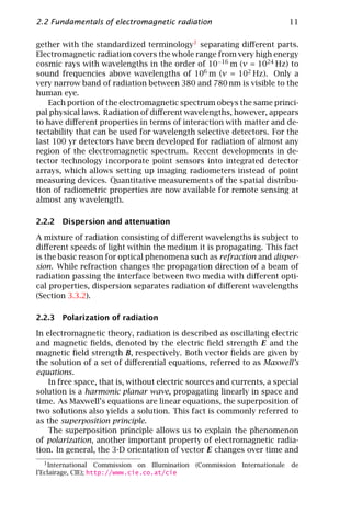
derived from Eq. (2.2)). Silicon (Si) has a bandgap of 1.1 eV and requires
wavelengths below 1.1 µm to be detected. This shows why InSb can
be used as detector material for infrared cameras in the 3-5 µm wave-
length region, while silicon sensors are used for visible radiation. It
also shows, however, that the sensitivity of standard silicon sensors
extends beyond the visible range up to approximately 1 µm, which is
often neglected in applications.
Electromagnetic spectrum. Monochromatic radiation consists of only
one frequency and wavelength. The distribution of radiation over the
range of possible wavelengths is called spectrum or spectral distribu-
tion. Figure 2.1 shows the spectrum of electromagnetic radiation to-](https://image.slidesharecdn.com/computervision-handbookofcomputervisionandapplicationsvolume1-sensorsandimaging-120205081125-phpapp02/85/Computer-vision-handbook-of-computer-vision-and-applications-volume-1-sensors-and-imaging-35-320.jpg)


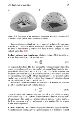


![2.3 Radiometric quantities 21
Extending the point source concept of radiant intensity to extended
sources, the intensity of a surface of finite area can be derived by inte-
grating the radiance over the emitting surface area S:
I(θ, φ) = L(x, θ, φ) cos θ dS (2.22)
S
The infinitesimal surface area dS is given by dS = ds1 ds2 , with the gen-
eralized coordinates s = [s1 , s2 ]T defining the position on the surface.
For planar surfaces these coordinates can be replaced by Cartesian co-
ordinates x = [x, y]T in the plane of the surface.
Total radiant flux. Solving Eq. (2.12) for d2 Φ yields the fraction of
radiant flux emitted from an infinitesimal surface element dS under
the specified direction into the solid angle dΩ
d2 Φ = L(x, θ, φ) cos θ dS dΩ (2.23)
The total flux emitted from the entire surface area S into the hemispher-
ical enclosure H can be derived by integrating over both the surface
area and the solid angle of the hemisphere
2π π /2
Φ= L(x, θ, φ) cos θ dΩ dS = L(x, θ, φ) cos θ sin θ dθ dφ dS
SH S 0 0
(2.24)
Again, spherical coordinates have been used for dΩ and the surface
element dS is given by dS = ds1 ds2 , with the generalized coordinates
s = [s1 , s2 ]T . The flux emitted into a detector occupying only a fraction
of the surrounding hemisphere can be derived from Eq. (2.24) by inte-
grating over the solid angle ΩD subtended by the detector area instead
of the whole hemispheric enclosure H .
Inverse square law. A common rule of thumb for the decrease of ir-
radiance of a surface with distance of the emitting source is the inverse
square law. Solving Eq. (2.11) for dΦ and dividing both sides by the
area dS of the receiving surface, the irradiance of the surface is given
by
dΦ dΩ
E= =I (2.25)
dS dS
For small surface elements dS perpendicular to the line between the
point source and the surface at a distance r from the point source, the](https://image.slidesharecdn.com/computervision-handbookofcomputervisionandapplicationsvolume1-sensorsandimaging-120205081125-phpapp02/85/Computer-vision-handbook-of-computer-vision-and-applications-volume-1-sensors-and-imaging-46-320.jpg)

![2.3 Radiometric quantities 23
The proportionality factor of π shows that the effect of Lambert’s law
is to yield only one-half the exitance, which might be expected for a sur-
face radiating into 2π steradians. For point sources, radiating evenly
into all directions with an intensity I, the proportionality factor would
be 2π . Non-Lambertian surfaces would have proportionality constants
smaller than π .
Another important consequence of Lambert’s cosine law is the fact
that Lambertian surfaces appear to have the same brightness under all
view angles. This seems to be inconsistent with the cosine dependence
of emitted intensity. To resolve this apparent contradiction, radiant
power transfer from an extended source to a detector element with
an area of finite size has to be investigated. This is the basic topic of
radiometry and will be presented in detail in Chapter 5.
It is important to note that Lambert’s cosine law only describes per-
fect radiators or perfect diffusers. It is frequently used to define rules
of thumb, although it is not valid for real radiators in general. For
small angles of incidence, however, Lambert’s law holds for most sur-
faces. With increasing angles of incidence, deviations from the cosine
relationship increase (Section 3.3.3).
2.3.5 Spectral distribution of radiation
So far spectral distribution of radiation has been neglected. Radiative
flux is made up of radiation at a certain wavelength λ or mixtures of
wavelengths, covering fractions of the electromagnetic spectrum with
a certain wavelength distribution. Correspondingly, all derived radio-
metric quantities have certain spectral distributions. A prominent ex-
ample for a spectral distribution is the spectral exitance of a blackbody
given by Planck’s distribution (Section 2.5.1).
Let Q be any radiometric quantity. The subscript λ denotes the cor-
responding spectral quantity Qλ concentrated at a specific wavelength
within an infinitesimal wavelength interval dλ. Mathematically, Qλ is
defined as the derivative of Q with respect to wavelength λ:
∆Q
Qλ = dQλ = lim (2.29)
∆λ→0 ∆λ
The unit of Qλ is given by [·/m] with [·] denoting the unit of the quan-
tity Q. Depending on the spectral range of radiation it sometimes is
more convenient to express the wavelength dependence in units of
[·/µm] (1 µm = 10−6 m) or [·/nm] (1 nm = 10−9 m). Integrated quan-
tities over a specific wavelength range [λ1 , λ2 ] can be derived from](https://image.slidesharecdn.com/computervision-handbookofcomputervisionandapplicationsvolume1-sensorsandimaging-120205081125-phpapp02/85/Computer-vision-handbook-of-computer-vision-and-applications-volume-1-sensors-and-imaging-48-320.jpg)
![24 2 Radiation
spectral distributions by
λ2
λ2
Q λ1 = Qλ dλ (2.30)
λ1
with λ1 = 0 and λ2 = ∞ as a special case. All definitions and relations
derived in Sections 2.3.3 and 2.3.4 can be used for both spectral distri-
butions of radiometric quantities and total quantities, integrated over
the spectral distribution.
2.4 Fundamental concepts of photometry
Photometry relates radiometric quantities to the brightness sensation
of the human eye. Historically, the naked eye was the first device to
measure light and visual perception is still important for designing il-
lumination systems and computing the apparent brightness of sources
and illuminated surfaces.
While radiometry deals with electromagnetic radiation of all wave-
lengths, photometry deals only with the visible portion of the electro-
magnetic spectrum. The human eye is sensitive to radiation between
380 and 780 nm and only radiation within this visible portion of the
spectrum is called “light.”
2.4.1 Spectral response of the human eye
Light is perceived by stimulating the retina after passing the preretinal
optics of the eye. The retina consists of two different types of receptors:
rods and cones. At high levels of irradiance the cones are used to detect
light and to produce the sensation of colors (photopic vision). Rods are
used mainly for night vision at low illumination levels (scotopic vision).
Both types of receptors have different sensitivities to light at different
wavelengths.
The response of the “standard” light-adapted eye is defined by the
normalized photopic spectral luminous efficiency function V (λ) (Fig. 2.9).
It accounts for eye response variation as relates to wavelength and
shows the effectiveness of each wavelength in evoking a brightness sen-
sation. Correspondingly, the scotopic luminous efficiency function V (λ)
defines the spectral response of a dark-adapted human eye (Fig. 2.9).
These curves were formally adopted as standards by the International
Lighting Commission (CIE) in 1924 and 1951, respectively. Tabulated
values can be found in [1, 2, 3, 4, 5]. Both curves are similar in shape.
The peak of the relative spectral luminous efficiency curve for scotopic
vision is shifted to 507 nm compared to the peak at 555 nm for photopic
vision. The two efficiency functions can be thought of as the transfer](https://image.slidesharecdn.com/computervision-handbookofcomputervisionandapplicationsvolume1-sensorsandimaging-120205081125-phpapp02/85/Computer-vision-handbook-of-computer-vision-and-applications-volume-1-sensors-and-imaging-49-320.jpg)
![2.4 Fundamental concepts of photometry 25
Figure 2.9: Spectral luminous efficiency function of the “standard” light-
adapted eye for photopic vision V (λ) and scotopic vision V (λ), respectively.
function of a filter, which approximates the behavior of the human eye
under good and bad lighting conditions, respectively.
As the response of the human eye to radiation depends on a variety
of physiological parameters, differing for individual human observers,
the spectral luminous efficiency function can correspond only to an
average normalized observer. Additional uncertainty arises from the
fact that at intermediate illumination levels both photopic and scotopic
vision are involved. This range is called mesopic vision.
2.4.2 Definition of photometric quantities
In order to convert radiometric quantities to their photometric counter-
parts, absolute values of the spectral luminous efficiency function are
needed instead of relative functions. The relative spectral luminous
efficiency functions for photopic and scotopic vision are normalized to
their peak values, which constitute the quantitative conversion factors.
These values have been repeatedly revised and currently (since 1980)
are assigned the values 683 lm W−1 (lumen/watt) at 555 nm for photopic
vision, and 1754 lm W−1 at 507 nm for scotopic vision, respectively.
The absolute values of the conversion factors are arbitrary numbers
based on the definition of the unit candela (or international standard
candle) as one of the seven base units of the metric system (SI). The
name of this unit still reflects the historical illumination standard: a
candle at a distance of 1 mile observed by the human eye. It is obvious
that this corresponds to the definition of light intensity: a point source
emitting light into a solid angle defined by the aperture of an average
human eye and the squared distance. The current definition of candela
is the luminous intensity of a source emitting monochromatic radiation
of frequency 5.4×10¹⁴ Hz with a radiant intensity of 1/683 W sr−1 [2]. A
practical calibration standard is the primary standard of light adopted](https://image.slidesharecdn.com/computervision-handbookofcomputervisionandapplicationsvolume1-sensorsandimaging-120205081125-phpapp02/85/Computer-vision-handbook-of-computer-vision-and-applications-volume-1-sensors-and-imaging-50-320.jpg)
![26 2 Radiation
in 1918. It defines the candela as luminous intensity in the perpendic-
ular direction of a surface of 1/60 cm2 of a blackbody (Section 2.5.1)
at the temperature of freezing platinum under a pressure of 1013.25
mbar [6, 7].
The conversion from photometric to radiometric quantities reduces
to one simple equation. Given the conversion factors for photopic and
scotopic vision, any (energy-derived) radiometric quantity Qe,λ can be
converted into its photometric counterpart Qν by
780
Qν = 683 lm W−1 Qe,λ V (λ) dλ (2.31)
380
for photopic vision and
780
Qν = 1754 lm W−1 Qe,λ V (λ) dλ (2.32)
380
for scotopic vision, respectively. From this definition it can be con-
cluded that photometric quantities can be derived only from known
spectral distributions of the corresponding radiometric quantities. For
invisible sources emitting radiation below 380 nm or above 780 nm all
photometric quantities are null.
Table 2.2 on page 15 summarizes all basic photometric quantities
together with their definition and units.
Luminous energy and luminous flux. The luminous energy can be
thought of as the portion of radiant energy causing a visual sensation
at the human retina. Radiant energy beyond the visible portion of the
spectrum can also be absorbed by the retina, eventually causing severe
damage to the tissue, but without being visible to the human eye. The
luminous flux defines the total luminous energy per unit time interval
(“luminous power”) emitted from a source or received by a detector.
The units for luminous flux and luminous energy are lm (lumen) and
lm s, respectively.
Luminous exitance and illuminance. Corresponding to radiant exi-
tance and irradiance, the photometric quantities luminous exitance and
illuminance define the luminous flux per unit surface area leaving a
surface or incident on a surface, respectively. As with the radiometric
quantities, they are integrated over the angular distribution of light.
The units of both luminous exitance and illuminance are lm m−2 or lux.
Luminous intensity. Luminous intensity defines the total luminous
flux emitted into unit solid angle under a specified direction. As with its](https://image.slidesharecdn.com/computervision-handbookofcomputervisionandapplicationsvolume1-sensorsandimaging-120205081125-phpapp02/85/Computer-vision-handbook-of-computer-vision-and-applications-volume-1-sensors-and-imaging-51-320.jpg)
![2.4 Fundamental concepts of photometry 27
radiometric counterpart, radiant intensity, it is used mainly to describe
point sources and rays of light. Luminous intensity has the unit lm
sr−1 or candela (cd). For a monochromatic radiation source with Iλ =
I0 δ(λ − 555 nm) and I0 = 1/683 W sr−1 , Eq. (2.31) yields Iν = 1 cd in
correspondence to the definition of candela.
Luminance. Luminance describes the subjective perception of “bright-
ness” because the output of a photometer is proportional to the lumi-
nance of the measured radiation (Chapter 5). It is defined as luminant
flux per unit solid angle per unit projected surface area perpendicular
to the specified direction, corresponding to radiance, its radiometric
equivalent. Luminance is the most versatile photometric quantity, as
all other quantities can be derived by integrating the luminance over
solid angles or surface areas. Luminance has the unit cd m−2 .
2.4.3 Luminous efficacy
Luminous efficacy is used to determine the effectiveness of radiative
or electrical power in producing visible light. The term “efficacy” must
not be confused with “efficiency”. Efficiency is a dimensionless constant
describing the ratio of some energy input to energy output. Luminous
efficacy is not dimensionless and defines the fraction of luminous en-
ergy output able to stimulate the human visual system with respect to
incoming radiation or electrical power. It is an important quantity for
the design of illumination systems.
Radiation luminous efficacy. Radiation luminous efficacy Kr is a mea-
sure of the effectiveness of incident radiation in stimulating the percep-
tion of light in the human eye. It is defined as the ratio of any photo-
metric quantity Qν to the radiometric counterpart Qe integrated over
the entire spectrum of electromagnetic radiation:
∞
Qν
Kr = [lm W−1 ], where Qe = Qe,λ dλ (2.33)
Qe
0
It is important to note that Eq. (2.33) can be evaluated for any radiomet-
ric quantity with the same result for Kr . Substituting Qν in Eq. (2.33)
by Eq. (2.31) and replacing Qe,λ by monochromatic radiation at 555 nm,
that is, Qe,λ = Q0 δ(λ − 555 nm), Kr reaches the value 683 lm W−1 . It
can be easily verified that this is the theoretical maximum luminous
efficacy a beam can have. Any invisible radiation, such as infrared or
ultraviolet radiation, has zero luminous efficacy.
Lighting system luminous efficacy. The lighting system luminous ef-
ficacy Ks of a light source is defined as the ratio of perceptible luminous](https://image.slidesharecdn.com/computervision-handbookofcomputervisionandapplicationsvolume1-sensorsandimaging-120205081125-phpapp02/85/Computer-vision-handbook-of-computer-vision-and-applications-volume-1-sensors-and-imaging-52-320.jpg)
![28 2 Radiation
flux Φν to the total power Pe supplied to the light source:
Φν
Ks = [lm W−1 ] (2.34)
Pe
˜
With the radiant efficiency η = Φe /Pe defining the ratio of total radiative
flux output of an illumination source to the supply power, Eq. (2.34) can
be expressed by the radiation luminous efficacy, Kr :
Φν Φe
Ks = ˜
= Kr η (2.35)
Φe Pe
Because the radiant efficiency of an illumination source is always smaller
than 1, the lighting system luminous efficacy is always smaller than the
radiation luminous efficacy. An extreme example is monochromatic
laser light at a wavelength of 555 nm. Although Kr reaches the max-
imum value of 683 lm W−1 , Ks might be as low as 1 lm W−1 due to the
low efficiency of laser radiation.
2.5 Thermal emission of radiation
All objects at temperatures above absolute zero emit electromagnetic
radiation. This thermal radiation is produced by accelerated electri-
cal charges within the molecular structure of objects. Any accelerated
charged particle is subject to emission of electromagnetic radiation ac-
cording to the Maxwell equations of electromagnetism. A rise in tem-
perature causes an increase in molecular excitation within the mate-
rial accelerating electrical charge carriers. Therefore, radiant exitance
of thermally emitting surfaces increases with the temperature of the
body.
2.5.1 Blackbody radiation
In order to formulate the laws of thermal radiation quantitatively, an
idealized perfect steady-state emitter has been specified. A blackbody
is defined as an ideal body absorbing all radiation incident on it regard-
less of wavelength or angle of incidence. No radiation is reflected from
the surface or passing through the blackbody. Such a body is a perfect
absorber. Kirchhoff demonstrated in 1860 that a good absorber is a
good emitter and, consequently, a perfect absorber is a perfect emitter.
A blackbody, therefore, would emit the maximum possible radiative
flux that any body can radiate at a given kinetic temperature, unless it
contains fluorescent or radioactive materials.
Due to the complex internal structure of matter thermal radiation is
made up of a broad range of wavelengths. However, thermal radiation](https://image.slidesharecdn.com/computervision-handbookofcomputervisionandapplicationsvolume1-sensorsandimaging-120205081125-phpapp02/85/Computer-vision-handbook-of-computer-vision-and-applications-volume-1-sensors-and-imaging-53-320.jpg)
![2.5 Thermal emission of radiation 29
emitted from incandescent objects obeys the same laws as thermal ra-
diation emitted from cold objects at room temperature and below. In
1900, Max Planck theoretically derived the fundamental relationship
between the spectral distribution of thermal radiation and tempera-
ture [8]. He found that the spectral radiance of a perfect emitter at
absolute temperature T is given by
−1
2hc 2 ch
Le,λ (T ) = exp −1 (2.36)
λ5 kB λT
−1
2c ch
Lp,λ (λ, T ) = exp −1 (2.37)
λ4 kB λT
with
h = 6.6256 × 10⁻³⁴ J s Planck’s constant
kB = 1.3805 × 10⁻²³ J K−1 Boltzmann constant (2.38)
c = 2.9979 × 10⁸ m s−1 speed of light in vacuum
The photon-related radiance of a blackbody Lp,λ (T ) is obtained by di-
viding the energy related radiance Le,λ (T ) by the photon energy ep as
given by Eq. (2.2). Detailed derivations of Planck’s law can be found in
[7, 9, 10].
Although the assumption of a perfect emitter seems to restrict the
practical usage, Planck’s law proves useful to describe a broad range of
thermally emitting objects. Sources like the sun, incandescent lamps,
or—at much lower temperatures—water and human skin have black-
body-like emission spectra. The exact analytical form of blackbody
radiation is an invaluable prerequisite for absolute radiometric calibra-
tion standards.
Figure 2.10 shows several Planck distributions for different temper-
atures. As already pointed out at the beginning of this chapter, the
shapes of energy-derived and photon-derived quantities deviate from
each other due to the conversion from photon energy into photon num-
ber. It is also of interest to note that a single generalized blackbody
radiation curve may be drawn for the combined parameter λT , which
can be used for determining spectral exitance at any wavelength and
temperature. Figure 2.11a shows this curve as fractional exitance rel-
ative to the peak value, plotted as a function of λT . The fraction of
the total exitance lying below any given value of λT is also shown. An
interesting feature of Planck’s curve is the fact that exactly one-fourth
of the exitance is radiated below the peak value.
In Fig. 2.11b the solar irradiance above the earth’s atmosphere is
plotted together with the exitance of a blackbody at T = 6000 K, which
corresponds to the temperature of the solar surface (Section 6.2.1).](https://image.slidesharecdn.com/computervision-handbookofcomputervisionandapplicationsvolume1-sensorsandimaging-120205081125-phpapp02/85/Computer-vision-handbook-of-computer-vision-and-applications-volume-1-sensors-and-imaging-54-320.jpg)
![30 2 Radiation
a
9
10
6400 K
7
10 3200 K
Me,l (T) [Wm ]
-2
5 1600 K
10
3 800 K
10
400 K
1
visible
10 200 K
-1 100 K
10
-3
10
0.1 1 10 100 1000
l m [ m]
b
30
10
visible 6400 K
26
10 3200 K
1600 K
Mp,l (T) [Wm ]
-2
22
10 800 K
400 K
18
10 200 K
100 K
14
10
10
10
4 6
0.01 1 100 10 10
l m [ m]
Figure 2.10: a Spectral energy-derived exitance of a blackbody vs wavelength
at temperatures from 100 K-6400 K. b Spectral photon-derived exitance of a
blackbody at the same temperatures.
2.5.2 Properties of Planck’s distribution
Angular Distribution. A blackbody, by definition, radiates uniformly
in angle. The radiance of a blackbody surface is independent of view
angle, that is, Lλ (T , θ, φ) = Lλ (T ). This surface property is called Lam-
bertian (Section 2.3.4). Therefore, blackbody radiation is fully specified
by the surface temperature T . All radiometric quantities can be de-
rived from the spectral radiance distributions, Eq. (2.36) or Eq. (2.37),
as outlined in Section 2.3.4. An important example is the spectral ra-
diant exitance of a blackbody Mλ (T ), which is simply given by π Lλ (T )
because a blackbody, by definition, has a Lambertian surface:
−1
2π hc 2 ch
Me,λ (T ) = exp −1 (2.39)
λ5 kB λT
−1
2π c ch
Mp,λ (T ) = exp −1 (2.40)
λ4 kB λT](https://image.slidesharecdn.com/computervision-handbookofcomputervisionandapplicationsvolume1-sensorsandimaging-120205081125-phpapp02/85/Computer-vision-handbook-of-computer-vision-and-applications-volume-1-sensors-and-imaging-55-320.jpg)


![2.5 Thermal emission of radiation 33
λ T [µm°K]
3x10 2 3x10 3 3x10 4 3x10 5 3x10 6
10
7.5
Rayleigh-Jeans
5
deviation [ %]
2.5
Planck
0
-2.5
Wien
-5
-7.5
-10
1 10. 100. 1000. 10000.
wavelength λ λ µ µm] ö (at T = 300 K)
[ °
Figure 2.12: Deviation of Wien’s radiation law and Rayleigh-Jeans law from
the exact Planck distribution.
Rayleigh-Jeans law. For large values of λT hc/kB an approximate
solution can be found by expanding the exponential factor of Eq. (2.36)
in a Taylor series
2 −1
2hc 2 ch 1 ch
Le,λ (T ) = + + ··· (2.47)
λ5 kB λT 2 kB λT
Disregarding all terms of second and higher order in Eq. (2.47) yields
the Rayleigh-Jeans law
2ckB
Le,λ (T ) = T (2.48)
λ4
This law is a good approximation of the decrease of Le,λ (T ) at large
wavelengths. At small wavelengths the predicted exitance approaches
infinity, which is known as the UV catastrophe (Fig. 2.12).
2.5.4 Luminous efficacy of blackbody radiation
An important quantity of an incandescent object used as illumination
source is the radiation luminous efficacy Kr . Replacing Qν in Eq. (2.33)
by the blackbody luminous exitance Mν (T ) computed from Eq. (2.31)
with Eq. (2.39) and using the Stefan-Boltzmann law Eq. (2.41) yields
780
683
Kr (T ) = Mλ (T )V (λ)dλ [lm W−1 ] (2.49)
σT4
380
Figure 2.13 shows Kr for a temperature range from 2000 K to 40,000 K.
For temperatures up to 2000 K the radiant luminous efficacy lies well](https://image.slidesharecdn.com/computervision-handbookofcomputervisionandapplicationsvolume1-sensorsandimaging-120205081125-phpapp02/85/Computer-vision-handbook-of-computer-vision-and-applications-volume-1-sensors-and-imaging-58-320.jpg)
![34 2 Radiation
100
50
20
K r(T)
10
5
2
2 5 6.6 10 20 40
T [K] x 103
Figure 2.13: Radiation luminous efficacy of a blackbody vs temperature T .
below 1 lm W−1 . This shows that typical incandescent lamps with tem-
peratures below 2000 K are very inefficient illumination sources. Most
of the energy is emitted in the IR region. The peak of the radiation lu-
minous efficacy of blackbody radiation lies at 6600 K which is close to
the surface temperature of the sun. This demonstrates how the human
visual system has adapted to the solar spectrum by evolution.
2.6 Acoustic waves
Although it does not belong to electromagnetic radiation, ultrasound
is gaining increasing importance in acoustic imaging applications such
as medical imaging. With improved detector performance resolutions
of less than 1 mm can be achieved. The major advantage of ultrasound
is its performance in penetrating opaque objects, rigid bodies, as well
as fluid systems, in a nondestructive way. Prominent examples are
material research and medical diagnostics
Ultrasound consists of acoustic waves with frequencies between
15 kHz and 10 GHz (1010 Hz). It is generated by electroacoustical trans-
ducers such as piezoelectric crystals at resonant frequencies. The low-
est eigenfrequency of a Piezo quartz plate of thickness l is given by
ν0 = cq /2l (2.50)
where cq = 5.6 × 105 cm s−1 is the speed of sound in quartz. The spec-
trum of emitted frequencies consists of integer multiples of ν0 .
In contrast to electromagnetic waves, acoustic waves need a carrier.
They travel with the speed of sound in the carrier medium, which is
given by
cm = (ρ0 βad )−1/2 (2.51)](https://image.slidesharecdn.com/computervision-handbookofcomputervisionandapplicationsvolume1-sensorsandimaging-120205081125-phpapp02/85/Computer-vision-handbook-of-computer-vision-and-applications-volume-1-sensors-and-imaging-59-320.jpg)
![2.7 References 35
where ρ0 is the static density and βad the adiabatic compressibility:
1 ∂V
βad = − (2.52)
V ∂P
It is given as the relative volume change caused by a uniform pressure
without heat exchange. As the speed of acoustic waves cm depends
only on the elastic properties of the medium, acoustic waves of all fre-
quencies travel with the same speed. Thus, acoustic waves show no dis-
persion. This important feature is used in acoustic imaging techniques
to measure the density of the medium by run length measurements of
ultrasonic reflexes.
Equation (2.51) is only valid for longitudinal waves caused by iso-
tropic pressure with deformation in the direction of propagation. Due
to the internal structure of solids the propagation of sound waves is
no longer isotropic and shear forces give rise to transversal acoustic
waves.
2.7 References
[1] Oriel Corporation, (1994). Light Sources, Monochromators & Spectro-
graphs, Detectors & Detection Systems, Fiber Optics, Vol. II. Stratford,
CT: Oriel Corporation.
[2] CIE, (1983). The Basis of Physical Photometry. Technical Report.
[3] Kaufman, J. E. (ed.), (1984). IES Lighting Handbook—Reference Volume.
New York: Illuminating Engineering Society of North America.
[4] Laurin Publishing, (1998). The Photonics Design and Applications Hand-
book, 44th edition. Pittsfield, MA: Laurin Publishing CO.
[5] McCluney, W. R., (1994). Introduction to Radiometry and Photometry.
Boston: Artech House.
[6] Walsh, J. W. T. (ed.), (1965). Photometry, 3rd edition. New York: Dover.
[7] Wolfe, W. L. and Zissis, G. J. (eds.), (1989). The Infrared Handbook, 3rd
edition. Michigan: The Infrared Information Analysis (IRIA) Center, Envi-
ronmental Research Institute of Michigan.
[8] Planck, M., (1901). Ann. Phys., 4(3):p. 553.
[9] Dereniak, E. L. and Boreman, G. D., (1996). Infrared Detectors and Systems.
New York: John Wiley & Sons, Inc.
[10] Planck, M., (1991). The Theory of Heat Radiation. New York: Dover.](https://image.slidesharecdn.com/computervision-handbookofcomputervisionandapplicationsvolume1-sensorsandimaging-120205081125-phpapp02/85/Computer-vision-handbook-of-computer-vision-and-applications-volume-1-sensors-and-imaging-60-320.jpg)


![40 3 Interaction of Radiation with Matter
˜ ˜ ˜
Emissivity The forementioned quantities ρ, α, and τ define the prop-
erty of passive receivers in modifying incident radiative flux. The
emissivity or emittance ˜ quantifies the performance of an actively
radiating object compared to a blackbody, which provides the upper
limit of the spectral exitance of a source. It is defined by the ratio
of the exitances,
Ms (T )
˜= (3.4)
Mb (T )
where Ms and Mb denote the exitance of the emitting source, and
the exitance of the blackbody at the temperature T , respectively. As
a blackbody has the maximum possible exitance of an object at the
given temperature, ˜ is always smaller than 1.
3.2.2 Spectral and directional dependencies
All of the foregoing introduced quantities can have strong variations
with direction, wavelength, and polarization state that have to be spec-
ified in order to measure the optical properties of an object. The emis-
sivity of surfaces usually only slightly decreases for angles of up to 50°
and rapidly falls off for angles larger than 60°; it approaches zero for
90° [1]. The reflectivity shows the inverse behavior.
To account for these dependencies, we define the spectral direc-
tional emissivity ˜(λ, θ, φ) as ratio of the source spectral radiance Lλ,s
to the spectral radiance of a blackbody Lλ,b at the same temperature T :
Lλ,s (θ, φ, T )
˜(λ, θ, φ) = (3.5)
Lλ,b (θ, φ, T )
The spectral hemispherical emissivity ˜(λ) is similarly given by the ra-
diant exitance of the source and a blackbody at the same temperature,
T:
Mλ,s (T )
˜(λ) = (3.6)
Mλ,b (T )
Correspondingly, we can define the spectral directional reflectivity,
the spectral directional absorptivity, and the spectral directional trans-
missivity as functions of direction and wavelength. In order to simplify
notation, the symbols are restricted to ρ, α, τ and ˜ without further in-
˜ ˜ ˜
dices. Spectral and/or directional dependencies will be indicated by
the variables and are mentioned in the text.](https://image.slidesharecdn.com/computervision-handbookofcomputervisionandapplicationsvolume1-sensorsandimaging-120205081125-phpapp02/85/Computer-vision-handbook-of-computer-vision-and-applications-volume-1-sensors-and-imaging-65-320.jpg)
![3.2 Basic definitions and terminology 41
3.2.3 Terminology conventions
Emission, transmission, reflection, and absorption of radiation either
refer to surfaces and interfaces between objects or to the net effect
of extended objects of finite thickness. In accordance with Siegel and
Howell [2] and McCluney [3] we assign the suffix -ivity to surface-related
(intrinsic) material properties and the suffix -ance to volume-related
(extrinsic) object properties. To reduce the number of equations we
exclusively use the symbols ˜, α, ρ and τ for both types. If not further
˜ ˜ ˜
specified, surface- and volume-related properties can be differentiated
by the suffixes -ivity and -ance, respectively. More detailed definitions
can be found in the CIE International Lighting Vocabulary [4].
3.2.4 Spectral selectivity
For most applications the spectral optical properties have to be related
to the spectral sensitivity of the detector system or the spectral distri-
˜
bution of the radiation source. Let p(λ) be any of the following material
properties: α, ρ, τ , or ˜. The spectral selective optical properties ps can
˜ ˜ ˜ ˜
be defined by integrating the corresponding spectral optical property
˜
p(λ) over the entire spectrum, weighted by a spectral window function
w(λ):
∞
˜
w(λ)p(λ)dλ
0
˜
ps = ∞ (3.7)
w(λ) dλ
0
Examples of spectral selective quantities include the photopic lumi-
nous transmittance or reflectance for w(λ) = V (λ) (Chapter 2), the
solar transmittance, reflectance, or absorptance for w(λ) = Eλ,s (so-
lar irradiance), and the emittance of an object at temperature T for
˜
w(λ) = Eλ,b (T ) (blackbody irradiance). The total quantities p can be
˜
obtained by integrating p(λ) over all wavelengths without weighting.
3.2.5 Kirchhoff’s law
Consider a body that is in thermodynamic equilibrium with its sur-
rounding environment. Conservation of energy requires Φi = Φa + Φr +
Φt and, therefore,
˜ ˜ ˜
α+ρ+τ =1 (3.8)](https://image.slidesharecdn.com/computervision-handbookofcomputervisionandapplicationsvolume1-sensorsandimaging-120205081125-phpapp02/85/Computer-vision-handbook-of-computer-vision-and-applications-volume-1-sensors-and-imaging-66-320.jpg)
![42 3 Interaction of Radiation with Matter
Table 3.1: Basic (idealized) object and surface types
Object Properties Description
Opaque ˜
˜(λ) + ρ(λ) = 1, Cannot be penetrated by radiation. All exi-
body ˜
τ (λ) = 0 tant radiation is either reflected or emitted.
AR coating ˜
˜(λ) + τ (λ) = 1, No radiation is reflected at the surface. All
˜
ρ(λ) = 0 exitant radiation is transmitted or emitted.
Ideal ˜
˜(λ) = ρ(λ) = 0, All radiation passes without attenuation.
window ˜
τ (λ) = 1 The temperature is not accessible by IR
thermography because no thermal emission
takes place.
Mirror ˜
˜(λ) = τ (λ) = 0, All incident radiation is reflected. The tem-
˜
ρ(λ) = 1 perature is not accessible by IR thermo-
graphy because no thermal emission takes
place.
Blackbody ˜ ˜
τ (λ) = ρ(λ) = 0, All incident radiation is absorbed. It has the
˜(λ) = ˜ = 1 maximum possible exitance of all objects.
Graybody ˜(λ) = ˜ < 1, Opaque object with wavelength independent
˜
ρ(λ) = 1 − ˜, emissivity. Same spectral radiance as a
˜
τ (λ) = 0 blackbody but reduced by the factor ˜.
In order to maintain equilibrium, the emitted flux must equal the ab-
sorbed flux at each wavelength and in each direction. Thus
˜
α(λ, θ, φ) = ˜(λ, θ, φ) (3.9)
This relation is known as Kirchhoff’s law [5]. It also holds for the in-
tegrated quantities ˜(λ) and ˜. Kirchoff’s law does not hold for active
optical effects shifting energy between wavelengths, such as fluores-
cence, or if thermodynamic equilibrium is not reached. Kirchhoff’s law
also does not apply generally for two different components of polar-
ization [6, 7].
Table 3.1 summarizes basic idealized object and surface types in
terms of the optical properties defined in this section. Real objects
and surfaces can be considered a mixture of these types. Although
the ideal cases usually do not exist for the entire spectrum, they can
be realized for selective wavelengths. Surface coatings, such as, for
example, anti-reflection (AR) coatings, can be technically produced with
high precision for a narrow spectral region.
Figure 3.3 shows how radiometric measurements are influenced by
the optical properties of objects. In order to measure the emitted flux
Φ1 (e. g., to estimate the temperature of the object), the remaining seven
quantities ˜1 , ˜2 , ˜3 , ρ1 , τ1 , Φ2 , and Φ3 have to be known. Only for a
˜ ˜
blackbody is the total received flux the flux emitted from the object of
interest.](https://image.slidesharecdn.com/computervision-handbookofcomputervisionandapplicationsvolume1-sensorsandimaging-120205081125-phpapp02/85/Computer-vision-handbook-of-computer-vision-and-applications-volume-1-sensors-and-imaging-67-320.jpg)

![44 3 Interaction of Radiation with Matter
a
3 5
3 0
]-2
2 5
m
ε= 1
(3 0 0 K ) [W
2 0
1 5 ε= 0 . 6
e ,λ
1 0
5 ε = ε( λ)
M
0
0 5 1 0 1 5 2 0 2 5 3 0
λ [ µm ]
b
1.0 1.0
Mb(λ,T), Eb(λ,T) (normalized)
white paint
reflectance ~
ρ
T = 29 ission
T = 60 iance
00 K
3K
0.1 0.5
al em
rad
solar ir
therm
aluminum
0.0 0.0
0.1 0.5 1 5 10 50
λ [µm]
Figure 3.4: a Spectral exitance of a blackbody, a graybody, and a selective
emitter at the same temperature. b Spectral solar irradiance and spectral ther-
mal exitance of a blackbody at ambient temperature vs spectral emissivity of
aluminum and white paint, respectively (schematic).
the same spectral shape as the same radiometric quantity of blackbod-
ies, multiplied by the constant factor ˜ (Fig. 3.4a). Graybodies do not
necessarily have to be gray. They appear to have the same color as a
blackbody at the same temperature but have a lower total exitance:
Mλ,g (T ) = ˜σ T 4 (3.12)
A surface is called nonblackbody if the emissivity varies with wave-
length. Such a surface is the general case and is also called selective
emitter (Fig. 3.4a). Tabulated values of ˜ for common surface materials
can be found in [3, 7].
Example 3.1: Infrared thermography
The temperature T of objects can be measured remotely by infrared
thermography (Section 2.5, and Volume 3, Chapter 35). As already
pointed out in Section 3.2, the fraction (1 − ˜) of the total exitance
originates from the environment biasing the temperature measure-
ment. The measured total exitance is interpreted to originate from](https://image.slidesharecdn.com/computervision-handbookofcomputervisionandapplicationsvolume1-sensorsandimaging-120205081125-phpapp02/85/Computer-vision-handbook-of-computer-vision-and-applications-volume-1-sensors-and-imaging-69-320.jpg)
![3.3 Properties related to interfaces and surfaces 45
a blackbody at the apparent temperature T . Assuming an isother-
mal environment at blackbody temperature Te , the temperatures are
related by the Stefan-Boltzmann law Eq. (2.41):
4
σT = ˜σ T 4 + (1 − ˜)σ Te
4
(3.13)
In the limit of small temperature differences between environment
and the body of interest (Te − T T ), Eq. (3.13) can be approximated
by [8]
T ≈ ˜T + (1 − ˜)Te or T − T = (1 − ˜)(Te − T ) (3.14)
This simplified estimation gives a rule of thumb for errors associated
with low emissivity. A 1 % deviation of from unity results in a 0.01 K
temperature error per 1 K difference of object and ambient temper-
ature. Although this is a simplified computation, it can be used to
estimate the influence of ambient temperature on thermography of
nonblackbodies. If the ambient temperature and the emissivity of the
object are known, this error can be corrected according to Eq. (3.13).
In this context it has to be pointed out that radiation from the en-
vironment can also originate from the cooled CCD detector of an IR
camera itself being reflected from the object of interest. As IR de-
tectors usually operate at liquid nitrogen temperature (75 K), errors
in the temperature measurement in the order of 2 K can occur even
for a very high emissivity of ˜ = 0.99! Uncooled infrared imagers can
reduce this type of error.
Example 3.2: Solar absorbers
A solar absorber has to be designed in such a way that as much so-
lar irradiance as possible is collected without emitting the collected
energy by thermal radiation. The absorber has to be covered with a
coating that has a high absorptivity and, correspondingly, a high emis-
sivity over the solar spectrum and a low emissivity over the longwave
IR portion of the spectrum.
Example 3.3: Solar emitters
An aircraft painting needs to be a solar emitter . In order to reduce
thermal heating and relieve air conditioning requirements during
ground-based operations, the solar irradiance has to be reflected as
much as possible. The absorptivity over the solar spectrum, there-
fore, has to be as low as possible. According to Fig. 3.4b this can be
˜
achieved by either white paint (TiO2 , α(0.5 µm) = 0.19 [7]) or polished
˜
aluminum (α(0.5 µm) = 0.19 [7]). Because an aircraft is made from
aluminum, the surfaces used to be finished by the blank aluminum.
Aluminum, however, remains at low emissivity over the entire IR por-
tion of the spectrum (˜(10 µm) = 0.05 [3]; refer to Fig. 3.4b). Any
solar energy that is not reflected heats up the plane and has to be
emitted in the IR with maximum emissive power near 10 µm. White
paint has a much higher emissivity in this portion of the spectrum
(TiO2 , ˜(10 µm) = 0.94 [9]), so white-painted surfaces remain up to](https://image.slidesharecdn.com/computervision-handbookofcomputervisionandapplicationsvolume1-sensorsandimaging-120205081125-phpapp02/85/Computer-vision-handbook-of-computer-vision-and-applications-volume-1-sensors-and-imaging-70-320.jpg)
![46 3 Interaction of Radiation with Matter
surface
normal
ra ed
in ay
y
r
cid
ct
fle
en
Φi
re
t
θ1 θ1 Φr
n1
n2 > n1
Φ (z) Φt
refr ray
θ2
acte
d
Figure 3.5: Refraction and specular reflection at interfaces.
19 K cooler under direct sunlight exposure than aluminum surfaces
[10, 11]. Airline operators paint fuselage tops white today, rather
than leaving their aluminum surface shiny.
3.3.2 Refraction
The real part n(λ) of the complex index of refraction N Eq. (3.10) con-
stitutes the index of refraction of geometric optics, that is, the ratio of
the speed of light in a vacuum to the speed of light in a medium under
consideration. It determines the change in the direction of propaga-
tion of radiation passing the interface of two materials with different
dielectric properties. According to Snell’s law, the angles of incidence
θ1 and refraction θ2 are related by (Fig. 3.5)
sin θ1 n2
= (3.15)
sin θ2 n1
where n1 and n2 are the indices of refraction of the two materials. It is
the basis for transparent optical elements, such as lenses and prisms
(Chapter 4). While prisms make use of the wavelength dependence of
refraction to separate radiation of different wavelengths, lenses suffer
from this effect (chromatic aberration).
3.3.3 Specular reflection
The direction of incident ray, reflected ray, and the surface normal vec-
tor span the plane of incidence perpendicular to the surface of reflec-
tion (Fig. 3.5). At smooth interfaces between two materials with dif-
ferent dielectric properties specular reflection occurs. The angles of
incidence and reflection are equal (Fig. 3.6a).
˜
The reflectivity, ρ, of a surface is defined as the ratio between in-
cident and reflected flux. It depends on the indices of refraction of
the two materials, the angle of incidence, and the polarization of the](https://image.slidesharecdn.com/computervision-handbookofcomputervisionandapplicationsvolume1-sensorsandimaging-120205081125-phpapp02/85/Computer-vision-handbook-of-computer-vision-and-applications-volume-1-sensors-and-imaging-71-320.jpg)
![3.3 Properties related to interfaces and surfaces 47
a b c
θi θr
Figure 3.6: a Specular, b diffuse, c and subsurface reflection at interfaces.
a b
1.0 1.0 ||
||
Transmissivity
θc = 41.24° (n = 1.517)
0.8 ⊥ 0.8 Transmissivity ⊥
critical angle of
total reflection
0.6 0.6
0.4 0.4
0.2 ⊥ 0.2 ⊥
Reflectivity Reflectivity
|| ||
0.0 0.0
0 10 20 30 40 50 60 70 80 90 0 10 20 30 40 50 60 70 80 90
Figure 3.7: Reflectivities and transmissivities vs angle of incidence for parallel
( ) and perpendicular (⊥) polarized light at the interface between air (n1 = 1.0)
and BK7 glass (n2 = 1.517). a Transition air to glass. b Transition glass to
air. The shaded area shows angles beyond the critical angle of total internal
reflection.
radiation. The specular reflectivities of the polarization components
parallel ( ) and perpendicular (⊥) to the plane of incidence are given by
Fresnel’s equations [12]:
tan2 (θ1 − θ2 ) sin2 (θ1 − θ2 ) ˜ ˜
ρ + ρ⊥
˜
ρ = , ˜
ρ⊥ = , ˜
and ρ = (3.16)
tan2 (θ1 + θ2 ) 2
sin (θ1 + θ2 ) 2
˜
where the total reflectivity for unpolarized radiation ρ is the average
(arithmetic mean) of the two polarization components. The angles θ1
and θ2 are the angles of incidence and refraction in the medium, which
are related by Snell’s law, Eq. (3.15). Figure 3.7 shows the angular de-
pendence of Eq. (3.16) for the transition from BK7 glass to air and vice
versa.
From Fresnel’s equations three important properties of specular re-
flection at object interfaces can be inferred (Fig. 3.7):
1. Parallel polarized light is not reflected at all at a certain angle, called
the polarizing or Brewster angle θb . At this angle the reflected and](https://image.slidesharecdn.com/computervision-handbookofcomputervisionandapplicationsvolume1-sensorsandimaging-120205081125-phpapp02/85/Computer-vision-handbook-of-computer-vision-and-applications-volume-1-sensors-and-imaging-72-320.jpg)
![48 3 Interaction of Radiation with Matter
refracted rays are perpendicular to each other [12]:
1
θb = arcsin (3.17)
1 + n2 /n2
1 2
2. At the transition from the medium with higher refractive index to
the medium with lower refractive index, there is a critical angle θc
n1
θc = arcsin , with n1 < n 2 (3.18)
n2
beyond which all light is reflected back into the medium of origin.
At this angle Snell’s law would produce an angle of refraction of 90°.
The reflectivity is unity for all angles of incidence greater than θc ,
which is known as total internal reflection and used in light conduc-
tors and fiber optics.
3. At large (grazing) angles, object surfaces have a high reflectivity,
independent from n. Therefore, objects usually deviate from an
ideal Lambertian reflector for large angles of incidence.
At normal incidence (θ = 0) there is no difference between perpen-
dicular and parallel polarization and
(n1 − n2 )2 (n − 1)2 n1
˜
ρ= 2
= , with n= (3.19)
(n1 + n2 ) (n + 1)2 n2
Note that Eqs. (3.16) and (3.19) are only exact solutions for transparent
dielectric objects (Section 3.4) with small imaginary parts, k, of the com-
plex refractive index N, Eq. (3.10): k 1. For non-negligible imaginary
parts the normal reflectivity Eq. (3.19) has to be modified:
(n1 − n2 )2 + k2
˜
ρ= (3.20)
(n1 + n2 )2 + k2
The wavelength dependence of the refractive index can change the
spectral composition of radiation by reflection. Silver (Ag) has a high
reflectivity above 0.9 over the entire visible spectrum. The reflectivity
of Gold (Au) also lies above 0.9 for wavelengths beyond 600 nm, but
shows a sudden decrease to 0.4 for wavelengths below 500 nm. This
increased absorption of blue light compared to red light is responsible
for the reddish appearance of gold surfaces in contrast to the white
metallic glare of silver surfaces.
3.3.4 Diffuse reflection
Very few materials have pure specular surface reflectivity. Most sur-
faces show a mixture of matte and specular reflection. As soon as sur-
face microroughness has the same scale as the wavelength of radiation,](https://image.slidesharecdn.com/computervision-handbookofcomputervisionandapplicationsvolume1-sensorsandimaging-120205081125-phpapp02/85/Computer-vision-handbook-of-computer-vision-and-applications-volume-1-sensors-and-imaging-73-320.jpg)
![3.3 Properties related to interfaces and surfaces 49
dΩr
dΩi
θr
θi
dS
φr
φi
Figure 3.8: Illustration of the angles used in the definition of the bidirectional
reflectivity distribution function (BRDF).
diffraction at the microstructures occurs. At larger scales, microfacets
with randomly distributed slopes relative to the surface normal are re-
flecting incident light in various directions (Fig. 3.6b). Depending on
the size and slope distribution of the microroughness, these surfaces
have a great variety of reflectivity distributions ranging from isotropic
(Lambertian) to strong forward reflection, where the main direction is
still the angle of specular reflection. An excellent introduction into light
scattering and surface roughness is provided by Bennet and Mattsson
[13].
A mixture of specular and diffuse reflection can also be caused by
subsurface scattering of radiation, which is no longer a pure surface-
related property. Radiation penetrating a partially transparent object
can be scattered at optical inhomogeneities (Section 3.4) and leave the
object to cause diffuse reflection (Fig. 3.6c). Reflected light from below
the surface is subject to bulk related interactions of radiation with mat-
ter that can change the spectral composition of radiation before it is
re-emitted. For this reason, diffusely scattered light shows the colors of
objects while highlights of specular reflections usually show the color
of the incident light, which is white for ambient daylight.
In order to describe quantitatively the angular reflectivity distribu-
tion of arbitrary objects, the bidirectional reflectivity distribution func-
tion (BRDF), f , is used (Fig. 3.8). It is a function of the spherical angles
of incidence (θi , φi ) and reflection (θr , φr ), and defines the ratio of re-
flected radiance Lr to the incident irradiance Ei of the reflecting surface
[7]:
Lr (θr , φr )
f (θi , φi , θr , φr ) = (3.21)
Ei (θi , φi )
This definition accounts for the fact that an optical system measures
the radiance leaving a surface while distribution of incident radiation](https://image.slidesharecdn.com/computervision-handbookofcomputervisionandapplicationsvolume1-sensorsandimaging-120205081125-phpapp02/85/Computer-vision-handbook-of-computer-vision-and-applications-volume-1-sensors-and-imaging-74-320.jpg)
![50 3 Interaction of Radiation with Matter
a b c
Figure 3.9: Spheres shaded using the Phong illumination model: a ambient
reflection, b diffuse reflection, and c specular reflection. (By C. Garbe, University
of Heidelberg.)
is quantified by the surface irradiance. The two extreme cases are spec-
ular and Lambertian surfaces. A purely specular surface has a nonzero
˜
value only for θi = θr and φi = φr so that f = ρδ(θi − θr )δ(φi − φr ).
A Lambertian surface has no dependence on angle, and a flat surface
therefore has f = ρπ −1 . The hemispherical reflectivity in each case is
˜
˜
ρ.
3.3.5 Reflection models in computer graphics
A major task of computer graphics is the realistic visualization of ob-
ject surfaces incorporating material properties. A number of illumina-
tion models, called lighting models or shading models, have been de-
veloped for photorealistic rendering. Graphics researchers have often
approximated the underlying rules of radiation theory either to sim-
plify computation or because more accurate models were not known in
the graphics community [14].
A physically motivated model has been introduced by Cook and Tor-
rance [15], incorporating the surface roughness by microfacets with a
certain probability distribution around the normal of the macroscopic
surface. The internal complexity, however, prevents this approach
from common usage in real-time computer graphics.
For practical usage an illumination model has become standard in
computer graphics, assuming reflection to be a mixture of ambient,
diffuse (Lambertian), and specular reflection. It can be implemented
very efficiently and allows adaptation to most natural surface proper-
ties with good agreement to physical models1 .
1 To stay consistent with radiometric notation, we replace the computer graphics
˜
symbols for reflectivity kx by ρx and replace the color coefficient Ox,λ by using a spec-
˜
tral reflectivity ρx,λ . The subscript x denotes one of the indices a, d, and s for ambient,
diffuse, and specular reflection. It also has to be pointed out that the term intensity is
frequently used for the apparent brightness of a surface in computer graphics. As the
brightness of a surface corresponds to the radiometric term radiance (Section 2.3.3) we
use the term radiance exclusively.](https://image.slidesharecdn.com/computervision-handbookofcomputervisionandapplicationsvolume1-sensorsandimaging-120205081125-phpapp02/85/Computer-vision-handbook-of-computer-vision-and-applications-volume-1-sensors-and-imaging-75-320.jpg)
![3.3 Properties related to interfaces and surfaces 51
n
l r
v
θ θ
α
Figure 3.10: Reflection at surfaces: Direction to light source ¯ surface normal
l
¯ ¯ ¯
vector n, direction of specular reflection r direction to the viewer, v .
Ambient reflection. The most simple approach assumes ambient light ,
with a spectral intensity Iaλ , impinging equally on all surfaces from all
directions. The reflected spectral radiance Laλ of such a surface will be
independent from viewing direction:
˜
Laλ = Iaλ ρaλ (3.22)
˜
where ρaλ is the spectral ambient reflection coefficient . It is a material
property that does not necessarily correspond to the physical reflec-
tivity of the material. A surface rendered according to Eq. (3.22) will
˜
appear flat with a homogeneous brightness if ρaλ remains constant
over the object surface (Fig. 3.9a).
Diffuse reflection. For a perfectly diffuse (Lambertian) surface the re-
flected radiance Ldλ does not depend on the angle of reflection. If a
Lambertian surface is illuminated by a point light source with intensity
Ipλ , the surface irradiance will vary with the cosine of the angle of inci-
dence θ, which can be replaced by the inner vector product nT ¯ of the
¯ l
surface normal n and the normalized direction of incidence ¯ (Fig. 3.10).
¯ l
Thus,
Ldλ = fp Ipλ ρdλ cos θ = fp Ipλ ρdλ nT ¯
˜ ˜ ¯ l (3.23)
˜
where ρdλ is the diffuse reflection coefficient and fp defines the light
source attenuation factor accounting for the distance d of the point
source. A common practice is to set fp = 1/d2 according to the inverse
square law Eq. (2.26). Refined models use an inverse second-order poly-
nomial [14]. Objects rendered according to Eq. (3.23) appear to have
been illuminated by a flashlight in a dark room (Fig. 3.9b).
Specular reflection. A popular illumination model for nonperfect re-
flectors was developed by Phong [16]. The Phong illumination model
assumes that maximum reflectance occurs when the angle α between
¯ ¯
the direction of specular reflection r and the viewing direction v is](https://image.slidesharecdn.com/computervision-handbookofcomputervisionandapplicationsvolume1-sensorsandimaging-120205081125-phpapp02/85/Computer-vision-handbook-of-computer-vision-and-applications-volume-1-sensors-and-imaging-76-320.jpg)
![52 3 Interaction of Radiation with Matter
zero and falls off sharply with increasing α (Fig. 3.10). The falloff is
approximated by cosn α with the specular reflection exponent n. This
complies with the fact that the BRDF f of Eq. (3.21) can be approxi-
mated by a power of cosine for most surfaces. For a point light source
with intensity Ipλ , the reflected radiance Lsλ in this model is given by
n
Lsλ = fp Ipλ ρsλ (θ) cosn α = fp Ipλ ρsλ r T n
˜ ˜ ¯ ¯ (3.24)
˜
where the specular reflection coefficient ρsλ depends on the angular re-
flectivity distribution of specular reflection. It is, however, typically set
to a constant. For a perfect mirror, n would be infinite; for a Lamber-
tian surface it would be zero. Figure 3.9c shows a sphere illuminated
by the Phong illumination model with n = 10.
Combined model. Combining all three different contributions gives
the total reflected radiance
n
Lλ = Iaλ ρaλ + fp Ipλ ρdλ nT ¯ + ρsλ r T n
˜ ˜ ¯ l ˜ ¯ ¯ (3.25)
Instead of the accurate wavelength dependence, a simplified solution
can be obtained, replacing Eq. (3.25) by three separate equations LR ,
LG , and LB for the red, green, and blue components of the light source
intensity and the reflection coefficients, respectively.
Refined surface illumination models can be found in [14]. Visual-
ization of volume data will be detailed in Volume 2, Chapter 28.
3.4 Bulk-related properties of objects
This section deals with the various processes influencing the propa-
gation of radiation within optical materials. The basic processes are
attenuation by absorption or scattering, changes in polarization, and
frequency shifts. For active emitters, radiation emitted from partially
transparent sources can originate from subsurface volumes, which
changes the radiance compared to plain surface emission.
3.4.1 Attenuation of radiation
Only a few optical materials have a transmissivity of unity, which allows
radiation to penetrate without attenuation. The best example is ideal
crystals with homogeneous regular grid structure. Most materials are
either opaque or attenuate transmitted radiation to a certain degree.
Let z be the direction of propagation along the optical path. Consider
the medium being made up from a number of infinitesimal layers of
thickness dz (Fig. 3.11). The fraction of radiance dLλ = Lλ (z) − Lλ (z +](https://image.slidesharecdn.com/computervision-handbookofcomputervisionandapplicationsvolume1-sensorsandimaging-120205081125-phpapp02/85/Computer-vision-handbook-of-computer-vision-and-applications-volume-1-sensors-and-imaging-77-320.jpg)


![3.4 Bulk-related properties of objects 55
L(z)
θ
dz
L(z+dz)
Figure 3.12: Single and multiple scatter of radiation in materials with local
inhomogeneities.
Tabulated values of absorption coefficients for a variety of optical ma-
terials can be found in [7, 9, 17, 18].
The absorption coefficient of a medium is the basis for quantitative
spectroscopy. With an imaging spectrometer, the distribution of a sub-
stance can be quantitatively measured, provided there is appropriate
illumination (Volume 3, Chapter 37). The measured spectral absorption
coefficient of a substance depends on the amount of material along the
optical path and, therefore, is proportional to the concentration of the
substance:
α= c (3.34)
where c is the concentration in units mol l−1 and denotes the molar
absorption coefficient with unit l mol−1 m−1 ).
Scattering. Scatter of radiation is caused by variations of the refrac-
tive index as light passes through a material [18]. Causes include for-
eign particles or voids, gradual changes of composition, second phases
at grain boundaries, and strains in the material. If radiation traverses
a perfectly homogeneous medium, it is not scattered. Although any
material medium has inhomogeneities as it consists of molecules, each
of which can act as a scattering center, whether the scattering will be
effective depends on the size and arrangement of these molecules. In
a perfect crystal at zero temperature the molecules are arranged in a
very regular way and the waves scattered by each molecule interfere
in such a way as to cause no scattering at all but just a change in the
velocity of propagation, given by the index of refraction (Section 3.3.2).
The net effect of scattering on incident radiation can be described in
analogy to absorption Eq. (3.26) with the scattering coefficient β(λ, z)
defining the proportionality between incident radiance Lλ (z) and the
amount dLλ removed by scattering along the layer of thickness dz
(Fig. 3.12).](https://image.slidesharecdn.com/computervision-handbookofcomputervisionandapplicationsvolume1-sensorsandimaging-120205081125-phpapp02/85/Computer-vision-handbook-of-computer-vision-and-applications-volume-1-sensors-and-imaging-80-320.jpg)
![56 3 Interaction of Radiation with Matter
Ls(θ)
dΩ
θ
Li Lt
dS
dz
Figure 3.13: Geometry for the definition of the volume scattering function fV SF .
The basic assumption for applying Eq. (3.26) to scattering is that the
effect of a volume containing M scattering particles is M times that scat-
tered by a single particle. This simple proportionality to the number of
particles holds only, if the radiation to which each particle is exposed
is essentially radiation of the initial beam. For high particle densities
and, correspondingly, high scattering coefficients, multiple scattering
occurs (Fig. 3.12) and the simple proportionality does not exist. In this
case the theory becomes very complex. A means of testing the propor-
tionality is to measure the optical depth τ Eq. (3.31) of the sample. As a
rule of thumb, single scattering prevails for τ < 0.1. For 0.1 < τ < 0.3
a correction for double scatter may become necessary. For values of
τ > 0.3 the full complexity of multiple scattering becomes a factor
[19]. Examples of multiple scatter media are white clouds. Although
each droplet may be considered an independent scatterer, no direct
solar radiation can penetrate the cloud. All droplets only diffuse light
that has been scattered by other drops.
So far only the net attenuation of the transmitted beam due to scat-
tering has been considered. A quantity accounting for the angular dis-
tribution of scattered radiation is the spectral volume scattering func-
tion, fV SF :
d2 Φs (θ) d2 Ls (θ)
fV SF (θ) = = (3.35)
Ei dΩ dV Li dΩ dz
where dV = dS dz defines a volume element with a cross section of dS
and an extension of dz along the optical path (Fig. 3.13). The indices
i and s denote incident and scattered quantities, respectively. The vol-
ume scattering function considers scatter to depend only on the angle
θ with axial symmetry and defines the fraction of incident radiance
being scattered into a ring-shaped element of solid angle (Fig. 3.13).](https://image.slidesharecdn.com/computervision-handbookofcomputervisionandapplicationsvolume1-sensorsandimaging-120205081125-phpapp02/85/Computer-vision-handbook-of-computer-vision-and-applications-volume-1-sensors-and-imaging-81-320.jpg)
![3.4 Bulk-related properties of objects 57
From the volume scattering function, the total scattering coefficient
β can be obtained by integrating fV SF over a full spherical solid angle:
2π π π
β(λ) = fV SF (λ, θ) dθ dΦ = 2π sin θfV SF (λ, θ) dθ (3.36)
0 0 0
Calculations of fV SF require explicit solutions of Maxwell’s equa-
tions in matter. A detailed theoretical derivation of scattering is given
in [19]. Three major theories can be distinguished by the radius r
of the scattering particles compared to the wavelength λ of radiation
being scattered, which can be quantified by the dimensionless ratio
q = 2π r /λ.
q 1: If the dimension of scattering centers is small compared to the
wavelength of the radiation, Rayleigh theory can be applied. It pre-
dicts a volume scattering function with a strong wavelength depen-
dence and a relatively weak angular dependence [3]:
π 2 (n2 − 1)2
fV SF (λ, θ) = (1 + cos2 θ) (3.37)
2Nλ4
depending on the index of refraction n of the medium and the den-
sity N of scattering particles.
It is due to this λ−4 dependence of the scattering that the sky ap-
pears to be blue, compared to direct solar illumination, since short
wavelengths (blue) are scattered more efficiently than the long wave
(red) part of the solar spectrum. For the same reason the sun ap-
pears to be red at sunset and sunrise as the blue wavelengths have
been scattered away along the optical path through the atmosphere
at low angles.
q ≈ 1: For scattering centers with sizes about the wavelength of the ra-
diation, Mie scatter is the dominant process. Particles of this size act
as diffractive apertures. The composite effect of all scattering parti-
cles is a complicated diffraction and interference pattern. Approxi-
mating the scattering particles by spheres, the solutions of Mie’s the-
ory are series of associated Legendre polynomials Plm (cos θ), where
θ is the scattering angle with respect to the initial direction of prop-
agation. They show strong variations with the scattering angle with
maximum scatter in a forward direction. The wavelength depen-
dence is much weaker than that of Rayleigh scatter.
q 1: Particles that can be considered macroscopic compared to the
wavelength act as apertures in terms of geometric optics (Chapter 4).
A particle either blocks the light if it completely reflects the radia-
tion or it has partial transparency.](https://image.slidesharecdn.com/computervision-handbookofcomputervisionandapplicationsvolume1-sensorsandimaging-120205081125-phpapp02/85/Computer-vision-handbook-of-computer-vision-and-applications-volume-1-sensors-and-imaging-82-320.jpg)

![3.4 Bulk-related properties of objects 59
Example 3.4: Homogeneous radiance
For Lλ (z) = Lλ (0) the integral Eq. (3.40) has the simple solution
Dz
Lλ = Lλ (0)α(λ) exp (−α(λ)z) dz = Lλ (0) exp (−α(λ)Dz ) (3.41)
0
For a medium with infinite thickness Dz α−1 with homogeneous
radiance, the net emitted radiance is the same as the radiance emitted
from a surface with the radiance Lλ (0). For a thick body with homo-
geneous temperature, the temperature measured by IR thermography
equals the surface temperature. Thin sources (Dz α−1 ) with ho-
mogeneous radiance behave like surface emitters with an emissivity
given by the exponential factor in Eq. (3.41). For IR thermography, the
absorption constant α has to be known to account for transmitted
thermal radiation that does not originate from the temperature of the
body (Fig. 3.3).
Example 3.5: Linear radiance profile
For a linear radiance profile, Lλ (z) = Lλ (0) + az, a = dLλ / dz, the
integral Eq. (3.40) yields
∞
Lλ = α(λ) (Lλ (0) + az) exp (−α(λ)z) dz
0 (3.42)
a
= Lλ (0) + = Lλ (α−1 (λ))
α(λ)
For a medium with infinite thickness Dz α−1 with a linear radiance
profile, the net emitted radiance equals the radiance emitted from a
subsurface element at depth z = α−1 . For infrared thermography, the
measured temperature is not the surface temperature but the temper-
ature in a depth corresponding to the penetration depth of the radia-
tion. As the absorption coefficient α can exhibit strong variability over
some orders of magnitude within the spectral region of a thermog-
raphy system, the measured radiation originates from a mixture of
depth layers. An application example is IR thermography to measure
the temperature gradient at the ocean surface (detailed in Volume 3,
Chapter 35 and [20]).
3.4.3 Luminescence
Luminescence describes the emission of radiation from materials by
radiative transition between an excited state and a lower state. In a
complex molecule, a variety of possible transitions between states exist
and not all are optical active. Some have longer lifetimes than others,
leading to a delayed energy transfer. Two main cases of luminescence
are classified by the time constant of the process.](https://image.slidesharecdn.com/computervision-handbookofcomputervisionandapplicationsvolume1-sensorsandimaging-120205081125-phpapp02/85/Computer-vision-handbook-of-computer-vision-and-applications-volume-1-sensors-and-imaging-84-320.jpg)

![3.5 References 61
Fluorescent dyes can also be used as tracers in fluid dynamics to
visualize flow patterns. In combination with appropriate chemical trac-
ers, the fluorescence intensity can be changed according to the relative
concentration of the tracer. Some types of molecules, such as oxygen,
are very efficient in deactivating excited states during collision with-
out radiative transfer—a process referred to as fluorescence quench-
ing. Thus, fluorescence is reduced proportional to the concentration
of the quenching molecules. In addition to the flow field, a quantitative
analysis of the fluorescence intensity within such images allows direct
measurement of trace gas concentrations (Volume 3, Chapter 30).
3.5 References
[1] Gaussorgues, G., (1994). Infrared Thermography. London: Chapmann &
Hall.
[2] Siegel, R. and Howell, J. R. (eds.), (1981). Thermal Radiation Heat Transfer,
2nd edition. New York: McGraw-Hill Book, Co.
[3] McCluney, W. R., (1994). Introduction to Radiometry and Photometry.
Boston: Artech House.
[4] CIE, (1987). CIE International Lighting Vocabulary. Technical Report.
[5] Kirchhoff, G., (1860). Philosophical Magazine and Journal of Science,
20(130).
[6] Nicodemus, F. E., (1965). Directional reflectance and emissivity of an
opaque surface. Applied Optics, 4:767.
[7] Wolfe, W. L. and Zissis, G. J. (eds.), (1989). The Infrared Handbook, 3rd
edition. Michigan: The Infrared Information Analysis (IRIA) Center, Envi-
ronmental Research Institute of Michigan.
[8] Jähne, B., (1997). Handbook of Digital Image Processing for Scientific Ap-
plications. Boca Raton, FL: CRC Press.
[9] Dereniak, E. L. and Boreman, G. D., (1996). Infrared Detectors and Systems.
New York: John Wiley & Sons, Inc.
[10] Arney, C. M. and Evans, C. L., Jr., (1953). Effect of Solar Radiation on the
Temperatures in Metal Plates with Various Surface Finishes. Technical
Report.
[11] Merrit, T. P. and Hall, F. F., (1959). Blackbody radiation. Proc. IRE, 47(2):
1435–1441.
[12] Hecht, E. and Zajac, A., (1977). Optics, 2nd edition. Addison-Wesley World
Student Series. Reading, MA: Addison-Wesley Publishing.
[13] Bennet, J. M. and Mattsson, L. (eds.), (1989). Introduction to Surface Rough-
ness and Scattering. Washington, DC: Optical Society of America.
[14] Foley, J. D., van Dam, A., Feiner, S. K., and Hughes, J. F., (1990). Computer
Graphics, Principles and Practice, 2nd edition. Reading, MA: Addison-
Wesley.
[15] Cook, R. and Torrance, K., (1982). A reflectance model for computer
graphics. ACM TOG, 1(1):7–24.](https://image.slidesharecdn.com/computervision-handbookofcomputervisionandapplicationsvolume1-sensorsandimaging-120205081125-phpapp02/85/Computer-vision-handbook-of-computer-vision-and-applications-volume-1-sensors-and-imaging-86-320.jpg)
![62 3 Interaction of Radiation with Matter
[16] Phong, B.-T., (1975). Illumination for computer generated pictures. CACM,
6:311–317.
[17] Bass, M., Van Stryland, E. W., Williams, D. R., and Wolfe, W. L. (eds.), (1995).
Handbook of Optics. Fundamentals, Techniques, and Design, 2nd edition,
Vol. 1. New York: McGraw-Hill.
[18] Harris, D. C., (1994). Infrared Window and Dome Materials. Bellingham,
WA: SPIE Optical Engineering Press.
[19] van de Hulst, H. C., (1981). Light Scattering by Small Particles. New York:
Dover Publications.
[20] Haussecker, H., (1996). Messung und Simulation von kleinskaligen Aus-
tauschvorgängen an der Ozeanoberfläche mittels Thermographie. Dis-
sertation, Universität Heidelberg.](https://image.slidesharecdn.com/computervision-handbookofcomputervisionandapplicationsvolume1-sensorsandimaging-120205081125-phpapp02/85/Computer-vision-handbook-of-computer-vision-and-applications-volume-1-sensors-and-imaging-87-320.jpg)


![4.3 Lenses 73
Figure 4.9: Principle of anamorphic imaging.
lens (f) S'
P
C
S
P'
Figure 4.10: Optical conjugates of a paraxial lens.
With a thin paraxial lens, all rays emerging from a point P intersect
at its conjugate point P behind the lens. Because all rays meet at exactly
the same point, the lens is aberration-free. Furthermore, because of
the restriction to the paraxial domain, a plane S perpendicular to the
optical axis is also imaged into a plane S . Again, S is called the optical
conjugate of S. If the object point is at infinity distance to the lens, its
conjugate is located on the focal plane. Therefore, rays intersecting the
lens center C are not changed.
In most optical systems, compared to a single lens, several lenses
are used to improve the image quality. First, we introduce the extension
of the thin paraxial lens toward the thick paraxial lens, where the lens
thickness is taken into account. It can be shown that this lens can
equivalently be seen as the combination of two thin paraxial lenses.
This will lead to a general method to describe arbitrary paraxial systems
by a single paraxial lens.
4.3.5 Thick lenses
If the thickness of a lens cannot be neglected, the concept of the parax-
ial lens has to be extended towards thick paraxial lenses. In this case,
the two principal planes no longer converge to a single plane, but are
separated by an equivalent distance, the nodal space. As a general rule,
for lenses in air the nodal space is approximately one-third of the lens
thickness [1]. As illustrated in Fig. 4.11, rays can be constructed by
elongation of the unrefracted ray towards the first principal plane P ,
traversing the ray parallel to the optical axis to the second principal
plane, and continuing to the conjugate point P . For geometric con-
struction of ray paths, rays in between the principal planes are always
parallel to the axis. As a consequence, axis-parallel rays are deviated](https://image.slidesharecdn.com/computervision-handbookofcomputervisionandapplicationsvolume1-sensorsandimaging-120205081125-phpapp02/85/Computer-vision-handbook-of-computer-vision-and-applications-volume-1-sensors-and-imaging-98-320.jpg)

![4.3 Lenses 75
P11 P12 P1 P2 P21 P22
f1 f2
f
d
Figure 4.12: A system of thick lenses and its equivalent thick lens.
Table 4.2: Overview of the most important parameters of the combined lens
and the order of the cardinal planes in case of d, f1 , f2 > 0; Li indicates the
position of lens i
Focal length d < f 1 + f2 d > f 1 + f2
f >0 f <0
p1 p1 > 0 p1 < 0
p2 p2 < 0 p2 > 0
|ν1 | + |ν2 | > d |ν1 | + |ν2 | < d
Relative position P1 is behind P2 P1 is in front of P2
Order f1 ≤ d, f2 ≤ d → P2 L1 L2 P1
of f1 ≤ d, f2 ≥ d → P2 L1 P1 L2 P1 L1 L2 P2
cardinal f1 ≥ d, f2 ≤ d → L1 P2 L2 P1
planes f1 ≥ d, f2 ≥ d → L1 P2 P1 L2
The cardinal planes can occur in any order, for example, it is common
that the order of the principal planes P1 and P2 becomes reversed with
lenses located closely together. Table 4.2 gives an overview of the order
of the cardinal planes of a system of two lenses of positive focal length.
4.3.7 Matrix optics
Tracing rays through an optical system allows for in-depth analysis
of the optics, taking into account all surfaces and materials. An ele-
gant method to describe ray propagation between the surfaces of the
system has been introduced by T. Smith [2]. Within the paraxial do-
main, it is possible to describe both refraction and ray propagation by
simple matrix operations. The ray tracing can be achieved by matrix](https://image.slidesharecdn.com/computervision-handbookofcomputervisionandapplicationsvolume1-sensorsandimaging-120205081125-phpapp02/85/Computer-vision-handbook-of-computer-vision-and-applications-volume-1-sensors-and-imaging-100-320.jpg)


![4.4 Optical properties of glasses and other materials 79
Table 4.4: Most important Fraunhofer spectral lines
Symbol Wavelength [nm] Color Element
i 365.0 UV Hg
h 404.7 violet Hg
g 435.8 blue Hg
F’ 480.0 blue Cd
F 486.1 blue/green H
e 546.1 yellow/green Hg
d or D3 587.6 orange He
D2 589.0 orange Na
D 589.3 orange Na
D1 589.6 orange Na
C’ 643.8 orange Cd
C 656.3 red H
r 706.5 red He
A’ 768.2 red K
together with their international symbol and the chemical element from
which they arise, are given in Table 4.4.
For any other wavelengths in the visible, near UV and in the near IR
range, the refractive index can be calculated by several common inter-
polation formulas. The most widely used are summarized in Table 4.5.
The coefficients needed for the formulas are available in the glass cata-
logs of all major glass manufacturers, such as Schott [3]. It is often rec-
ommended to check the exact definitions of the formulas used before
inserting coefficients from glass catalogs. This is because the formulas
are often slightly modified by the manufacturers.
4.4.2 Glasses and plastics
In many cases, it is not necessary to know the complete dispersion re-
lation n(λ). Instead, a usable and short characterization of the glass
is more useful. Usually, the main refractive index is employed as a
characterization of the glass. It is defined as the refractive index at the
wavelength λd or λe according to Table 4.4. As a code for the disper-
sion, Abbe number is widely used. Two definitions according to the
use of either ne or nd as the main refractive index are common:
nd − 1 ne − 1
Vd = Ve = (4.33)
nF − nC nF − nC](https://image.slidesharecdn.com/computervision-handbookofcomputervisionandapplicationsvolume1-sensorsandimaging-120205081125-phpapp02/85/Computer-vision-handbook-of-computer-vision-and-applications-volume-1-sensors-and-imaging-104-320.jpg)
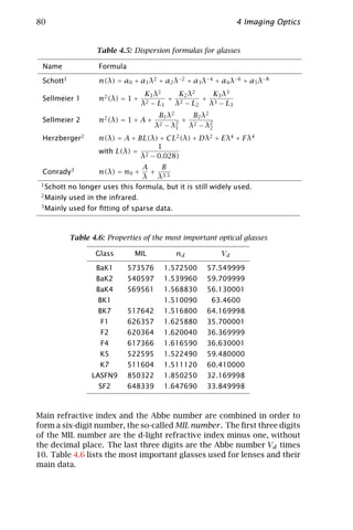
![4.5 Aberrations 81
Table 4.7: Optical properties of the most important plastics
Material MIL nd Vd
Polystyrol 1.590 30.8
Polycarbonat 1.585 30.0
PMMA (Perspex) 1.491 57.2
CR 39 1.499 57.8
a
n b
1. 35
1. 345
1. 34
1. 335
0. 4 0. 5 0. 6 0. 7 0. 8
Wavelength [ µm]
Figure 4.14: a Refractive index n of fresh water; b absorption coefficients of
fresh water, salt water and sea water.
In addition to optical glasses, some plastics are used for optical com-
ponents as well. Mainly Polystyrol and Perspex (Polymethylmethacrylic,
PMMA) are used. Because of the limited variety of refractive indices and
Abbe numbers, plastics are less flexible than glasses in optical design.
However, they are very suitable for the inexpensive production of as-
pherical and free-from elements by injection molding. Moreover, they
may be preferable because of their light weight.
4.4.3 Other materials
Similar to the glasses, fluids are characterized mainly by their refractive
index, Abbe number and absorption coefficient. Figure 4.14 shows the
refractive index n(λ) and the absorption coefficient of water.
4.5 Aberrations
So far, lenses have been described by the paraxial approximation. With-
in the limits of this approximation, perfect image quality is achieved. In
practice, an optics never reaches this ideal behavior, but shows degra-
dations of image quality caused by aberrations of the optics. These are
divided into two main classes according to their cause. The change of](https://image.slidesharecdn.com/computervision-handbookofcomputervisionandapplicationsvolume1-sensorsandimaging-120205081125-phpapp02/85/Computer-vision-handbook-of-computer-vision-and-applications-volume-1-sensors-and-imaging-106-320.jpg)
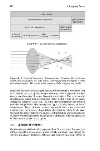

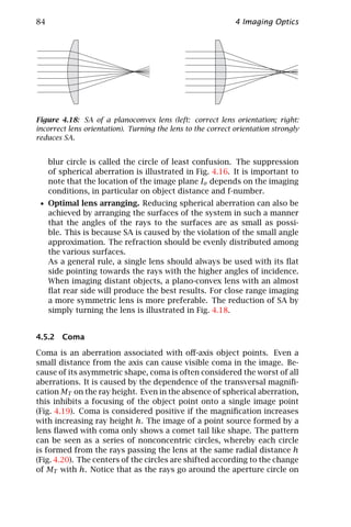


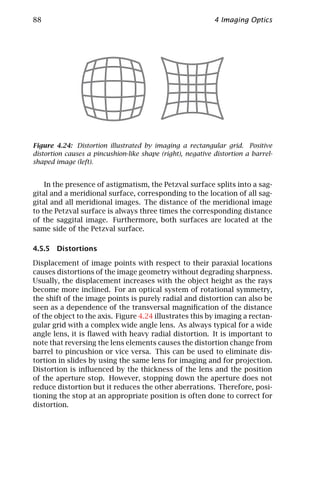


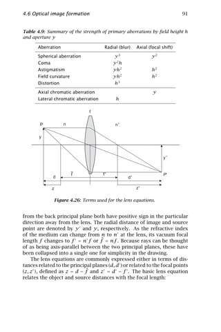
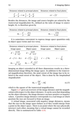


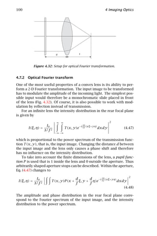
![4.8 References 101
4.8 References
[1] Schröder, G., (1990). Technische Optik, 7th edition. Würzburg: Vogel
Buchverlag.
[2] Hecht, E. and Zajac, A., (1977). Optics, 2nd edition. Addison Wesley World
Student Series. Reading, MA: Addison Wesley.
[3] Schott. Schott’96—Schott Optical Glass Catalog. Schott Glass Tech-
nologies Inc., 400 York Avenue Duryea, PA 18642 USA, (1996).
http://www.schottglasstech.com/SGTDnLoad.html.
[4] Shifrin, K. S., (1988). Physical Optics of Ocean Water. AIP Translation
Series. New York: American Institute of Physics.
[5] Sullivan, S. A., (1963). Experimental study of the absorption in distilled
water, artificial water and heavy water in the visible region of the spec-
trum. Jour. Optical Soc. America, 53:962–967.
[6] Driscoll, W. E. and Vaughan, W. (eds.), (1978). Handbook of Optics. New
York: McGraw-Hill Publishing Company.
[7] Tyler, J. E., (1978). Optical Properties of Water. In Handbook of Optics,
W. E. Driscoll, ed. New York: McGraw-Hill Publishing Company.
[8] Goodman, J. W., (1996). Introduction to Fourier Optics, 2nd edition. New
York: McGraw-Hill Publishing Company.
[9] Welford, W. T., (1991). Useful Optics. Chicago Lectures in Physics. Chicago
and London: The University of Chicago Press.
[10] Welford, W. T., (1991). Abberration of Optical Systems. The Adam Hilger
Series on Optics and Optoelectronics. Bristol: Adam Hilger.
[11] Smith, W. J., (1990). Modern Optical Design—The Design of Optical Sys-
tems. Optical and Electro-Optical Engineering Series. New York: McGraw
Hill.
[12] Yariv, A., (1991). Optical Electronics, 4th edition. Fort Worth: Saunders
College Publishing.
[13] Spinder & Hoyer, (1998). Gesamtkatalog G4. Göttingen: Spindler & Hoyer.
http://spindlerhoyer.de.
[14] Klein, V., Miles and Furtak, E., Thomas, (1996). Optics, 2nd edition. New
York: John Wiley & Sons (Sd). ISBN 0471872970.](https://image.slidesharecdn.com/computervision-handbookofcomputervisionandapplicationsvolume1-sensorsandimaging-120205081125-phpapp02/85/Computer-vision-handbook-of-computer-vision-and-applications-volume-1-sensors-and-imaging-126-320.jpg)


![106 5 Radiometry of Imaging
2. directly proportional to the areas of the emitting and receiving sur-
faces dS, and dR, respectively;
3. inversely proportional to the square of the distance r between emit-
ting and receiving surface (inverse square law); and
4. finally, it depends upon the orientation of the surface normals of dS
and dR with respect to the direction connecting the two surfaces.
The most important fact is that the received flux is directly propor-
tional to the radiance of the emitting surface. We will further show
that this proportionality remains for all further considerations lead-
ing towards the final imaging detector. Thus, the basic property to be
measured by radiometry is the radiance of the objects!
For finite size sources and detectors, we need to integrate Eq. (5.3)
over the surface areas S and R of source and detector, respectively,
cos θ cos θ
Φ= L dS dR (5.4)
S R r2
The average irradiance E of the receiving detector element is given by:
dΦ cos θ cos θ
E= = L dS (5.5)
dR S r2
The integrals Eq. (5.4) and Eq. (5.5) are the fundamental equations
describing the transfer of radiation from a source surface to a detector
surface [1]. These integrals, however, can only be solved analytically
for simple geometrical setups.
For practical applications it is common to separate the geometrical
aspects of the radiative transfer from the magnitude and spectral dis-
tribution of the radiance by defining a configuration factor . It is defined
as ratio of the flux Φr on the receiver by the total emitted flux of the
source, Φs [1]:
S R L cos θ cos θ r −2 dS dR
Fs −r = (5.6)
S 2π L cos θ dS dΩ
where the integration of the denominator of Eq. (5.6) is carried out
over the entire hemispheric enclosure. The indices Fs −r indicate the
flux transfer from source to receiver. In case of a Lambertian source,
the radiance can be drawn out of the integrals and Eq. (5.6) reduces to
1
Fs −r = cos θ cos θ r −2 dS dR (5.7)
πS S R
which contains only geometrical quantities. For homogeneous Lamber-
tian sources with radiance Ls , the exchanged flux is given by
Φs −r = π Ls SFs −r (5.8)](https://image.slidesharecdn.com/computervision-handbookofcomputervisionandapplicationsvolume1-sensorsandimaging-120205081125-phpapp02/85/Computer-vision-handbook-of-computer-vision-and-applications-volume-1-sensors-and-imaging-131-320.jpg)
![5.2 Observing surfaces 107
S/cosθ
dS
S A R
r
θ l
Figure 5.2: Schematic setup of radiance meter (Gershun tube).
Thus, if the geometry of the setup remains unchanged, the configura-
tion factor stays constant and we can focus on the variable portions of
the detector flux or irradiance.
More details on configuration factors are given by [2] and [1]. Tab-
ulated values and approximated equations for a variety of geometrical
setups can be found in [3].
If we just place a detector into a scene, all surface areas within the
3-D enclosure contribute to detector irradiance. Thus, we have to in-
tegrate Eq. (5.5) over the entire surface of all surrounding—arbitrarily
shaped—objects. Apart from the mathematical difficulties, this inte-
gration yields the average irradiance of the detector surface element,
rather than an “image” of the individual object surfaces. In order to
resolve spatial variations of emitting surfaces, we need to restrict the
allowed angles of incidence.
Section 5.2.2 outlines the principal setup of a point measuring ra-
diometer and the basic radiometric properties, which constitute the
basis for imaging systems.
5.2.2 Radiance meter
A simple radiance meter can be set up by a radiation detector R placed
at the bottom of a tube of length l, with a welldefined aperture of diam-
eter A on top. Such a device is commonly referred to as Gershun tube
in the literature. Figure 5.2 illustrates the principal geometric relation-
ships.
The entrance aperture of the radiometer limits incident radiation to
a conical solid angle
S A
Ωs = = 2 (5.9)
r2 l](https://image.slidesharecdn.com/computervision-handbookofcomputervisionandapplicationsvolume1-sensorsandimaging-120205081125-phpapp02/85/Computer-vision-handbook-of-computer-vision-and-applications-volume-1-sensors-and-imaging-132-320.jpg)


![110 5 Radiometry of Imaging
b
240 reflection coating
a white paper
glossy cardboard
brightness [gray values]
200 brushed aluminum
CCD
matte blue paper
160
120
θi θ 80
40
0
0 10 20 30 40 50 60 70 80 90
angle [°]
Figure 5.3: Lambertian surface observed under different angles with fixed illu-
mination: a experimental setup; b apparent surface brightness vs observation
angle for different surfaces.
source is considered to be far away from the surface, producing a con-
stant irradiance E(x) = E over S. A camera is observing the surface
under changing observation angles, 0 ≤ θ < 90° (Fig. 5.3a).
If the surface is Lambertian and the illumination source is fixed, the
measured image brightness should remain constant with respect to θ
(Eq. (5.14)).
For non-Lambertian surfaces, the brightness should exhibit a faster
decrease with respect to the angle θ. Figure 5.3b shows the angu-
lar dependence of the apparent brightness for several different sur-
faces. The surface brightness is averaged over a fixed area of interest
within the image for angular steps of 1°. The solid line corresponds
to a commercial matte reflection coating with a high reflectivity of
˜
ρ = 0.99. It has the highest apparent brightness in the images. How-
ever, it does not show an angle-independent brightness. White paper
shows a similar angular dependence but has a lower reflectivity. The
fastest decrease in brightness with respect to angle can be observed
for the glossy cardboard, which exhibits a mixture of specular and
matte reflection.
A remarkable example for Lambertian surface characteristics can be
observed with matte blue paper. Although having the lowest bright-
ness, the angular dependence remains almost constant for angles up
to 85°.
Brushed aluminum shows almost the same quasi-Lambertian behavior
except that the specular component of the surface reflectivity leads
to intermittent brightness changes with respect to the observation
angle. It is important to note that all surfaces show a fast brightness
decrease towards zero for angles close to 90°. The measurement, how-
ever, could not be carried out for angles above 88°.](https://image.slidesharecdn.com/computervision-handbookofcomputervisionandapplicationsvolume1-sensorsandimaging-120205081125-phpapp02/85/Computer-vision-handbook-of-computer-vision-and-applications-volume-1-sensors-and-imaging-135-320.jpg)
![5.2 Observing surfaces 111
b
240
a reflection coating
white paper
brightness [gray values]
200 glossy cardboard
CCD
brushed aluminum
matte blue paper
160
120
θ 80
40
0
0 10 20 30 40 50 60 70 80 90
angle [°]
Figure 5.4: Surface under different combined illumination/observation angles:
a experimental setup; b apparent surface brightness vs observation angle for
different surfaces.
Example 5.2: Illumination under different angles
Instead of a fixed illumination, we attach the light source to the cam-
era, which is again observing a surface under changing observation
angles (Fig. 5.4).
Now, the irradiance of the surface S is changing with the angle of
incidence, according to
E(θ) = E(0) cos θ (5.15)
as the same amount of radiative flux is spread over a larger area with
increasing angle. Hence, even a Lambertian surface shows a cosine
dependence of the image brightness with increasing angle. This is the
case because the reflected radiance remains constant for changing
viewing angles of Lambertian surfaces. The reflection, however, is
proportional to the irradiance of the surface.
A non-Lambertian surface shows a much faster decrease with angle, as
the decreasing irradiance and the angular decrease of the reflectivity
add up. Figure 5.4b shows the angular dependence of the apparent
brightness for the same surfaces as already shown in Example 5.1.
Although they differ by the absolute brightness due to the different
surface reflectivities, they all are dominated by the cosine relationship.
Non-Lambertian surfaces, however, show a faster decrease at large an-
gles than that of Lambertian surfaces (compare Fig. 5.3b and Fig. 5.4b).
Again, the brushed aluminum exhibits a strong variation of the sur-
face brightness due to specular reflection.](https://image.slidesharecdn.com/computervision-handbookofcomputervisionandapplicationsvolume1-sensorsandimaging-120205081125-phpapp02/85/Computer-vision-handbook-of-computer-vision-and-applications-volume-1-sensors-and-imaging-136-320.jpg)
![112 5 Radiometry of Imaging
b
180
a 160
brightness [gray values]
140
120
100
C
D
C 80
60
θ 40
20
0
0 1 2 3 4 5 6 7
-2
inverse squared distance [m ]
Figure 5.5: Inverse-square law of irradiation on a surface: a experimental
setup; b measured brightness vs distance, together with fitted inverse-square
relationship.
Example 5.3: Inverse-square law
In order to verify the inverse-square law, which has been derived in
Chapter 2 (Eq. (2.26)), we need to move a point light source along
a straight line perpendicular to the surface under observation. The
experimental setup consists of a long (4 m) optical bench. The cam-
era is fixed with respect to the surface, under an observation angle
of θ = 45°, such that it does not block light from the light source
(Fig. 5.5a).
Figure 5.5b shows the resulting image brightness with respect to the
distance d between light source and surface. The image of the surface
was averaged over a fixed area of interest and plotted vs the inverse
squared distance, d−2 . In this way, the inverse-square law reduces to
a linear relationship. A linear fit of the measured data shows that the
inverse-square law can be experimentally verified.
5.3 Propagating radiance
In Section 5.2 we learned that a radiometer serves as a radiance meter ,
which produces an output proportional to the radiance of the observed
surfaces. Before we turn towards the question of how the radiance dis-
tribution of an object surface is converted into irradiance of the sensor
plane by the optical image formation process, we need to consider ex-
actly what happens to radiance when propagating through space and
passing the camera lens system. We will derive a fundamental law of
radiometry—referred to as radiance invariance—which constitutes the
basis for all radiometric measurements. The derivation of this law fol-
lows McCluney [1] and Nicodemus [4].](https://image.slidesharecdn.com/computervision-handbookofcomputervisionandapplicationsvolume1-sensorsandimaging-120205081125-phpapp02/85/Computer-vision-handbook-of-computer-vision-and-applications-volume-1-sensors-and-imaging-137-320.jpg)


![118 5 Radiometry of Imaging
Another factor further reducing the irradiance E (P ) is given by
the fact that the solid angle Ω, subtended by the lens, decreases pro-
portional to cos θP (Eq. (2.5), see Chapter 2). Thus, the effective lens
aperture is reduced by the projection onto the viewing direction.
Finally, the irradiance E (P ) at the detector plane is proportional to
the angle of incidence, which is also given by cos θP .
Combining all influences decreasing the irradiance E , we get the
following result for off-axis points:
E (P ) = E (Po ) cos4 θP (5.33)
This cos4 -dependence is known as field darkening, reducing the irradi-
ance towards the edge of the sensor plane.
Typical values of the relative decrease of irradiance at the edge of
the image compared to the center point are in the order of 10 % and
0.5 % for f = 25 mm and 100 mm, respectively. With increasing focal
length, the field darkening is expressed less. For wide-angle lenses,
however, this effect can not be neglected. Volume 3, Fig. 32.3b shows
an example of an image taken with a wide-angle endoscope optic. The
field darkening is clearly visible.
Vignetting. In addition to the cos4 -dependence of the irradiance across
the sensor plane, other optical effects contribute to the resulting field
darkening of an image. The term vignetting is used for effects block-
ing off-axis rays by internal aperture stops of the lens system or other
beam-delimiting components [1]. Such effects produce an additional
decline of the image irradiance towards the edge of the image.
5.5 Detecting radiance
The final step in the chain of radiometric imaging is the detection of ra-
diation at the imaging sensor. Here, the irradiance of the sensor plane
is converted into an electronic signal. Without going into details of
solid state physics, this section outlines the basic properties of imag-
ing detectors relevant for a quantitative radiometric interpretation of
images. More detailed overviews of detectors for electromagnetic radi-
ation can be found in the following excellent textbooks [1, 5, 6], as well
as in standard handbooks on radiometry, such as [3].
5.5.1 Detector performance: figures of merit
Before we turn towards a classification of optical detectors in terms of
their operational principle, we will summarize commonly used figures
of merit, which allow us to compare the relative performance between](https://image.slidesharecdn.com/computervision-handbookofcomputervisionandapplicationsvolume1-sensorsandimaging-120205081125-phpapp02/85/Computer-vision-handbook-of-computer-vision-and-applications-volume-1-sensors-and-imaging-143-320.jpg)
![5.5 Detecting radiance 119
a b
η R
λc λ λc λ
Figure 5.9: Response of an ideal photodetector. a Quantum efficiency; and b
responsivity. Solid lines correspond to ideal detectors and dashed lines to typical
departures from ideal curves (After [5]).
detectors. These quantities also constitute the link between the radio-
metric quantities of radiation impinging on the detector material and
the final electrical detector output.
Quantum efficiency. Quantum efficiency η(λ) relates the number of
photons incident on the detector to the number of independent elec-
trons generated. It counts only primary charge carriers directly related
to the initial absorption process and does not count electrical amplifi-
cation. Quantum efficiency takes into account all processes related to
photon losses, such as absorptance of the detector material, scattering,
reflectance and electron recombination.
In a more general sense, the CIE vocabulary defines quantum effi-
ciency as the ratio of elementary events contributing to the detector
output to the number of incident photons. This also accounts for de-
tectors in which no charge carriers are directly released by photon ab-
sorption. The quantum efficiency can be expressed as
no
η(λ) = (5.34)
np
where np is the number of incident photons; no defines the number
of output events, such as photoelectrons in photodiodes, and electron-
hole pairs in semiconductors (Section 5.5.2).
The quantum efficiency is always smaller than one and is commonly
expressed in per cent. Figure 5.9a shows the spectral quantum effi-
ciency for an ideal photodetector. The ideal quantum efficiency is a
binary function of wavelength. Above a certain cutoff wavelength λc ,
photons have insufficient energy to produce photogenerated charge
carriers (Section 5.5.2). All photons with higher energy (smaller wave-
lengths) should produce the same output. Real photodetectors show
a slightly different behavior. Near λc the thermal excitation of the de-
tector material can affect the production of charge carriers by photon](https://image.slidesharecdn.com/computervision-handbookofcomputervisionandapplicationsvolume1-sensorsandimaging-120205081125-phpapp02/85/Computer-vision-handbook-of-computer-vision-and-applications-volume-1-sensors-and-imaging-144-320.jpg)


![5.5 Detecting radiance 123
a b c
- conduction band conduction band - conduction band
Qi
+
hν
Qg Qg Qg
-
hν
hν
Qi
+ valence band + valence band valence band
intrinsic (pure) acceptor, p-type impurity donor, n-type impurity
Figure 5.10: Energy-band diagrams for a intrinsic photoconductors; b extrinsic
p-type photoconductors; and c extrinsic n-type photoconductors.
Table 5.1: Intrinsic photoconductor materials. 1 Values taken from [6]. 2 Values
computed by the author.
Material η (%) λc (µm) T (K)
GaAs2 - 0.9 300
Si2 - 1.1 300
Ge2 - 1.9 300
PbS1 50 3 300
PbSe1 50 5 300
InSb2 - 6.9 77
HgCdTe1 60 25 77
tographic films, most photon detectors are solid state detectors, which
make use of the fact that electrical properties of semiconductors are
dramatically altered by the absorption of ultraviolet, visible and in-
frared photons.
Intrinsic photoconductors. Photoconductors respond to light by ei-
ther changing resistance or conductance of the detector material. In-
trinsic photoconductors are the most straightforward way to design a
solid state electronic detector. They make use of the inherent electrical
property of pure semiconductor materials without additional manipu-
lations. At normal temperatures, relatively few electrons will be in the
conduction band of a semiconductor, which results in a low electric
conductivity of the material. Figure 5.10a illustrates the energy-band
diagram for an intrinsic photoconductor.
In order to move from the valence band into the conduction band,
an electron must have sufficient energy. By absorbing a photon whose
energy is greater than that of the bandgap energy Qg , an electronic
bond can be broken and the electron can be lifted into the conduction](https://image.slidesharecdn.com/computervision-handbookofcomputervisionandapplicationsvolume1-sensorsandimaging-120205081125-phpapp02/85/Computer-vision-handbook-of-computer-vision-and-applications-volume-1-sensors-and-imaging-148-320.jpg)
![124 5 Radiometry of Imaging
band, creating an electron/hole pair (Fig. 5.10a). Both the electron and
the corresponding hole can migrate through the detector material and
contribute to the conductivity. If an electric field is maintained across
the detector, any absorbed photon results in a small electric current,
which can be measured by a high-impedance amplifier.
As thermal excitation contributes to the conductivity in the same
way as absorbed radiation, thermal noise will corrupt the signal, espe-
cially at high temperatures and low illumination levels. The number of
thermally exited electrons follows the Boltzmann distribution:
Qg
nt ∝ exp − (5.42)
kB T
where Qg , kB , and T are the bandgap energy, the Boltzmann constant,
and the absolute temperature, respectively. As Qg becomes smaller,
the number of thermally exited charge carriers increases. One way
to overcome this problem is to cool the detector down to cryogenic
temperatures below 77 K (liquid nitrogen temperature), where thermal
excitation is negligible.
The minimum photon energy that can be detected is given be the
bandgap energy Qg of the detector material. With the photon energy
(Eq. (2.2))
hc
ep = hν = (5.43)
λ
the maximum detectable wavelength λc , commonly referred to as cutoff
wavelength, is given by
hc
λc = (5.44)
Qg
Substituting for the constants, and correcting for units such that wave-
lengths are in microns and energy gap in electron volts yields the fol-
lowing rule of thumb:
1.238
λc [µm] = (5.45)
Qg [eV]
Table 5.1 shows some examples of common materials used to manu-
facture intrinsic photoconductive detectors, together with the quantum
efficiency, the cutoff wavelength, and the operating temperature.
Intrinsic photoconductor detectors can be made in large arrays and
they have good uniformity and high quantum efficiency, typically in the
order of 60 %. They are the basic components of CCD-arrays (charge
coupled devices), which are the most widely used 2-D detectors in the
visible, the near infrared, and—to some extent—in the x-ray and ultravi-
olet region using special semiconductor compounds. In the infrared re-
gion, semiconductors with a small bandgap have to be used. For highly](https://image.slidesharecdn.com/computervision-handbookofcomputervisionandapplicationsvolume1-sensorsandimaging-120205081125-phpapp02/85/Computer-vision-handbook-of-computer-vision-and-applications-volume-1-sensors-and-imaging-149-320.jpg)
![5.5 Detecting radiance 125
Table 5.2: Extrinsic photoconductor materials. 1 Values taken from [6]. 2 Values
taken from [5].
Material η (%) λc (µm) T (K) Material η (%) λc (µm) T (K)
Ge:Hg1 30 14 4 Si:Cu2 - 5.2 -
Ge:Cu1 30 27 4 Si:In1 40 8 45
Ge:Be2 - 52 - Si:Be2 - 8.3 -
Ge:As2 - 98 - Si:Al2 - 18.5 -
Ge:P2 - 103 - Si:Ga1 40 19 18
Ge:Ga2 - 115 - Si:As1 40 24 4
Ge:B2 - 119 - Si:B2 - 28 -
Ge:In1 30 120 4 Si:P1 40 29 12
Ge:Sb2 - 129 - Si:Sb2 - 29 -
energetic radiation, such as x-rays, the energy exceeds the bandgap of
any semiconductor. However, the absorption coefficient of most mate-
rials is extremely low at these wavelengths, which makes most sensors
almost transparent to short-wave radiation. In order to deposit the en-
ergy in the detector, the semiconductor material must contain heavy
atoms, which have a higher absorptivity in the x-ray region.
Extrinsic photoconductors. For longer wavelengths toward the in-
frared region, it is hard to find suitable intrinsic semiconductor mate-
rials with sufficiently small bandgaps. For wavelengths beyond 15 µm,
materials tend to become unstable and difficulties occur in achieving
high uniformity and making good electrical contacts. A solution to this
problem is to use extrinsic photoconductors, that is, semiconductors
doped with either p-type or n-type impurities.
The addition of impurities places available electron states in the pre-
viously forbidden gap and allows conductivity to be induced by freeing
impurity-based charge carriers. Thus, smaller energy increments are
required. As illustrated in Fig. 5.10b and c, only the gap between the
valence band and the impurity level (p-type semiconductors) or the gap
between the impurity level and the conduction band (n-type semicon-
ductors) has to be overcome by absorption of a photon. In the former
case, the conductivity is carried by holes and in the latter case free
electrons in the conduction band contribute to the conductivity. The
basic operation of extrinsic photoconductors is similar to that of in-
trinsic photoconductors, except that the bandgap energy Qg has to be
replaced by the excitation energy Qi (Fig. 5.10b and c).
Table 5.2 shows some examples of common materials used to man-
ufacture extrinsic photoconductive detectors, together with the quan-](https://image.slidesharecdn.com/computervision-handbookofcomputervisionandapplicationsvolume1-sensorsandimaging-120205081125-phpapp02/85/Computer-vision-handbook-of-computer-vision-and-applications-volume-1-sensors-and-imaging-150-320.jpg)

![5.5 Detecting radiance 127
Table 5.3: Photovoltaic (photodiode) detector materials. Values taken from [6].
Material η (%) λc (µm) T (K)
GaAsP 60 0.7 300
Si 65 1.1 300
InGaAs 86 1.7 300
Ge 64 1.8 300
InAs 40 3.3 77
HgCdTe 65 5 77
InSb 45 5.5 77
Photodiodes (photovoltaic detectors). A photovoltaic detector ac-
tively generates a voltage or current from incident electromagnetic ra-
diation. The most common realization is based on a junction between
two oppositely doped zones (p-n junction) in a semiconductor mate-
rial. As this setup acts as a diode, this type of detector is also called
photodiode.
Photodiodes allow large resistance and simultaneously high pho-
toconductive gain within a small volume to be obtained. The n-type
material has a surplus (and the p-type material has a deficiency) of elec-
trons compared to the crystal bond of the semiconductor material. In
the adjacent region of both oppositely doped zones, electrons migrate
from the n- to the p-region acceptor atoms and holes migrate from
the p- to the n-region donors, if thermal excitation frees them. Within
the contact region all bonds are complete and the material is depleted
of potential charge carriers. This results in a high resistance of this re-
gion, as opposed to the relatively high conductivity of the p- and n-type
material. As the charge carriers diffuse, a voltage is established across
the depletion region, called the contact potential, which opposes the
diffusion of additional electrons. The net result is a permanent equi-
librium voltage across the p-n junction. The resulting bandstructure
across the contact zone is shown in Fig. 5.11.
Table 5.3 shows some examples of common materials used to man-
ufacture photodiode detectors, together with the quantum efficiency,
the cutoff wavelength, and the operating temperature.
When photons of energies greater than the forbidden gap energy are
absorbed in, or close to a p-n junction of a photodiode, the resulting
electron/hole pairs are pulled by the electric field of the contact po-
tential across the p-n junction. Electrons are swept from the p-region
into the n-region, and holes in the opposite direction (Fig. 5.11). As the
charge carriers are spatially separated across the detector, a resulting](https://image.slidesharecdn.com/computervision-handbookofcomputervisionandapplicationsvolume1-sensorsandimaging-120205081125-phpapp02/85/Computer-vision-handbook-of-computer-vision-and-applications-volume-1-sensors-and-imaging-152-320.jpg)
![128 5 Radiometry of Imaging
b
a
anode
vacuum -
hν
microchannel
-
photocathode
photo-
electron
Vout
Vsupp
-
photomultiplier tube
Figure 5.12: Photoemissive detectors. a Detection process for a vacuum photo-
diode; b light amplification by a microchannel (top) and a photomultiplier tube
(bottom).
voltage can be measured. If the n- and the p-type region are connected,
a small current will flow between both regions. This phenomenon is
called the photovoltaic effect .
Because photodiodes operate through intrinsic rather than extrin-
sic absorption, they can achieve a high quantum efficiency in small vol-
umes (Table 5.3). Photodiodes can be constructed in large arrays of
many thousands of pixels. They are the most commonly used detec-
tors in 1-6-µm region [5] (e. g., InSb infrared focal plane arrays) and are
also used in the visible and near ultraviolet.
Photoemissive detectors. Photoemissive detectors operate with exter-
nal photoelectric emission. The excited electron physically leaves the
detector material and moves to the detecting anode. Figure 5.12a il-
lustrates the principal setup. A conduction electron is produced in the
photocathode by absorption of a photon with an energy greater than
the intrinsic bandgap of the detector material. This electron diffuses
through the detector material until it reaches the surface. At the sur-
face of the photocathode it might escape into the vacuum. Using an
electric field between the photocathode and the anode helps to acceler-
ate the electron into the vacuum, where it is driven towards the anode
and counted as current.
Suitable photocathode materials must have the following proper-
ties:
• high-absorption coefficient for photons
• long mean-free path for the electron in the cathode material (low
transport losses of electrons migrating to the surface of the cathode)](https://image.slidesharecdn.com/computervision-handbookofcomputervisionandapplicationsvolume1-sensorsandimaging-120205081125-phpapp02/85/Computer-vision-handbook-of-computer-vision-and-applications-volume-1-sensors-and-imaging-153-320.jpg)
![5.5 Detecting radiance 129
Table 5.4: Photocathode materials. Values taken from [6].
Material η (%) λc
(µm)
GaAsP (NEA) 30 0.9
Cs-Nag-K-Sb (S20) 20 0.9
Ag-O-Cs (S1) 1 1.1
• low electron affinity, that is, low barrier inhibiting the electron emis-
sion
Table 5.4 summarizes common materials used for the fabrication of
photocathodes in photoemissive detectors.
The simple vacuum photodiode, illustrated in Fig. 5.12a, can be
improved by electron multipliers, increasing the number of electrons
contributing to the output current for each detected photon. A com-
monly used photoemissive detector is the photomultiplier , illustrated
in Fig. 5.12b. It consists of a vacuum tube including several interme-
diate anodes. Each anode, called a dynode, is given a voltage higher
than the previous one. The geometrical arrangement is such that emit-
ted electrons are accelerated towards the next adjacent dynode. If the
voltage difference is high enough, each photoelectron leaving a dynode
gets fast enough to eject multiple electrons from the next dynode upon
impact. This process is repeated until the avalanche of electrons finally
reaches the anode. The voltages required for operation are provided
by a single supply, divided by a chain of resistors. The photocathode is
held at a large negative voltage in the order of several thousand volts
relative to the anode.
Photomultipliers are large devices, restricted mainly to single de-
tectors. A different form of electron multipliers, which is of practical
relevance for computer vision, are made from thin tubes of lead-oxide
glass. These microchannels have diameters of 8-45 µm and a length-
to-diameter ratio of about 40 [5], and are suitable for integration into
small-scale detector arrays. Microchannel plates are arrays of approx-
imately one million channel electron multipliers, fused into solid wa-
vers [7]. Figure 5.12b illustrates the principal mechanism of a single
microchannel. The microchannel wall consists of three layers: an emit-
ting layer; a conducting layer; and bulk glass. The conductive layer has
a high resistance and allows a large voltage to be maintained across the
ends of the tube. Electrons that enter the tube are accelerated along
the tube until they collide with the wall. The inner surface layer, called
the emitting layer, is made from PbO, which acts as an electron multi-
plier. Upon impact, the accelerated electrons create multiple secondary
electrons that are accelerated by the voltage along the tube until they](https://image.slidesharecdn.com/computervision-handbookofcomputervisionandapplicationsvolume1-sensorsandimaging-120205081125-phpapp02/85/Computer-vision-handbook-of-computer-vision-and-applications-volume-1-sensors-and-imaging-154-320.jpg)
![130 5 Radiometry of Imaging
strike the walls again and produce more free electrons. This operation
is comparable to a continuous dynode chain and the gains are nearly
as large as those of photomultipliers.
Microchannel plates are used in modern light intensifying cameras,
suitable for low-illumination applications, such as fluorescence imaging
and night vision devices.
5.5.4 Thermal detectors
The first detectors discovered were thermal detectors, which showed
a response to the heating effect of radiation. Unlike photon detectors,
they do not respond to charge carriers, directly excited by absorbed
photons. Instead, the thermal energy of absorbed photons is detected
by temperature-dependent physical processes. A thermal detector can
be thought of as two essential parts: the absorber and the temperature
sensor.
It is important to note that the net energy stored by absorption is
given by the photon energy times the number of absorbed photons.
Thus, low-energy photons can create the same detector output as high-
energy photons, if the photon flux is higher and compensates for the
lower energy. For this reason, the spectral response of thermal detec-
tors is flat and determined by the spectral dependence of the surface
absorptance.
Thermal detectors are either bulk devices or metal junction devices.
The junction devices, such as the thermocouple and thermopile, rely
upon the Seebeck effect or thermoelectric effect . Two separate junc-
tions of two dissimilar metals generate a voltage proportional to the
difference in temperature between them [1]. If one junction is kept
at reference temperature, the series output will be proportional to the
temperature of the other junction. In practical realizations of thermo-
couples, one junction is embedded into an absorbing material, while
the other junction is thermally connected to the radiometer housing
with a high thermal mass. Thermopiles are series of individual thermo-
couples, which substantially increases the sensitivity.
While thermopiles are mostly used as single detectors, another type
of thermal detector, called a bolometer , is a bulk-type detector and can
be easily integrated into large detector arrays. Bolometers take advan-
tage of the high-temperature coefficient of resistance in semiconduc-
tors, which is similar to the principle of photoconductors. A detailed
treatment of recent developments in the fabrication of microbolometer
arrays is given in Chapter 10.
Recent developments in high-temperature (about 77 K) supercon-
ductivity made another type of thermal detectors available, which relies
on the sharp resistance change with temperature in the superconduct-
ing transition region. These superconducting bolometers can also be](https://image.slidesharecdn.com/computervision-handbookofcomputervisionandapplicationsvolume1-sensorsandimaging-120205081125-phpapp02/85/Computer-vision-handbook-of-computer-vision-and-applications-volume-1-sensors-and-imaging-155-320.jpg)
![5.5 Detecting radiance 131
1.5
1
0.5
0
-0.5
-1
-1.5
40 50 60 70 80
Figure 5.13: Mixing of two periodic signals Si , and Sm with slightly different
wavelengths, λi = 1.1 λm . The bold line shows the resulting signal S = Si + Sm .
The amplitude of the mixed signal is modulated by the difference, or beat, fre-
quency.
operated in two other modes that involve the breaking of Cooper pairs
by the incident photons, thus destroying superconductivity [6].
Coherent detectors. Coherent receivers directly measure the electro-
magnetic field of the incident radiation. They mix the electromagnetic
field of the incoming photons with an internal reference field of simi-
lar frequency, produced by a high-frequency oscillator. The resulting
signal shows a strong modulation of the amplitude, which is given by
the difference frequency of both signals—a physical effect commonly
referred to as beating.
Let Si and Sm be the incident, and the mixing signal (electric field),
respectively, given in complex notation by
Sm = Am exp[iωt], and Si = Ai exp[i(ω + )t] (5.46)
where is a small frequency shift compared to the main frequency ω.
Linear superposition yields the following mixed signal:
S = Sm + Si = Am exp[iωt] + Ai exp[i(ω + )t]
(5.47)
= exp[iωt] (Am + Ai exp[i t])
which can be interpreted as an oscillation at the frequency ω, with an
amplitude modulation at the difference (beat) frequency . This effect
is illustrated in Fig. 5.13.
From the mixed field, the exact frequency can be extracted, as well
as the amplitude and phase of the incident signal. In order to measure
the electric field, the mixed field has to be passed through a nonlinear
electrical element, called mixer , that converts power from the original
frequency to the beat frequency.](https://image.slidesharecdn.com/computervision-handbookofcomputervisionandapplicationsvolume1-sensorsandimaging-120205081125-phpapp02/85/Computer-vision-handbook-of-computer-vision-and-applications-volume-1-sensors-and-imaging-156-320.jpg)
![132 5 Radiometry of Imaging
a b
incident flux
dp
ds photosensitive
photosensitive
Figure 5.14: Schematic illustration of the fill factor and microlens arrays on
detector arrays. a Detector without a microlens array; b Detector with a micro-
lens array.
Unlike all other types of (incoherent) receivers, these coherent re-
ceivers obtain additional information about the wave number and phase
of the signal. As the phase information is given, they can correlate mea-
surements of different receivers to reconstruct the incoming wavefront
by interferometry. Intercontinental baseline radio telescopes use this
ability to combine several telescopes spread over the entire globe to
enhance the resolution up to milliarc-seconds for astronomical appli-
cations.
A more detailed treatment of the theory of coherent receivers can
be found in [8] and [5].
5.5.5 Characteristics of detector arrays
Fill factor. Most detector arrays used in computer vision are not pho-
tosensitive over the entire detector area. As all electrical contacts and
microelectronic components have to be integrated into the chip sur-
face, only a small portion is retained for the actual photosensitive de-
tector area. Exceptions are 1-D detector arrays, where all electronic
components and bonds can be arranged alongside the detector, or back-
illuminated detector arrays.
The basic quantities defining the fill factor of the sensor are the pixel
pitch dp , which describes the center distance of two neighboring pixels,
and the pixel size ds , which is the extension of the photosensitive area.
For nonsquare pixels, the dimensions on both directions have to be
known.
Given a local irradiance Ei (x) on the sensor, only the portion
d2
s
E(x) = Ei (x) (5.48)
d2
p
actually contributes to the signal at the point x (Fig. 5.14a). For non-
square pixels/arrays, the squared quantities have to be replaced by the
products of the corresponding quantities in the x- and y-direction,
respectively.](https://image.slidesharecdn.com/computervision-handbookofcomputervisionandapplicationsvolume1-sensorsandimaging-120205081125-phpapp02/85/Computer-vision-handbook-of-computer-vision-and-applications-volume-1-sensors-and-imaging-157-320.jpg)

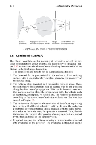
![5.7 References 135
detector plane shows a natural field darkening with decreasing irra-
diance towards the edges of the detector. This field darkening can
be further amplified by vignetting and other optical effects blocking
parts of the radiation.
5. The final output of the imaging detector depends on a variety of
detector properties. If the conversion from incident flux to an elec-
trical signal is linear, the output remains proportional to the object
irradiance.
5.7 References
[1] McCluney, W. R., (1994). Introduction to Radiometry and Photometry.
Boston: Artech House.
[2] Siegel, R. and Howell, J. R. (eds.), (1981). Thermal Radiation Heat Transfer,
2nd edition. New York: McGraw-Hill Book, Co.
[3] Wolfe, W. L. and Zissis, G. J. (eds.), (1989). The Infrared Handbook, 3rd
edition. Michigan: The Infrared Information Analysis (IRIA) Center, Envi-
ronmental Research Institute of Michigan.
[4] Nicodemus, F. E., (1963). Radiance. Am. J. Phys., 31:368–377.
[5] Rieke, G. H., (1994). Detection of Light: From the Ultraviolet to the Submil-
limeter. Cambridge: Cambridge University Press.
[6] Dereniak, E. L. and Boreman, G. D., (1996). Infrared Detectors and Systems.
New York: John Wiley & Sons, Inc.
[7] Laurin Publishing, (1998). The Photonics Design and Applications Hand-
book, 44th edition. Pittsfield, MA: Laurin Publishing CO.
[8] Torrey, H. C. and Whitmer, C. A., (1948). Crystal Rectifiers, Vol. 15. New
York: Massachusetts Institute of Technology Radiation Laboratory Series,
McGraw-Hill.](https://image.slidesharecdn.com/computervision-handbookofcomputervisionandapplicationsvolume1-sensorsandimaging-120205081125-phpapp02/85/Computer-vision-handbook-of-computer-vision-and-applications-volume-1-sensors-and-imaging-160-320.jpg)


![6.2 Natural illumination 139
2000
1800
spectral irradiance [Wm µm ]
-1
1600 0
1400
-2
1
1200
1000
2
800
600
4
400
200
0
0 0.5 1 1.5 2
wavelength [µm]
Figure 6.1: Solar irradiance: Comparison of the solar spectrum (solid lines) at
the top of the earth’s atmosphere to a blackbody at a temperature of 6000 K
(dashed line). Solar irradiance at sea level measured in multiples of the vertical
path through standard atmosphere, denoted as ma. The figure shows the ir-
radiance for ma = 0, 1, 2, and 4. With ma = 0, we denote the solar irradiance
right above the earth’s atmosphere, that is, without atmospheric absorption.
6.2.1 Solar radiation
Although solar radiation has the principal shape of blackbody radia-
tion (Fig. 6.1), the real origin is nuclear fusion rather than incandes-
cence. Powered from internal nuclear power, the outer regions of the
sun, heated up to a temperature of approximately 6000 K, emit thermal
radiation. On its way through the colder parts of the solar atmosphere
the radiation is subject to absorption (Section 3.4) from gases, which
shows up as narrow absorption lines, known as Fraunhofer lines. These
characteristic line spectra allow remote measurements of the presence
and concentration of extraterrestrial gases along the optical path.
Within the earth’s atmosphere additional absorption occurs. At sea
level parts of the solar emission spectrum are extinguished while oth-
ers remain almost unchanged (Fig. 6.1b). The latter parts are called
atmospheric windows and are of major importance for long distance
remote sensing. One example is the visible window, which is of major
importance for terrestrial life. Strong absorption regions visible in the
solar spectrum at sea level at about 0.9 µm, 1.1 µm, 1.4 µm, and 1.9 µm
(Fig. 6.1b), are caused by water vapor (H2 O) and carbon dioxide (CO2 ).
Another major attenuation line of CO2 is located in the IR part of
the spectrum at about 4.3 µm. This absorption line is of major impor-](https://image.slidesharecdn.com/computervision-handbookofcomputervisionandapplicationsvolume1-sensorsandimaging-120205081125-phpapp02/85/Computer-vision-handbook-of-computer-vision-and-applications-volume-1-sensors-and-imaging-164-320.jpg)
![140 6 Illumination Sources and Techniques
1.0
T = 30 mission
y
(clear ng
0 K sk
sky)
Esky(λ) (relative units)
ri
scatte
al e
therm
0.1
0.0
0.1 0.5 1 5 10 50
λ [µm]
Figure 6.2: Schematic illustration of the contributions from scattering and at-
mospheric emission to the diffuse background radiation.
tance for the greenhouse effect , responsible for global warming. The
increasing concentration of CO2 in the atmosphere causes an increas-
ing reabsorption of longwave IR radiation, which is emitted from the
earth’s surface, and thus increased heating up of the atmosphere.
The radiation luminous efficacy of solar irradiation can be deter-
mined to be approximately 90-120 lm W−1 for the lowest angle of inci-
dence (midday).
6.2.2 Diffuse sky irradiation
In addition to direct solar irradiation, natural illumination consists of
diffuse sky irradiation, commonly referred to as sky-background radia-
tion. It is caused by two major contributions: scattering of the sun’s ra-
diation for wavelengths shorter than 3 µm; and thermal emission from
the atmosphere for wavelengths beyond 4 µm (Fig. 6.2).
Depending on the cloud coverage of the sky, different scattering
mechanisms dominate. As already outlined in Section 3.4.1, the two
basic mechanisms are Rayleigh scatter , for particles smaller than the
wavelength, such as atmospheric molecules, and Mie scatter , for par-
ticles with sizes about the wavelength of the radiation, such as micro-
scopic water droplets. The solar scattering region dominates for wave-
lengths shorter than 3 µm because it is restricted to the region of solar
irradiance. The spectral distribution changes depending on the scat-
tering mechanism. For clear sky, Rayleigh scattering dominates, which
has a λ−4 wavelength dependence. Thus short wavelengths are more
efficiently scattered, which is the reason for the blue appearance of the
clear sky. For cloud-covered parts of the sky, Mie scatter dominates the
solar region. As this type of scattering shows a weaker wavelength de-
pendency (which is responsible for the greyish appearance of clouds),](https://image.slidesharecdn.com/computervision-handbookofcomputervisionandapplicationsvolume1-sensorsandimaging-120205081125-phpapp02/85/Computer-vision-handbook-of-computer-vision-and-applications-volume-1-sensors-and-imaging-165-320.jpg)

![142 6 Illumination Sources and Techniques
spectral irradiance [mWm-2nm-1]
10
6332
1 50W QTH
6282
50W Hg
6316
STD D2
0.1 6263 75W Xe
ozone free
6251 Std 75W Xe
200 400 600 800
wavelength [nm]
Figure 6.4: Overview of spectral irradiance curves for arc, quartz tungsten
halogen, and deuterium (D2 ) lamps at a distance of 0.5 m (Courtesy Oriel Cor-
poration, 1994).
optimized for specified applications. Figure 6.3 shows an overview of
available illumination sources for different spectral regions. In the fol-
lowing sections we will focus on the following illumination sources:
• incandescent lamps
• (arc) discharge lamps
• fluorescent lamps
• infrared emitters
• light emitting diodes (LED)
• laser
A more detailed overview can be found in [1], [2], and in catalogs of
manufacturers, such as the one from the Oriel Corporation [3].
6.3.1 Incandescent lamps
Incandescent lamps are among the most popular all-purpose illumina-
tion sources. The most prominent examples are standard light bulbs
used in almost every household. The classic light bulb uses a carbon
filament, which is placed in an evacuated glass enclosure in order to
avoid oxidation (burning) of the carbon filament.
More modern versions of incandescent lamps use tungsten filaments
instead of carbon fibers. The practical setup of tungsten incandescent
lamps are tungsten filaments of various shapes (rectangular dense and
coiled filaments) in quartz glass envelopes (Fig. 6.5). The coiled fil-
aments have an intensity distribution of circular symmetry about the](https://image.slidesharecdn.com/computervision-handbookofcomputervisionandapplicationsvolume1-sensorsandimaging-120205081125-phpapp02/85/Computer-vision-handbook-of-computer-vision-and-applications-volume-1-sensors-and-imaging-167-320.jpg)
![6.3 Artificial illumination sources 143
a
b
normal to
filament
filament
highest
irradiance
Figure 6.5: Quartz tungsten halogen incandescent lamps: a setup of a coiled
filament lamp; b setup of a rectangular filament lamp (Courtesy Oriel Corpo-
ration, 1994).
long axis of symmetry of the housing. For the rectangular filaments, the
light output strongly depends on the direction (Fig. 6.5b). The quartz
glass housing is transparent only for wavelengths up to 3 µm. It does,
however, heat up by absorption of long-wave radiation and thermally
emits infrared radiation corresponding to the glass temperature ex-
tending the spectrum into the mid-infrared region.
Incandescent lamps have a high visible and near infrared output.
˜
With an emissivity of tungsten of about ε = 0.4 (in the visible), the
spectral exitance of tungsten incandescent lamps is close to the exi-
tance of a graybody. It does, however, deviate for wavelengths of about
the peak wavelength and above. Figure 6.6 shows the spectral exitance
of an incandescent tungsten surface, compared to a graybody with an
˜
emissivity of ε = 0.425 at a color temperature of 3100 K.
The radiant efficiency of incandescent lamps is in the order of 80 %,
as incandescence very efficiently converts electrical input power into
radiant output. The output within the visible region, however, is much
lower. Operated at a color temperature of approximately 3000 K, tung-
sten incandescent lamps have a relatively low radiation luminous effi-
cacy of Kr = 21.2 lm W−1 , as the main part of the spectrum lies in the
infrared (Section 2.5.4). The lighting system luminous efficacy is only
Ks = 17.4 lm W−1 . The values are taken for an individual tungsten in-
candescent light bulb [4] and are subject to fluctuations for individual
realizations.
Two important modifications allow both radiant efficiency and the
lamp life to be increased:
1. In all tungsten filament lamps, the tungsten evaporates from the fil-
ament and is deposited on the inside of the envelope. This blackens](https://image.slidesharecdn.com/computervision-handbookofcomputervisionandapplicationsvolume1-sensorsandimaging-120205081125-phpapp02/85/Computer-vision-handbook-of-computer-vision-and-applications-volume-1-sensors-and-imaging-168-320.jpg)
![144 6 Illumination Sources and Techniques
3.5 × 10⁶
spectral exitance [Wm µm ]
1
-1
3.0 × 10⁶
-2
2.5 × 10⁶
2.0 × 10⁶
1.5 × 10⁶
2
1.0 × 10⁶
3
0.5 × 10⁶
0
0 0.5 1 1.5 2 2.5 3
wavelength [µm]
Figure 6.6: Spectral exitance of (1) a blackbody; (2) a graybody with emissivity
of = 0.425; and (3) a tungsten surface, all at a temperature of 3100 K (Courtesy
Oriel Corporation, 1994).
the bulb wall and thins the tungsten filament, gradually reducing
the light output. With tungsten halogen lamps, a halogen gas is
filled into the envelope. The halogen gas efficiently removes the de-
posited tungsten and returns it to the filament, leaving the inside of
the envelope clean, and providing long-term stability. This thermo-
chemical process is called the halogen cycle [3].
2. Some manufacturers produce new-generation halogen lamps with
infrared coatings on the envelope. These coatings are made such
that infrared radiation is reflected back onto the tungsten filament.
Thus, the temperature of the envelope and the infrared output of
the lamp are reduced, which increases luminous efficacy. At the
same time, the filament is heated by the emitted infrared radiation,
which yields a higher radiant efficiency, as less current is needed
to maintain the operating temperature. Both effects increase the
lighting system luminous efficacy.
As the exitance of an incandescent lamp is given by the tempera-
ture, which does not immediately follow changes in the voltage, the
light output does not follow rapid (kHz) voltage changes. It does, how-
ever, follow slow voltage changes, such as the net frequency under ac
operation, with an amplitude in the order of 10 % of the absolute exi-
tance [3]. This effect might cause beating effects, if the frame rate of
the video camera is at a similar frequency. For demanding radiomet-
ric applications it is recommended to use regulated dc power supplies.
The smaller the filament, the lower the thermal mass and the faster the
response of the lamp.](https://image.slidesharecdn.com/computervision-handbookofcomputervisionandapplicationsvolume1-sensorsandimaging-120205081125-phpapp02/85/Computer-vision-handbook-of-computer-vision-and-applications-volume-1-sensors-and-imaging-169-320.jpg)


![6.3 Artificial illumination sources 149
spectral irradiance [mWm nm ]
-1
-1 6575
10
6580
-2 -2
10
6363*
-3
10
6581
-4
10
-5
10
-6
10
1 3 5 7 9 11 13 15 17 19 21 23 25
wavelength [µm]
Figure 6.9: Spectral irradiance of IR sources (Courtesy Oriel Corporation,
1994).
6.3.4 Infrared emitters
Again, we return to thermal emission of radiation. As already dis-
cussed, quartz tungsten halogen lamps are excellent infrared sources,
emitting into the far infrared. They do, however, also emit a large por-
tion in the visible and near ultraviolet region. If this radiation is objec-
tionable, other sources of infrared radiation have to be used.
Common infrared sources are basically electrical resistance heaters.
The materials must have a high ohmic resistance to allow ohmic heat-
ing when an electric current is run through them. The surface must
be covered with a material that has a high emissivity in the infrared
region. Common materials are metals, ceramics, or carbon rods. Fig-
ure 6.9 shows several spectral outputs of commercially available in-
frared sources.
In the near infrared, a narrowband infrared emitter has become in-
creasingly important: these are the infrared LEDs, which are discussed
in Section 6.3.5.
6.3.5 Light-emitting diodes (LEDs)
This section is dedicated to light-emitting diodes (LEDs), small but nev-
ertheless powerful light sources, which have gained in importance dur-
ing the past few years. Originally intended as small signal lights for in-
strument panels, the performance of LEDs has dramatically increased,
while simultaneously the package size has decreased. Light-emitting
diodes are available in a huge variety of package sizes and spectral
ranges from blue light up to the near infrared.
The most important advantages of LEDs in terms of illumination
sources for computer vision can be summarized as follows:](https://image.slidesharecdn.com/computervision-handbookofcomputervisionandapplicationsvolume1-sensorsandimaging-120205081125-phpapp02/85/Computer-vision-handbook-of-computer-vision-and-applications-volume-1-sensors-and-imaging-174-320.jpg)
![150 6 Illumination Sources and Techniques
a b
1 1
0.8 0.8
0.6 0.6
0.4 0.4
0.2 λp λc 0.2
0
∆λ [nm]
0
400 450 500 550 600 λ [nm] 400 500 600 700 800 900 1000 λ [nm]
Figure 6.10: Spectral emissivity of LEDs: a typical relative spectral distribution
of an LED showing the location of the characteristic wavelengths and wave-
length intervals; b relative spectral distribution of the radiation emitted by a
series of typical LEDs and IREDs. Values have been normalized to unity at the
peak wavelength.
• high luminous efficacy
• small dimensions
• can be integrated into large arrays of arbitrarily any shape
• low power consumption, in the order of 20 m W
• fast response time, can be operated in pulsed mode
Basic operation. LEDs operate on the reversed physical process used
in photodiodes (see Section 5.5.2). They are made from a semiconduc-
tor material with a p-n junction operated in forward bias direction,
as opposed to the reverse bias operation of photodiode detectors (see
Fig. 5.11). If an external voltage is supplied in forward bias direction,
the sign of the applied potential is reversed, so it decreases the bias
across the depletion zone. If the bias voltage exceeds the contact volt-
age, the junction becomes strongly conducting. Charge carriers that
penetrate the p-n junction and enter the p- or n material can recombine
under emission of radiation. The wavelength of the emitted radiation
is given by the bandgap energy of the intrinsic semiconductor material.
Due to thermal excitation and impurities, the potential energy transi-
tions are not restricted to the bandgap energy but distributed about
this energy. Thus, emitted radiation is not fully monochromatic. It is,
however, limited to a narrow spectral range.
Spectral distributions. Figure 6.10a illustrates the typical shape of
the spectral distribution of an LED exitance Eλ . The characteristic wave-
lengths are the peak wavelength λp and the centroid wavelength λc](https://image.slidesharecdn.com/computervision-handbookofcomputervisionandapplicationsvolume1-sensorsandimaging-120205081125-phpapp02/85/Computer-vision-handbook-of-computer-vision-and-applications-volume-1-sensors-and-imaging-175-320.jpg)
![6.3 Artificial illumination sources 151
3 1 2
4
5
6
7
Figure 6.11: Examples of various package shapes and LED types. (1) Super-
bright SMD miniature LED HSMC-H670 (Hewlett Packard); (2) Superbright SMD
LED HLMP-Q105 (Hewlett Packard); (3) Miniature LED L10600ID (Kingbright);
(4) 2-mm package LED (noname); (5) 3-mm package LED HLMA-CH00 (Hewlett
Packard); (6) 5-mm package LED (noname); (7) 15-mm LED HLMP-8150 (Hewlett
Packard).
defined by
−1
λ2 λ2
λc = λEλ dλ Eλ dλ (6.1)
λ1 λ1
with λ1 and λ2 denoting two wavelengths well below and above λc
where Eλ has fallen to zero. It is important to note that the exact
location of the centroid wavelength may be strongly affected by the
very small values of the spectral distribution at the tails of the curve
[5], when calculated from measured distributions. Another important
quantity is the spectral bandwidth at half-intensity level, which is the
difference between the two wavelengths on either side of λc , where the
intensity has fallen to 50 % of the peak value.
Figure 6.10b shows spectral distributions for a selection of LEDs.
They cover the entire range of the visible spectrum, extending into the
near infrared region (IRLEDs). The spectral distribution depends on the
material used in the semiconductor. Currently available light emitting
diodes are made from III-V, II-VI, and IV semiconductors. The main
materials used in the visible region are gallium arsenide phosphide
GaAs1−x Px (where the subscript x denotes the relative concentration
of the constituents) and gallium phosphide. Gallium arsenide, another
LED material, emits radiation around 900 nm, which lies in the near
infrared and is not visible to the eye.
The efficiency of these materials is strongly dependent on the emit-
ted wavelength and falls off drastically towards short wavelengths. For](https://image.slidesharecdn.com/computervision-handbookofcomputervisionandapplicationsvolume1-sensorsandimaging-120205081125-phpapp02/85/Computer-vision-handbook-of-computer-vision-and-applications-volume-1-sensors-and-imaging-176-320.jpg)
![152 6 Illumination Sources and Techniques
Table 6.1: Performance characteristics of different types of LEDs [1].
Material λp (nm) color Ks
(lm W−1 )
GaN 450 blue -
GaP:N 565 green 0.6
GaAs0.15 P0.85 :N 590 yellow 0.36
GaAs0.3 P0.7 :N 630 orange 0.76
GaAs0.6 P0.4 650 red 0.33
GaP:Zn,O 690 red 3.0
GaAs:Zn 900 infrared -
photometric applications, this effect is less severe, as the luminous effi-
ciency function of the human eye Vλ peaks at 555 nm and compensates
for the decreasing efficiency above this wavelength. It is, however, ex-
tremely difficult to get LEDs at shorter wavelengths, such as blue light,
because both the luminous efficiency of the human eye as well as the
radiant efficiency decrease.
Table 6.1 summarizes the most important LED materials together
with the peak wavelength, the apparent color, and the lighting system
luminous efficacy Ks , if available.
Page dimensions and intensity distributions. Light-emitting diodes
(LEDs) are available in a huge variety of package types and sizes. Fig-
ure 6.11 shows a selection of the most important packages. They range
from bulky LEDs 15-mm in diameter, which resemble light bulbs more
than LEDs, up to flat tiny surface mount (SMD) LEDs in the order 1 mm2 .
It is important to note, when considering the use of LEDs, that the pack-
age size has nothing to do with the light output of the LED. This is due
to the fact that the actual light emitting diode chip subtends only a
small fraction of the surrounding plastic housing.
It can be shown that the LED chip is a very good approximation
to a Lambertian surface. While GaAsP diode chips are nearly Lamber-
tian, GaP are nearly isotropic. The actual intensity distribution depends
strongly upon the shape and optical properties of the enclosing mate-
rial. With a suitable design, the angular pattern can be changed from
very broad to quite narrow. Some LED packages have cylindrical shape
with a hemispheric top. These packages act as focusing lenses. If the
LED chip is embedded in a depth corresponding to the focus of the lens,
these devices produce a very narrow intensity beam. On the other hand,
using diffusing materials yields a very broad distribution with good off-
axis visibility but low luminance. In this context it is important to note](https://image.slidesharecdn.com/computervision-handbookofcomputervisionandapplicationsvolume1-sensorsandimaging-120205081125-phpapp02/85/Computer-vision-handbook-of-computer-vision-and-applications-volume-1-sensors-and-imaging-177-320.jpg)
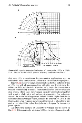
![154 6 Illumination Sources and Techniques
Figure 6.13: Miniature LED HSMC-S690: size compared to an electronic resistor.
Photo taken with an endoscopic optic.
one square millimeter, but shows a luminous intensity of I = 50 mcd
perpendicular to the surface with a total luminous flux of φ = 238 mlm,
which is comparable to the brightest LEDs of larger package sizes. The
intensity distribution is extremely flat and homogeneous. This LED is
extremely useful for illumination purposes, as it can be integrated into
arrays of high density with a corresponding high exitance and homo-
geneity.
There is no general agreement among LED manufacturers and users
as to LED performance specifications, which leads to much confusion
and misunderstanding. In manufacturer literature the most common
quantity given to specify the directional output of an LED is luminous
intensity. This term, however, is very often incorrectly used and the
measured quantity is not the true intensity. In order to measure the
intensity, the flux incident on a detector at a measured distance is used
and the solid angle is computed by dividing the detector area by the
squared distance. In real applications, the distance very often has to
be chosen close to the emitting LED, which might not be large enough
for the emitting area to behave like a point source. If the detector is too
close, the LED acts as an extended source, which corrupts the angular
distribution.
To avoid this problem and to pursue standardization in LED mea-
surements, the international lighting commission, CIE, has defined a
new term, called averaged LED intensity [5]. This term standardizes
close range measurements by specifying the exact distance and size of
the detector used for the measurement. The measurement geometries
will be known as CIE Standard Conditions A and B. For averaged LED
intensities measured under these conditions, the symbols ILED A and
ILED B are recommended. Both conditions involve the use of a detector
with a circular entrance aperture of 100 mm2 (corresponding to a di-](https://image.slidesharecdn.com/computervision-handbookofcomputervisionandapplicationsvolume1-sensorsandimaging-120205081125-phpapp02/85/Computer-vision-handbook-of-computer-vision-and-applications-volume-1-sensors-and-imaging-179-320.jpg)
![6.3 Artificial illumination sources 155
ameter of 11.3 mm). The LED should be positioned facing the detector
and aligned so that the mechanical axis of the LED passes through the
center of the detector aperture. For conditions A and B, the distance d
between the LED and the detector is 316 mm and 100 mm, respectively.
This corresponds to solid angles of 0.001 sr for condition A and 0.01 sr
for condition B. If the detector has been calibrated for illuminance E
the averaged LED intensity can be calculated as
E
ILED = (6.2)
d2
Electrical properties. As the p-n junction of an LED becomes strongly
conducting when operated in forward bias direction, LEDs always have
to be operated with a protective resistance to avoid high currents, which
will destroy the LED by thermal overheating. Currents are typically in
the order of 20 to 50 mA, with a voltage drop across the LED of about
1 V. Thus, the power consumption of LEDs lies in the order of 20 to
50 mW.
As LEDs have very short response times, in the order of microsec-
onds, they can be operated in pulsed mode with variable duty cycles. An
important property of LEDs is the fact that they can be operated above
the current limit for low duty cycle pulses. As the relationship between
optical output and instantaneous forward current is linear over a wide
region, very high intensity peak levels can be reached in pulsed mode.
This technique, however, is not useful with GaP diodes, as they do not
exhibit the linear relationship between current and luminous intensity,
becoming saturated at moderate current levels. The maximum current
depends on the duty cycle, as the average power consumption may not
exceed the critical limit. For detailed information about the maximum
current in dependence of the duty cycle, refer to data sheets provided
by the manufacturer.
The pulsed-mode operation is especially useful for imaging appli-
cations. If LEDs are triggered on the frame sync of the camera signal,
they can be pulsed with the frame rate of the camera. As the integration
time of the camera only subtends a fraction of the time between two
images, the LED output can be optimized by pulsed-mode operation.
In order to operate the LED in pulsed mode, logical TTL-electronics can
be used to generate an LED-pulse from the trigger signal of the cam-
era. This signal can be used to switch the LED via transistors, as the
TTL signal cannot be directly used for power switching of the LED. More
detailed information about TTL electronics and interfaces driving opto-
electronical components with TTL signals can be found in an excellent
handbook on practical electronics by Horowitz and Hill [6].
LED arrays. The small package dimensions and the large variety of
intensity distributions allow LEDs to be integrated into larger arrays](https://image.slidesharecdn.com/computervision-handbookofcomputervisionandapplicationsvolume1-sensorsandimaging-120205081125-phpapp02/85/Computer-vision-handbook-of-computer-vision-and-applications-volume-1-sensors-and-imaging-180-320.jpg)


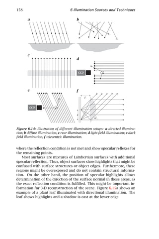
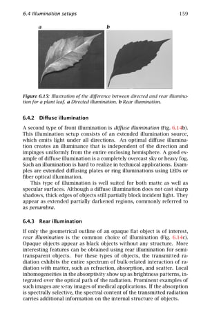


![162 6 Illumination Sources and Techniques
ing species, such as bats and marine mammals, use acoustic signals to
sense their 3-D environment in absolute darkness.
Instead of pulsing the illumination signal, it can also be modulated
with a certain frequency. Examples can be found in scientific applica-
tions. Some processes that are visualized correspond with a certain
time constant upon illumination with specific radiation. For example,
active thermography uses infrared radiation to heat object surfaces and
to observe temporal changes. Using a modulated thermal irradiance,
the time constant of the processes related to the absorption and the
internal transport of heat can be measured.
6.5 References
[1] Wolfe, W. L. and Zissis, G. J. (eds.), (1989). The Infrared Handbook, 3rd
edition. Michigan: The Infrared Information Analysis (IRIA) Center, Envi-
ronmental Research Institute of Michigan.
[2] Carlson, F. E. and Clarke, C. N., (1965). Light sources for optical devices. In
Applied Optics and Optical Engineering, R. Kingslake, ed. New York: Aca-
demic Press.
[3] Oriel Corporation, (1994). Light Sources, Monochromators & Spectrographs,
Detectors & Detection Systems, Fiber Optics, Vol. II. Stratford, CT: Oriel
Corporation.
[4] McCluney, W. R., (1994). Introduction to Radiometry and Photometry.
Boston: Artech House.
[5] CIE, (1997). Measurement of LEDs. CIE, Kegelgasse 27, A-1030 Vienna,
Austria.
[6] Horowitz, P. and Hill, W., (1998). The Art of Electronics. New York: Cam-
bridge University Press.](https://image.slidesharecdn.com/computervision-handbookofcomputervisionandapplicationsvolume1-sensorsandimaging-120205081125-phpapp02/85/Computer-vision-handbook-of-computer-vision-and-applications-volume-1-sensors-and-imaging-187-320.jpg)


![166 7 Solid-State Image Sensing
7.7.6 Digital camera technology . . . . . . . . . . . . . . . . . . 203
7.8 Semiconductor technology for image sensing . . . . . . . . . . 204
7.8.1 Shrinking design rules for more and smaller pixels . 204
7.8.2 Low-cost prototyping . . . . . . . . . . . . . . . . . . . . . 207
7.9 Practical limitations of semiconductor photosensors . . . . . . 207
7.9.1 Pixel nonuniformity and dead pixels . . . . . . . . . . . 207
7.9.2 Sensor nonlinearity . . . . . . . . . . . . . . . . . . . . . . 208
7.10 The future of image sensing . . . . . . . . . . . . . . . . . . . . . . 209
7.10.1 Custom functionality with the photosensor toolbox . 210
7.10.2 Smart image sensors . . . . . . . . . . . . . . . . . . . . . 215
7.10.3 On the way to seeing chips? . . . . . . . . . . . . . . . . . 217
7.11 Conclusions . . . . . . . . . . . . . . . . . . . . . . . . . . . . . . . . 218
7.12 References . . . . . . . . . . . . . . . . . . . . . . . . . . . . . . . . . 219
7.1 Introduction
As the name indicates, the field of computer vision has long been viewed
as an essentially computational science, concerned only with the mathe-
matical treatment of images whose origins are effectively ignored. This
conventional view of computer vision (or machine vision), as perceived,
for example, in the textbook by Gonzalez and Wintz [1], has slowly
given way to a different, holistic comprehension of machine vision as
the science of systems that extract information from wave fields (see
also Chapter 1 or, for a practical implementation, Chapter 16). This
systems approach, sometimes also called electronic imaging [2], has
two immediate consequences: first, in a well-designed system, different
components can compensate for the deficiencies in other components;
practical examples of this capability include the digital correction of
imaging lens distortions in photogrammetric applications (Chapter 17
or [3]), the significant increase of a system’s dynamic range by nonlin-
ear compression of the photosignal in the image sensor (Chapter 8 or
[4]), and the digital compensation of offset and gain nonuniformities
in the image sensor [5]. Second, the image acquisition process can be-
come dynamic and adaptive, reacting to changes in the outside world
by adapting the properties of the image capture and processing compo-
nents in an optimal fashion. This powerful concept of active vision has
already been proposed previously [6] but only now, with the recent de-
velopment of custom solid-state image sensors, is it possible for active
vision to reach its full potential, as described, for example, in Volume 3,
Chapter 9. At the same time, new research opportunities are occurring
in machine vision because new types of image processing algorithms
are required that not only influence the image acquisition process but
are also capable of exploiting novel imaging modalities [7].](https://image.slidesharecdn.com/computervision-handbookofcomputervisionandapplicationsvolume1-sensorsandimaging-120205081125-phpapp02/85/Computer-vision-handbook-of-computer-vision-and-applications-volume-1-sensors-and-imaging-191-320.jpg)

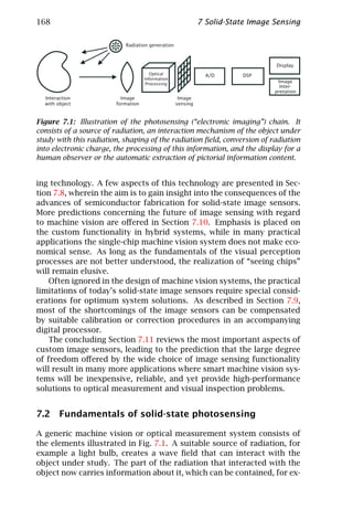

![7.2 Fundamentals of solid-state photosensing 171
100
Absolute quantum efficiency [%]
80
60
40
20
400 600 800 1000
Wavelength [nm]
Figure 7.4: Absolute quantum efficiency measurement of a silicon p-n junction
realized with a standard CMOS process. This example illustrates the decay to-
wards the blue (surface absorption) and red spectral region (interaction too deep
in the semiconductor), as well as the oscillations due to thin-film interference.
is obtained in the following way: using an index of refraction of
n=1.5 for silicon dioxide, 4 % of the photons are reflected at normal
incidence from air [8].
2. Multiple reflections in the covering thin layer lead to a strong spec-
tral oscillation of the transmittance, as is apparent in the measure-
ment shown in Fig. 7.4.
Depending on the wavelength of the incident photon it is either
transmitted well or it is preferentially reflected back. In good image
sensors, this disturbing effect is virtually eliminated by the deposi-
tion of additional dielectric antireflection layers on top of the image
sensor [8].
3. The covering layers are not perfectly transparent, leading to absorp-
tion of part of the incident photons already at this stage. The re-
duced blue response of CCD image sensors is a good example of
this effect, caused by the low transmission of the covering polysili-
con electrodes on the pixels.
4. Inactive regions near the surface of the semiconductor consist of
semiconductor material with a very short lifetime of charge pairs.
This is either caused by defects right at the interface (less than 1 nm),
or by very high doping concentration near contacts [9]. Photogen-
erated charge pairs recombine so fast that their collection and elec-
tronic detection is improbable.
5. Photons that are absorbed very deeply in the bulk of the semicon-
ductor result in photocharge that does not have a chance to reach
the surface of the image sensor for collection in a pixel. As will be](https://image.slidesharecdn.com/computervision-handbookofcomputervisionandapplicationsvolume1-sensorsandimaging-120205081125-phpapp02/85/Computer-vision-handbook-of-computer-vision-and-applications-volume-1-sensors-and-imaging-196-320.jpg)
![172 7 Solid-State Image Sensing
photon energy (eV)
6
3 2.5 1 0.75 -2
light penetration depth 1/α (µm)
10 10
absorption coefficient α (cm )
300 K
-1
Ge(λ=1.24/E=1.88 µm)
5 g -1
10 10
4
10 1
Si(1.1 µm) GaAs(0.9 µm)
3 1
10 10
2 a-Si(0.8 µm) 2
10 10
0.2 0.6 1 1.4 1.8
wavelength (µm)
Figure 7.5: Optical absorption coefficient and light penetration depth as a func-
tion of wavelength for various semiconductor materials. Data taken from Sze
[10].
described in what follows, the critical distance is the so-called diffu-
sion length L, which can be many times 10 µm deep for low-doped
semiconductors [9].
6. Finally, photons might travel through the image sensor without in-
teraction, leaving it again at the back end.
7.2.2 Generation of photocharge pairs
Because of the sequential process of photocharge generation, virtually
all photons that are absorbed in the semiconductor material are con-
verted into an electronic charge [8]. There is a strong spectral depen-
dence, however, of the mean absorption depth at which this photocon-
version takes place, as illustrated in Fig. 7.5. Short-wavelength light
is predominantly absorbed at the surface, while red light penetrates
deeply into the bulk of the semiconductor. A major consequence of this
effect is that the achievable spatial resolution degrades significantly
with wavelength [11]: images taken in the red or infrared spectral re-
gion show much less contrast compared to images taken in green or
blue light. For this reason, image sensors are often covered with an
optical filter, cutting off the infrared portion of the incident light.
In the absorption process, a photon loses its energy by creating one
or more charge pairs. In a photodetection event, no net charge is cre-
ated and neutrality is always maintained. For this reason, charge pairs
are created, consisting of an electron and a (positively charged) quasi-
particle called hole [8]. The overall charge conversion efficiency of this
process is usually measured with the quantum efficiency η, describing
how many charge pairs are created and electronically detected per inci-
dent photon. Alternatively, this conversion efficiency can be described](https://image.slidesharecdn.com/computervision-handbookofcomputervisionandapplicationsvolume1-sensorsandimaging-120205081125-phpapp02/85/Computer-vision-handbook-of-computer-vision-and-applications-volume-1-sensors-and-imaging-197-320.jpg)
![7.2 Fundamentals of solid-state photosensing 173
with the responsivity R in units A/W, measuring how much current is
flowing out of a photosensor per incident light power. The relationship
between R and η is given by
λq
R=η (7.1)
hc
Using Planck’s constant h, the speed of light c, the unit charge q, and
the photons’ wavelength λ. As an example, consider a photodetector
with an η of 0.9, illuminated with red light (λ =633 nm) from a HeNe
laser. The corresponding responsivity is R =0.46 A/W.
In the visible and infrared portion of the spectrum, η is less than
unity. This is illustrated in Fig. 7.4 with the actual measurement of an
n− p− photodiode, manufactured with a standard CMOS process using
silicon. The η decreases towards both the blue (incident light is al-
ready absorbed in the covering layers) and the infrared portion of the
spectrum (light penetrates and interacts so deeply in the semiconduc-
tor that the created charge pairs recombine and disappear before they
reach the surface where they could have been collected and measured).
In the visible part of the spectrum, a rather high η of close to 100 % is
observed. As no special antireflection coating is used in this photodi-
ode, spectral oscillations can be seen in the η curve, caused by multiple
reflections of the incident light within the covering layers [8], so-called
thin-film interference. For improved performance, antireflection coat-
ings are employed, reducing this effect significantly.
If a photon has a sufficiently high energy such as in x-rays, one pho-
ton can create many charge pairs. In silicon a mean energy of 3.8 eV is
required for the creation of one electron-hole pair [12]. As an example,
consider a soft x-ray photon with an energy of 1000 eV, correspond-
ing to a wavelength of 1.24 nm. The absorption of this x-ray photon
results in the creation of 263 charge pairs. Because silicon starts to be-
come transparent for x-ray photons with an energy of more than a few
1000 eV, silicon is not an efficient solid state detector for such energies.
Other semiconductors, consisting of high-density materials with atoms
of high atomic numbers, are more appropriate for x-ray detection [13].
7.2.3 Separation of photogenerated charge pairs: photocurrents
Once a charge (electron-hole) pair has been created, it must be sep-
arated within a certain time before it recombines again and loses all
information about the previous presence of the photon that generated
the charge pair. This recombination lifetime τ depends critically on
the quality and purity of the semiconductor [9]. In high-quality low-
doped silicon used in CMOS processes, for example, the lifetime can be
as large as several tens of microseconds. This is the time available for](https://image.slidesharecdn.com/computervision-handbookofcomputervisionandapplicationsvolume1-sensorsandimaging-120205081125-phpapp02/85/Computer-vision-handbook-of-computer-vision-and-applications-volume-1-sensors-and-imaging-198-320.jpg)
![174 7 Solid-State Image Sensing
separating the photocharge and moving the different charge types to
suitable storage areas.
Two physical effects dominate the motion of electronic charge in
semiconductors: drift in an electric field and diffusion caused by the
random thermal motion of the charge carriers. The presence of an
electric field E causes charge carriers to move with the velocity v
v = µE (7.2)
with the mobility µ. As an example, the mobility of electrons in low-
doped silicon at room temperature is about 1350 cm2 /Vs. Above a
certain field strength, the velocity saturates, taking on a constant value
vsat . For silicon, this saturation velocity is about 105 m/s [10].
Even in the absence of an electric field, charge can move: the thermal
random motion causes diffusion, a tendency of charge carriers to equi-
librate their distribution. The thermally induced velocity vdiff of the
charge carriers can be very high: an electron at room temperature has
an average velocity of vdiff = 105 m/s. This random motion causes an
average [root-mean-square (rms)] displacement L of a single electron,
depending on the time t given for the diffusion process
L = Dt (7.3)
with the diffusion constant D. Silicon exhibits a typical electron dif-
fusion constant of about 45 cm2 /s at room temperature. For the re-
combination lifetime τ already mentioned, the corresponding average
displacement L is called diffusion length. This is the average distance
over which a charge carrier can move without the influence of an elec-
tric field and without recombining. As an example, consider τ = 10 µs
and D =45 cm2 /s, resulting in L =212 µm. This implies that the diffu-
sion process can be extremely important for the collection of charge
carriers over significant distances. This also means that charge carri-
ers photogenerated deeply in the semiconductor have a high chance
of reaching the surface, where they can be collected and where they
contribute to a severe reduction of the contrast, especially for small
pixel periods. As mentioned in the preceding, this can be counteracted
only by filtering out the long-wavelength photons that would penetrate
deeply into the semiconductor.
Photogenerated charge carriers moving under the influence of an
electric field represent a current, the so-called photocurrent . This pho-
tocurrent is proportional to the incident light intensity over 10 orders
of magnitude and more [14]. It is this strict linearity of photocurrent
with incident light over a wide dynamic range that makes semiconduc-
tor photosensors so attractive for many applications in image sensors
and optical measurement systems.](https://image.slidesharecdn.com/computervision-handbookofcomputervisionandapplicationsvolume1-sensorsandimaging-120205081125-phpapp02/85/Computer-vision-handbook-of-computer-vision-and-applications-volume-1-sensors-and-imaging-199-320.jpg)
![7.3 Photocurrent processing 175
a b
conductor conductor
n+ oxide
channel
p+ s top
space-charge region space charge
p-type silicon substrate p-type silicon substrate
Figure 7.6: Cross sections through the two major types of electrical field gener-
ating and charge storing devices in semiconductors: a photodiode, consisting of
a reverse-biased p-n junction; b MOS capacitance, consisting of a (transparent)
electrode on the semiconductor material, separated by a dielectric insulation.
7.3 Photocurrent processing
All the information a photosensor can extract from the light distribu-
tion in a scene is contained in the spatial and temporal modulation of
the photocurrent in the individual pixels. For this reason, it is of much
interest to process the pixels’ photocurrents accordingly, in order to ob-
tain the relevant modulation parameters in the most efficient manner
[7]. Traditionally, only the integrated photocurrent could be extracted;
today a large variety of photocurrent preprocessing is available, mak-
ing it possible to optimize the photosensor acquisition parameters to a
given problem. In the following, a few examples of such photocurrent
preprocessing are presented.
7.3.1 Photocharge integration in photodiodes and charge-coupled
devices
The simplest type of photocurrent processing is the integration of the
photocurrent during a certain time, the exposure time. In this way
an integrated charge is obtained that is proportional to the number of
photons incident on the pixel’s sensitive area during the exposure time.
This functionality is very easy to implement by employing the capaci-
tance of the device used for generating the electric field for photocharge
separation. Figure 7.6 illustrates this principle for the two most impor-
tant photosensitive structures, the photodiode (PD) and the metal-oxide-
semiconductor (MOS) capacitor as used in the charge-coupled device
(CCD) image sensors. Both devices are easily fabricated with standard
semiconductor processes.](https://image.slidesharecdn.com/computervision-handbookofcomputervisionandapplicationsvolume1-sensorsandimaging-120205081125-phpapp02/85/Computer-vision-handbook-of-computer-vision-and-applications-volume-1-sensors-and-imaging-200-320.jpg)
![176 7 Solid-State Image Sensing
A photodiode consists of a combination of two different conductiv-
ity types of semiconductor, as illustrated in Fig. 7.6a. In the junction be-
tween the two types of semiconductor, an electric field in the so-called
space-charge region exists, as required for the separation of photogen-
erated charge carriers. At the same time, this space-charge region has a
certain capacitance, varying with the inverse of the space-charge region
width. Photodiodes are typically operated by biasing (“resetting”) them
to a certain potential and exposing them to light. Photocharge pairs en-
tering the space-charge region are separated in the PD’s electric field,
a photocurrent is produced, and the photocharge is accumulated on
the PD’s capacitance, lowering the voltage across it. After the exposure
time, the residual voltage is measured, and the voltage difference com-
pared with the reset voltage level is a measure for the amount of light
incident on the pixel during the exposure time.
The MOS-capacitance illustrated in Fig. 7.6b consists of a thin layer
of oxide on top of a piece of semiconductor. The oxide is covered with
a conductive material, often a metal or highly doped polycrystalline
silicon (polysilicon). As in the case of the PD, the MOS structure is
biased to a suitable voltage, leading to a space-charge region of a certain
extent in the semiconductor. Again, photocharge is separated in the
electric field and it is integrated on the MOS capacitance, collected at
the interface between semiconductor and oxide.
A typical value for the PD and MOS area capacitance is 0.1 fF/µm2 .
Assuming a maximum voltage swing of a few volts, this implies a stor-
age capacity of a few thousand photoelectrons per µm2 . Once this stor-
age capacity is exceeded, additional photocharge in the corresponding
pixel starts to spill over to neighboring pixels. This effect is called
blooming, and well-designed image sensors provide special collecting
(“antiblooming”) structures for a reduction of this effect [15].
7.3.2 Programmable offset subtraction
Several machine vision and optical metrology problems suffer from
small spatial contrast [7]. In such cases in which the spatial signal
modulation is small compared to the background light level, one would
profit from an offset subtraction mechanism in each pixel. This can be
realized, even programmable in each pixel, with the offset subtraction
mechanism proposed by Vietze and Seitz [16]. Each pixel contains a
photodiode in series with a programmable current source, as illustrated
in Fig. 7.7. This current source is easily realized with a MOSFET, whose
gate voltage can be preset to a certain voltage level with a second MOS-
FET, and by using a capacitance for the storage of this gate voltage. The
MOSFET is operated in the so-called weak-inversion regime, where the
drain current depends exponentially on the gate voltage; the current
typically doubles with each increase of gate voltage by about 30 mV. In](https://image.slidesharecdn.com/computervision-handbookofcomputervisionandapplicationsvolume1-sensorsandimaging-120205081125-phpapp02/85/Computer-vision-handbook-of-computer-vision-and-applications-volume-1-sensors-and-imaging-201-320.jpg)
![7.3 Photocurrent processing 177
V C V reset V
program M
M
M M
reset M
Figure 7.7: Schematic diagram of the offset pixel with current source transistor
Mcur , reset transistor Mr , row-select transistor Msel , and sense transistor Ms .
The value of the offset current is stored on the switched offset memory capacitor
CM with the programming switch Mp [16].
a b
Figure 7.8: Application example of the offset pixel—motion detector realized
with a 26 × 28 pixel CMOS image sensor [17]: a sensor image of a simple scene
(black letters “PSI” on white paper) after adjusting the pixels’ individual offset
current to a medium gray level; b sensor image after moving the scene slightly
downwards and to the right. Pixels with changed values appear either black or
white.
this way, the offset current can be varied easily between 1 fA up to sev-
eral tens of µA [17]. The same integration mechanism as presented in
Section 7.3.2 is employed for the collection of signal photocharge, rep-
resenting the difference between total photocharge minus offset pho-
tocharge. Using this method, a dynamic range exceeding 150 dB can be
reached, and several interesting applications can be realized very eas-
ily. An example of this is a simple change detector , implemented as a
two-stage process. In a first stage, the offset current in each pixel is pro-
grammed such that the net result is zero; the offset currents effectively
cancel the local photocurrents. In a second stage, the image is simply
observed for non-zero pixels, indicating that there was a change in the
present scene compared to the original “reference” scene: a change in
the scene has occurred!](https://image.slidesharecdn.com/computervision-handbookofcomputervisionandapplicationsvolume1-sensorsandimaging-120205081125-phpapp02/85/Computer-vision-handbook-of-computer-vision-and-applications-volume-1-sensors-and-imaging-202-320.jpg)
![178 7 Solid-State Image Sensing
VDD Vreset VDD
reset
Vdiff
select
out
Figure 7.9: Schematic diagram of the gain pixel, consisting of a modified cur-
rent mirror [17], with which a photocurrent multiplication with a factor ranging
between 10 −4 up to more than 10 4 can be realized.
The realization of such a change detector is illustrated with an ex-
perimental offset pixel image sensor with 28 × 26 pictures, fabricated
with standard CMOS technology [17]. In Fig. 7.8a the result of offset
cancellation for a stationary scene containing the letters PSI is shown:
a uniform gray picture. Once the object is moved (the letters are shifted
downwards), the resulting pixels appear as bright where the dark object
was, or as dark where the bright background was, see Fig. 7.8b.
7.3.3 Programmable gain pixels
Another local operation desirable in an image sensor is the individual
multiplication of the photocurrent with a programmable factor. This
can be achieved with a modification of a simple electronic circuit called
current mirror , consisting of two transistors. In the standard configu-
ration, the gate terminals of the two transistors are connected. In the
modification proposed in Vietze [17], a voltage difference between the
two gates is applied, as illustrated in Fig. 7.9. This voltage difference is
either fixed (e.g., by semiconductor process parameters), or it can be im-
plemented as individually programmable potential differences across a
storage capacitor. The photocurrent produced by a photodiode in the
first branch of the modified current mirror results in current in the sec-
ond branch that is given by the photocurrent times a factor. By using a
similar physical mechanism as in the offset pixel, the gain pixel shows a
current doubling (or halving) for each increase (decrease) of the voltage
difference by about 30 mV. In this way, current multiplication (division)
by several orders of magnitude can easily be obtained. As before, the
multiplied photocurrent is integrated on a storage capacitor and read
out using conventional circuitry.
An application of this is a high-sensitivity image sensor as described
in [17], in which each pixel has a fixed gain of about 8500. In this way,
a sensitivity (see Section 7.5.1 for the definition) of 43 mV per photo-](https://image.slidesharecdn.com/computervision-handbookofcomputervisionandapplicationsvolume1-sensorsandimaging-120205081125-phpapp02/85/Computer-vision-handbook-of-computer-vision-and-applications-volume-1-sensors-and-imaging-203-320.jpg)
![7.3 Photocurrent processing 179
electron has been obtained, and an input-referred rms charge noise of
better than 0.1 electrons at room temperature. As will be discussed
in Section 7.5, this impressive performance must come at a price. In
this case it is the reduced bandwidth of the pixel, reflected in the low-
pass filter characteristics at low photocurrents with response times of
several milliseconds.
7.3.4 Avalanche photocurrent multiplication
The multiplication mechanism described in the foregoing is based strict-
ly on the use of electronic circuitry to achieve gain. In semiconductors
there is a physical mechanism that can be exploited to multiply charge
carriers before they are detected. This effect is called avalanche multi-
plication, and it is used in so-called avalanche photodiodes (APDs) [18].
If the electric field is increased to a few times 105 V/cm, charge carriers
are multiplied with a strongly field-dependent factor. Depending on the
specific doping conditions in the semiconductor, the necessary electric
fields correspond to breakdown voltages between a few volts and a few
hundred volts. The strong dependency of the multiplication factor on
voltage is illustrated with a model calculation for a breakdown voltage
of 40 V, shown in Fig. 7.10 [19].
The APDs are commercially available and, because of the high achiev-
able gains, they are even suitable for single-photon light detection [20].
Due to the unusual voltages, the complex voltage stabilization/homoge-
nization circuits and the nontrivial readout electronics in each pixel,
most APDs are only of the single-pixel type. The development of APD
line and image sensor arrays has only just started. Nevertheless, the
fabrication of reliable APD image sensors with CMOS processes is an
active topic of research, and promising results have already been ob-
tained (see, for example, Mathewson [21].
7.3.5 Nonlinear photocurrent to signal voltage conversion
Image processing algorithms are often motivated by solutions found
in biological vision systems. The same is true for different types of
photodetection strategies, especially for the realization of image sen-
sors offering a similarly large dynamic range already inherent in ani-
mal vision. The fact that the human eye shows a nonlinear, close to
logarithmic sensitivity has been exploited, for example, in the artifi-
cial retina described in Mahowald [22]. The realization of CMOS pixels
offering a logarithmic sensitivity is particularly easy to achieve: one
can use the logarithmic relationship between gate voltage and drain
current in a MOSFET operated in weak inversion, already described in
Section 7.3.2. The resulting pixel architecture, shown in Fig. 7.11 and
exploited in Chapter 8, is particularly easy to implement in a CMOS](https://image.slidesharecdn.com/computervision-handbookofcomputervisionandapplicationsvolume1-sensorsandimaging-120205081125-phpapp02/85/Computer-vision-handbook-of-computer-vision-and-applications-volume-1-sensors-and-imaging-204-320.jpg)
![180 7 Solid-State Image Sensing
1000 1000
Avalance multiplication gain
Breakdown voltage = 40 V
Exponential factor = 4
100 100
10 10
1 1
0 10 20 30 40
Voltage [V]
Figure 7.10: Empirical relationship between applied voltage and obtained cur-
rent gain in an avalanche photodiode, for which a breakdown voltage of VB = 40
V and an exponent of n =4 have been assumed.
V
Mlog Msense
select Msel
Figure 7.11: Schematic diagram of a pixel with logarithmic response, consist-
ing of just one photodiode and three MOSFETs. Implemented with a standard
CMOS process, such a pixel shows an output voltage increase of about 40 mV
per decade of incident light power.
process because a pixel consists of just a photodiode and three MOS
transistors [23]. A typical photoresponse of about 40 mV per decade of
optical input power is obtained with such logarithmic pixels, and their
useful dynamic range exceeds 120 dB. Practical examples of scenes re-
quiring such a high dynamic range are illustrated in Fig. 7.12, with the
actual measurements taken with a logarithmic image sensor exhibiting
64 × 64 pixels. In the image of a light bulb, the glowing filament as well
as the background are clearly visible at the same time. Back-illuminated
scenes, such as a portrait in front of a window, are dreaded by photog-](https://image.slidesharecdn.com/computervision-handbookofcomputervisionandapplicationsvolume1-sensorsandimaging-120205081125-phpapp02/85/Computer-vision-handbook-of-computer-vision-and-applications-volume-1-sensors-and-imaging-205-320.jpg)

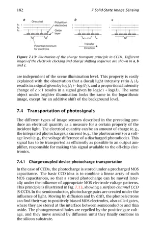
![7.4 Transportation of photosignals 183
It is important to note that a CCD pixel is not represented only by
the positively biased gate because this electrode can receive diffusing
and drifting photoelectrons from its environment. A pixel’s geometry
is therefore rather defined in terms of “effective photocharge collection
area,” extending about halfway to the next positively biased electrode.
This also shows that a pixel does not have sharply defined edges; the
extent of the charge collection area representing a pixel depends on
the wavelength, the electric field distribution, and the diffusion prop-
erties of the semiconductor. Generally, longer wavelength light results
in a lower contrast and offers reduced resolution, as discussed in Sec-
tion 7.2.2.
In Fig. 7.13, the potential distribution under the electrodes right at
the surface is indicated. Photocharge accumulates in the shown “po-
tential wells.” By changing the gate voltage patterns, the potential wells
can be widened, leading to a broadened distribution of photoelectrons.
Using a suitable gate voltage pattern, one can also reduce the extent of
the potential wells, and photoelectrons move again to regions with the
lowest potential. As illustrated in Fig. 7.13, it is physically possible to
transport photocharge. This transport mechanisms works rather well
up to frequencies of a few MHz. In good S-CCDs, only about 0.01 % of the
photocharge is lost on average in transporting a photoelectron packet
from one gate to another, neighboring gate. Instead of this charge
transport loss, one often uses the charge transfer efficiency (CTE) con-
cept, defined as the complement to 100 %. The CTE amounts to 99.99 %
in the case of a good S-CCD.
In long CCD lines, a CTE of 99.99 % is still not good enough. Charge
is trapped at the surface, making it hard to improve the CTE. For this
reason, another type of CCD has been invented, the buried-channel CCD
(B-CCD), in which the transport takes place in the bulk of the semicon-
ductor, a few 100 nm away from the surface. Those CTEs of up to
99.99995 % can be obtained in B-CCDs, and all commercially available
CCD line and image sensors are of this type.
Above a limiting clock frequency a CCD’s CTE starts to degrade
rapidly. Nevertheless, CCDs have been operated successfully at very
high clock frequencies. For silicon, 1 GHz has been achieved [24], while
GaAs CCDs have reached 18 GHz clocking frequency [25]. Such high
clock rates require special precautions in the CCD fabrication process,
usually not available for standard video sensors. Today’s technology
limits the analog bandwidth of CCDs to about 40 MHz. This is suffi-
cient for standard video imagers according to the European CCIR or the
American RS-170 black-and-white video standard. For HDTV sensors,
however, the required pixel rate is around 75 MHz, making it necessary
to operate two outputs in parallel in HDTV CCD imagers.](https://image.slidesharecdn.com/computervision-handbookofcomputervisionandapplicationsvolume1-sensorsandimaging-120205081125-phpapp02/85/Computer-vision-handbook-of-computer-vision-and-applications-volume-1-sensors-and-imaging-208-320.jpg)

![7.5 Electronic signal detection 185
ter characteristics results in voltage noise that is proportional to one
over the square root of the video line’s capacitance [26]. The larger this
capacitance, the lower the voltage noise. For this reason, voltage signals
can be transmitted with much less noise and higher measurement pre-
cision than (small) charge signals. This implies that image sensor types
offering voltage transmission architectures, such as that provided by
the logarithmic pixel described in Section 7.3.5, have an inherent noise
advantage over conventional PD architectures. This will be discussed
in more detail in Section 7.3.3.
7.5 Electronic signal detection
The basic task of electronic signal detection is the precise measure-
ment of voltage signals offering low noise levels and a wide dynamic
range. These input voltage signals have either been produced by the
conversion of photocharge into a voltage, for example by employing a
capacitance, or they are the result of more elaborate photocharge pre-
processing as was already described here. The output of the signal
detection electronics is usually a voltage that should be proportional
to the input voltage over a large dynamic range. An important property
of the signal detection electronics is that its output should have very
low impedance, that is, the output voltage should be stable and must
not depend on the amount of current drawn. As we will see in what
follows, the electronic signal detection noise is today’s limiting factor
in increasing an image sensor’s sensitivity and its dynamic range.
7.5.1 Signal-to-noise and dynamic range
For a numerical description of the voltage or charge-noise performance
of an electronic circuit, two values are often used, the signal-to-noise
ratio SNR and the dynamic range DR. The SNR is defined by comparing
an actual signal level V with its rms noise ∆V , according to:
V
SNR = 20 10 log (7.4)
∆V
The DR compares the maximum signal level ∆vmax with the mini-
mum rms noise level (∆Vmin , in an image sensor typically obtained in
the dark
Vmax
DR = 20 10 log (7.5)
∆Vmin
As an example, consider a CCD image sensor whose maximum charge
(“full well charge”) is 50,000 electrons, and for which a dark noise of](https://image.slidesharecdn.com/computervision-handbookofcomputervisionandapplicationsvolume1-sensorsandimaging-120205081125-phpapp02/85/Computer-vision-handbook-of-computer-vision-and-applications-volume-1-sensors-and-imaging-210-320.jpg)
![186 7 Solid-State Image Sensing
VD VD
Vg Msense Vg Msense
C C
Vf Vf
Rload Vbias Mload
Figure 7.14: Schematic diagram of the source follower circuit realized with a
resistor (left) or with a so-called active load MOSFET (right). This is the most
often used electronic circuit for photocharge detection in semiconductor image
sensors. Photocharge deposited on the gate capacitance leads to a gate voltage
Vg , which in turn produces a linear change in output voltage Vf .
50 electrons rms is observed. This image sensor has a dynamic range
of 60 dB.
It should be mentioned that the preceding definitions of SNR and
DR in image sensors are not consistent with usage elsewhere in opti-
cal physics: as the measured voltage at the image sensor’s output is
usually proportional to the incident optical power, a factor of 10 in
front of the logarithm should be used instead of the employed factor
20. However, because electrical engineers are used to associate power
only with the square of voltage levels, the definitions given here are the
ones employed almost exclusively for all image sensor specifications.
7.5.2 The basic MOSFET source follower
Although elaborate circuits exist for the desired conversion of volt-
age signals into other voltage signals, most image sensors employ the
simplest type of voltage measurement circuits, the MOSFET source fol-
lower . As shown in Fig. 7.14, this circuit consists of just one transis-
tor and one resistor, which is often implemented as another transistor
called active load [27]. The output voltage of this source follower circuit
is essentially given by
Vout = f Vin − V0 (7.6)
with a transistor-dependent multiplication factor f of 0.6-0.8 and an
offset voltage V0 of several hundred millivolts. In practice, one or
a few such source follower stages are employed in series, to obtain
low enough output impedance while maintaining the required read-out
speed. At first sight it is surprising that such a simple circuit with a](https://image.slidesharecdn.com/computervision-handbookofcomputervisionandapplicationsvolume1-sensorsandimaging-120205081125-phpapp02/85/Computer-vision-handbook-of-computer-vision-and-applications-volume-1-sensors-and-imaging-211-320.jpg)
![7.5 Electronic signal detection 187
Vreset VD
reset
Mreset
Msense
C
output Vout
diffusion
Vbias Mload
Figure 7.15: Complete single-stage output circuit of a typical image sensor,
consisting of a floating diffusion, a reset transistor, and a single-stage source
follower as shown in Fig. 7.14.
gain of less than unity is used in high-sensitivity image sensors. The
reason for this is that the photocharge conversion gain is provided by
the effective input capacitance, which is kept as small as possible. To-
day’s best image sensors have an effective input capacitance of around
15 fF, corresponding to a voltage increase of around 10 µV per electron.
Taking the circuits’ overall gain of less than unity into account, one ar-
rives at the so-called sensitivity of the image sensor, expressed in µV
per electrons. Typical sensitivities of state-of-the-art CCD and CMOS
image sensors are between 5 and 10 µV per electron.
7.5.3 Noise sources in MOSFETs
Based on a source follower circuit, a typical output stage of an image
sensor consists of the components shown in Fig. 7.15. The photocharge
is transported to a diffusion (either the output diffusion of a CCD or the
photodiode itself) that is connected to the gate of the source-follower
MOSFET. Before measurement of each individual photocharge packet,
the diffusion and the connected gate are biased to a reference voltage
using a so-called reset MOSFET. Three main noise sources can be iden-
tified in such a circuit [26], whose influences are referenced back to the
input of the source-follower MOSFET, contributing to an effective rms
charge measurement uncertainty ∆Q.
Reset or kTC noise. The channel of the reset transistor exhibits John-
son noise similar to an ordinary resistor. This causes statistical fluc-
tuations in the observed reset voltage levels, which result in effective
charge noise ∆Qr eset given by
∆Qr eset = kT C (7.7)](https://image.slidesharecdn.com/computervision-handbookofcomputervisionandapplicationsvolume1-sensorsandimaging-120205081125-phpapp02/85/Computer-vision-handbook-of-computer-vision-and-applications-volume-1-sensors-and-imaging-212-320.jpg)
![188 7 Solid-State Image Sensing
for the effective input capacitance C, at the temperature T and using
Boltzmann’s constant k.
Flicker or 1/f noise. Statistical fluctuations in the mobility and charge
carrier concentration of the source follower transistor’s channel cause
an effective charge noise ∆Qf licker described by
IAB
∆Qf licker ∝ C 2
(7.8)
gm f Cox W L
at frequency f , for current I, bandwidth B, transistor length L, and
width W , oxide capacitance Cox , process-dependent flicker noise con-
stant A, which is typically between 0.5 and 2, and the transistor’s trans-
conductance gm .
Thermal noise. Johnson noise in the source follower transistor’s chan-
nel can also be referred back to the input, resulting in thermally gener-
ated charge noise ∆Qther mal given by
4kT Bα
∆Qther mal = C (7.9)
gm
using the same parameters as in the preceding.
In practice, the first two noise sources can be essentially eliminated
by a signal-processing technique called correlated double sampling (CDS)
[28]: reset noise is canceled by a two-stage process, in which the diffu-
sion is preset to a reference voltage and a first measurement is made of
this voltage level. In a second step, the photocharge is transferred to
the diffusion, and a second measurement is made. The difference be-
tween these two measurements is free of reset noise and contains only
information about the photocharge of interest. Because CDS is a tem-
poral high-pass filter, flicker noise with its low-frequency dominance is
effectively canceled at the same time.
The thermal noise contribution cannot be reduced using signal-proc-
essing techniques, and it is obvious from Eq. (7.9) what can be done to
minimize thermal noise. Reduction of temperature (in astronomical
applications down to -120 °C) not only lowers charge noise levels [29]
but the dark current contribution can be reduced to values as low as
one electron per day per pixel. As a rule of thumb, dark current in
silicon doubles for each increase in temperature of around 8–9 °C.
Often the reduction in temperature is combined with a reduction of
the readout bandwidth to 50–100 kHz, leading to a charge noise level of
around one electron [30]. Another technique of bandwidth reduction is
the repetitive, nondestructive measurement of photocharge with out-
put signal averaging, as carried out in the Skipper CCD [31]. Charge](https://image.slidesharecdn.com/computervision-handbookofcomputervisionandapplicationsvolume1-sensorsandimaging-120205081125-phpapp02/85/Computer-vision-handbook-of-computer-vision-and-applications-volume-1-sensors-and-imaging-213-320.jpg)
![7.6 Architectures of image sensors 189
noise levels of 0.3 electrons rms have been obtained in this way. As
can be seen in Eq. (7.9) the dominant factor in noise performance is
the effective input capacitance. This has been lowered to values of less
than 1 fF using the so-called double-gate MOSFET [32], corresponding
to a sensitivity of more than 200 µV per electron and an effective charge
noise level of less than one electron at room temperature and at video
frequencies. As the maximum photocharge such an output stage can
handle is about 10,000 electrons, the DR is limited to about 80 dB.
7.6 Architectures of image sensors
For the acquisition of 1-D and 2-D distributions of incident light, arrays
of pixel are required. Such arrays can be realized as an arrangement
of CCD columns or as suitably placed and interconnected individual
photodiodes as described in Section 7.3.1. Depending on the choice
of arrangement and interconnection, different types of image sensors
result.
7.6.1 Frame-transfer charge-coupled devices
The simplest type of CCD image sensor is the frame-transfer (FT) CCD.
As illustrated in Fig. 7.16, it consists of three CCD sections. One CCD
area (A register) is used for the conversion of photons into photocharge
during the exposure time and for the storage of this photocharge in the
pixels. This 2-D photocharge distribution is subsequently shifted down
into another CCD area (B register), which is covered with an opaque
metal shield. From the B register, an image row at a time is shifted
down into a CCD line (C register), with which the photocharges are
transported laterally to the output amplifier, so that the content of this
image row can be accessed sequentially.
The disadvantage of the FT-CCD principle is the after-exposure of
bright areas that can occur when the photocharge pattern is trans-
ported from the A register into the light-shielded B register. This oc-
curs because the A register remains light-sensitive during the vertical
photocharge transportation time. The after-exposure effect in FT-CCDs
can create saturated (“bright”) columns without any contrast informa-
tion. For this reason, high-quality FT-CCD cameras employ a mechani-
cal shutter, shielding the A register from incident light during the ver-
tical photocharge transportation time.
The big advantage of the FT-CCD is that the whole A register area
is photosensitive; one speaks of an optical fill factor of 100 %. Because
the A register is covered with polysilicon CCD electrodes that tend to
absorb in the blue and UV, an FT-CCD is not very sensitive in the blue
spectral region. For special applications this can be remedied by thin-](https://image.slidesharecdn.com/computervision-handbookofcomputervisionandapplicationsvolume1-sensorsandimaging-120205081125-phpapp02/85/Computer-vision-handbook-of-computer-vision-and-applications-volume-1-sensors-and-imaging-214-320.jpg)
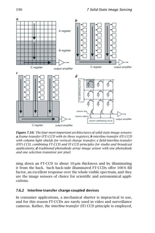

![192 7 Solid-State Image Sensing
termediate storage register. The sequential row-by-row readout is then
effectuated from the B and C registers, exactly as in FT-CCDs.
7.6.4 Conventional photodiode (MOS) arrays
A photodiode or MOS array image sensor consists of a 1-D or 2-D ar-
rangement of PDs, each provided with its own selection transistor, as
illustrated in Fig. 7.16d. For a description of the PD image sensor’s
operation, assume that all PDs are precharged to a certain reverse bias
voltage, typically 5 V. Under the influence of the incident light, each
pixel is discharged to a certain level. A pixel is read out by addressing
the corresponding row and column transistors, providing a conducting
line from the pixel to the output amplifier. Using this line the pixel is
charged up again to the same reverse bias voltage as before. The am-
plifier measures how much charge is required to do so, and this charge
is identical to the photocharge (plus dark current charge) accumulated
at the pixel site. In this way, each pixel can be read out individually, at
random, and the exposure time is completely under the control of the
external addressing electronics.
The random addressing freedom, however, comes at the price of
a large capacitance of the conducting line between pixel and output
amplifier of several pF. As is obvious from the inspection of Eq. (7.9),
this leads to noise levels one or two orders of magnitude larger than in
corresponding CCDs image sensors. For this reason, the usage of such
traditional PD image sensors has been restricted to applications where
the random pixel access is an absolute must. In video applications,
CCD technology is used almost exclusively.
7.6.5 Active pixel sensor technology
As just discussed, the noise performance of PD array image sensors is
much worse than that of a CCD because of the large effective capaci-
tance the first MOSFET in the output amplifier sees. The logical conclu-
sion is that it should be possible to realize CMOS-compatible PD array
image sensors with a noise performance comparable to CCD imagers
when this first MOSFET is placed in each pixel. It took surprisingly long
until this seemingly trivial observation was made. As a consequence, it
led directly to what is called today “active pixel sensor ” (APS) imaging
technology [33]. It is apparently not sufficient just to move the first
MOSFET into the pixel, because its input requires a reset mechanism.
For this reason, the simplest APS image sensor pixel consists of one
photodiode and three MOSFETs as illustrated in Fig. 7.17.
With the reset MOSFET the photodiode and the gate of the source
follower MOSFET are precharged to a voltage of typically 3-5 V. The](https://image.slidesharecdn.com/computervision-handbookofcomputervisionandapplicationsvolume1-sensorsandimaging-120205081125-phpapp02/85/Computer-vision-handbook-of-computer-vision-and-applications-volume-1-sensors-and-imaging-217-320.jpg)
![7.6 Architectures of image sensors 193
VD
reset Mres Msense
r-sel Mselect
out
Figure 7.17: Schematic diagram of an APS pixel, consisting of a photodiode, a
reset transistor, a sense transistor, and a row-select transistor. The active load
transistor that completes the source-follower circuit is shared by all pixels in a
column, and it is therefore needed only once per column.
photocurrent produced by the photodiode (plus the dark current) dis-
charges the capacitance of the reverse-biased PD. The resulting voltage
can then be sensed efficiently with the source-follower MOSFET with
a sensitivity that is comparable to that of CCD image sensors. As in
the PD array, the third MOSFET is employed as a selection switch with
which a row is selected. The active load MOSFET of this APS pixel can be
shared by all the pixels in a column, and it does not need to be included
in the pixel itself.
The APS technology is very attractive for several reasons: (1) APS
image sensors can be produced in standard CMOS technology, opening
the way to image sensors with integrated electronic functionality and
even complete digital processors; (2) The pixels offer random access
similar to PD arrays; (3) The pixel readout is non-destructive, and it can
be carried out repeatedly for different exposure times; (4) The exposure
times can be programmed electronically; (5) APS image sensors dissi-
pate one or two magnitudes less electrical power than CCDs; (6) APS
imagers show less blooming (spilling of electronic charge to adjacent
pixels). And (7) APS pixels are more robust under x-ray radiation.
Disadvantages of APS image sensors include the reduced optical fill
factor (comparable to that of IT-CCDs), the increased offset noise due
to MOSFET threshold variations (see Section 7.9) and the impossibility
of performing correlated double sampling for noise reduction as dis-
cussed in Section 7.5.3. Fortunately, a combination of APS and CCD
technology has been proposed, and the resulting photogate APS pixels
offer this functionality [34].
Active pixel image sensors with up to 2k × 2k pixels have been re-
alized, with speeds of several thousand frames per second, with an
input-referred charge noise of about 30 electrons at room temperature](https://image.slidesharecdn.com/computervision-handbookofcomputervisionandapplicationsvolume1-sensorsandimaging-120205081125-phpapp02/85/Computer-vision-handbook-of-computer-vision-and-applications-volume-1-sensors-and-imaging-218-320.jpg)
![194 7 Solid-State Image Sensing
and video speed, and with a DR of up to 84 dB. Many experts do not
doubt, therefore, that CMOS imagers using APS techniques can replace
CCD image sensors in many practical applications, and several con-
sumer products in the electronic still and video camera market already
contain CMOS imagers.
7.7 Camera and video standards
Although it is possible to realize custom image sensors according to
application-specific requirements at lower and lower prices, off-the-
shelf standard imagers are likely to be much less expensive. Therefore,
one always has to inspect the growing list of image sensors conforming
to one of the popular standards, whether or not it might be possible to
use one of them for a given application. In the following, today’s most
important video standards are summarized, together with their salient
properties.
7.7.1 RS-170, CCIR, NTSC and PAL
The electrical power systems of most countries in the world offer a
mains frequency of either 50 or 60 Hz. As a large proportion of il-
lumination sources operate on this basic frequency or a harmonic of
it, the adopted video standard should work with a field or frame rate
conforming to it. The obvious reason for this is that beat frequencies
between the temporal illumination modulation and the periodic sam-
pling of the camera should be avoided because the resulting aliasing
would lead to annoying low-frequency intensity modulation of artifi-
cially lighted video sequences. Two major black-and-white video stan-
dards have therefore been defined, RS-170 for 60 Hz (as used, e. g., in
the U.S. and Japan) and CCIR for 50 Hz (as employed in Europe).
Both video standards use interlacing, a technique where each frame
(a complete image in a video sequence) is split into two so-called fields.
The first field consists of all odd lines in a frame, the second field con-
sists of all even lines. Psychophysical reasons for doing so can be found,
for example, in Pratt [35]. Because these standards were defined for a
completely analog signal transmission chain, it was never necessary to
specify an exact number of pixels per line. In the summarizing Ta-
ble 7.1, such a number has been calculated, based on the assumption
that the digitized pixels are square. This is not part of the standard,
however, and relates solely to this mentioned (but by no means unique)
choice of square pixel shape.
More information on TV and video standards can be found in Benson
[36], especially on the techniques by which timing and synchronization
information can be included in the same analog signal waveform.](https://image.slidesharecdn.com/computervision-handbookofcomputervisionandapplicationsvolume1-sensorsandimaging-120205081125-phpapp02/85/Computer-vision-handbook-of-computer-vision-and-applications-volume-1-sensors-and-imaging-219-320.jpg)
![7.7 Camera and video standards 195
Table 7.1: Video image sensor properties
Video image sensor property CCIR NTSC
Frame rate (image sampling rate) 25 Hz 30 Hz
Field rate 50 Hz 60 Hz
Line rate 15.625 kHz 15.735 kHz
Number of lines in a frame 625 525
Number of active lines with video information 576 486
Aspect ratio (width to height ratio of an image) 4:3 4:3
Calculated number of square pixels per line 768 648
Analog video bandwidth 5 MHz 4 MHz
Video information modulation amplitude 700 mV 700 mV
Synchronization information amplitude -300 mV -300 mV
Table 7.2: Video imager formats
Video imager format 1" 2/3" 1/2" 1/3" 1/4" 1/6"
Image sensor height (mm) 9.6 6.6 4.8 3.6 2.4 2.0
Image sensor width (mm) 12.8 8.8 6.4 4.8 3.2 2.7
The actual geometry of an image sensor depends on the semicon-
ductor technology used for its manufacture. The more advanced the
technology, the smaller the pixels and the sensor. Dating back to the
times of vidicon vacuum tubes for image sensing, solid-state sensor
geometries are specified in terms of equivalent vidicon tube diameters
in inches, as listed in Table 7.2.
Today’s state-of-the-art video image sensors are already fabricated
in 1/4" format, offering an effective pixel size of around 4.8 µm. It is
not difficult to predict that shrinking geometries of semiconductor pro-
cesses will make it possible to reduce this small pixel size even further.
For video image sensors a continuing significant pixel size reduction
will not make much sense, however, because the imaging quality of
the TV lenses and the diffraction limit represent a lower bound to the
reasonable pixel pitch, which is estimated to be around 3-4 µm [29].
The RS-170 and the CCIR standard do not foresee any color informa-
tion in the video signal. Because color can be such an important source
of information, color extensions to the existing black-and-white video
standards were defined. The two most important color video standards
are NTSC (for 60 Hz systems) and PAL (for 50 Hz systems). Both rely on
a separation of the luminance (black-and-white signal) and the chromi-
nance (two basic color channels). Whereas luminance is transmitted](https://image.slidesharecdn.com/computervision-handbookofcomputervisionandapplicationsvolume1-sensorsandimaging-120205081125-phpapp02/85/Computer-vision-handbook-of-computer-vision-and-applications-volume-1-sensors-and-imaging-220-320.jpg)
![196 7 Solid-State Image Sensing
Table 7.3: HDTV sensor properties
HDTV sensor property value
Frame rate 30 Hz
Field rate 60 Hz
Line rate 33.75 kHz
Number of lines 1050
Aspect ratio 16:9
Number of square pixels per line 1868
Analog video bandwidth 75 MHz
in exactly the same way as in the black-and-white standard and the
chrominance is just a high-frequency modulation of the luminance sig-
nal, a low-pass filtered version of the color signal again becomes a valid
black-and-white video signal according to the corresponding standard
[36].
7.7.2 High-definition television
The forthcoming extension of today’s video standards, the so-called
high-definition television (HDTV), consists essentially of a doubling of
the number of lines, while maintaining the basic interlacing and field/
frame repetition rate. Although it would be desirable to migrate from
interlaced to progressive transmission (instead of showing two fields
per frame in succession, full frames are transmitted), the resulting dou-
bling of video bandwidth is currently difficult to justify for video ap-
plications. Additionally, the aspect ratio is changed to 16:9 to reflect
viewer preference of more elongated picture formats. An HDTV image
sensor conforming to the 60-Hz standard in the U.S. will therefore have
the properties summarized in Table 7.3.
Most of today’s state-of-the-art HDTV image sensors are 2/3" de-
vices with around 1k × 2k pixels (so-called 2M imagers), exhibiting a
pixel pitch of around 5 µm. The very high pixel rate of 75 MHz is tech-
nically so difficult to realize that HDTV sensors usually have two output
amplifiers (two taps) that are operated in parallel, each of which offers
a pixel rate of 38 MHz.
As soon as HDTV image sensors and cameras realized around them
are available at prices of around $ 1000, they will be embraced not only
by the electronic photography field but certainly also by machine vi-
sion and automatic fabrication markets. For the next few years, how-
ever, HDTV technology is still considered to be too expensive for such
applications.](https://image.slidesharecdn.com/computervision-handbookofcomputervisionandapplicationsvolume1-sensorsandimaging-120205081125-phpapp02/85/Computer-vision-handbook-of-computer-vision-and-applications-volume-1-sensors-and-imaging-221-320.jpg)
![7.7 Camera and video standards 197
7.7.3 Random pixel access and format
The emerging CMOS (APS) imager field not only brings low-cost and
low-power image sensors for video and electronic photography appli-
cations to the market, but new modes of utilizing an image sensor be-
come possible. In contrast to a CCD imager where a full frame must be
read out, CMOS imagers offer random access and random format gen-
eration by suitable pixel sequence readout. No standards have been
defined yet, and it is also not expected that standards for APS image
sensors will be defined. Nevertheless, such image sensors share some
properties in their addressing, making it worthwhile to discuss their
mode of operation.
The CMOS imagers of APS or PD type are operated by selecting a row
of pixels with a suitable digital address, for example 9 bits for one out
of 512 lines. With another digital address, a column is selected, so that
one individual pixel can now be accessed, whose content is available
either as an analog or a digital value at the output of the image sensor
chip. In the case of a traditional PD array or an APS with photogates,
this readout is destructive, and it implies a reset of the pixel. In a
standard APS image sensor, however, such readouts can be repeated at
different times without destroying the collected photocharge. Finally,
a reset signal needs to be applied at a suitable time, which often causes
a reset of a complete row of pixels whose row address is selected at
that time.
The advantage of this addressing scheme is that individual pixels
can be accessed at random. Programmable pixel patterns become pos-
sible, such as subsampled 2-D arrays, circular or linear 1-D arrays, or
small 2-D regions of interest sampled at a very high rate. It is obvious
that in this way rectangular arrays of arbitrary, programmable aspect
ratio can be generated, so that image formats can be changed dynam-
ically, for example, adapted to a problem at hand. With the advent of
such programmable CMOS imagers, novel types of image processing
strategies can be developed, as foreseen by various active vision con-
cepts [6].
Since an increasing number of image sensing applications are no
longer based on video standards that call for interlaced signals (two
successive fields form a complete frame), many new types of image
sensors and camera types can be read out one full frame at a time.
This so-called progressive scan read-out implies that all pixels on an im-
age sensor are transmitted sequentially, starting at the top and ending
with the last line; de-interlacing (for display on a computer screen, or
for image processing or printing) is no longer required. Another conse-
quence of the departure from video standards is the implementation of
image sensor formats and pixel numbers that are related in some form
to existing computer display or storage standards: High-speed image](https://image.slidesharecdn.com/computervision-handbookofcomputervisionandapplicationsvolume1-sensorsandimaging-120205081125-phpapp02/85/Computer-vision-handbook-of-computer-vision-and-applications-volume-1-sensors-and-imaging-222-320.jpg)
![198 7 Solid-State Image Sensing
sensors are available commercially offering a resolution of 256 × 256 or
512 × 512 pixels. For videoconferencing and other low-resolution imag-
ing applications, image sensors according to the CIF (“common inter-
mediate format ”) standard with a resolution of 288v × 352h have been
developed, that is, 288 pixels in the vertical direction and 352 pixels
in the horizontal direction. An increasingly popular type of image sen-
sor for consumer applications is the VGA (“Video Graphics Array”) im-
ager with a resolution of 480v × 640h pixels. For applications requiring
higher quality picture acquisition, image sensors in SVGA (“Super Video
Graphics Array”) format with a resolution of 600v × 800h pixels and in
XGA (“Extended Graphics Adapter ”) format with 768v × 1024h pixels
are offered commercially. In many conventional video image sensors,
the pixels were rectangular with an aspect ratio deviating from the 1:1
square format. As many image-processing applications would profit
from square pixels for the extraction of correct geometric information
without reformatting, most of today’s image sensor pixels are square.
This simplifies interpretation, display and printing, as well as the use
in metrological applications of the acquired images.
In summary, the recent trend in image sensors is away from the
traditional video standards towards close connections with computer
standards and digital image-processing applications. Modern solid-
state image sensors and digital cameras are no longer regarded as
dumb external data gathering devices; instead they are increasingly
being made part of an integrated, intelligent and dynamic information
acquisition and extraction system.
7.7.4 Analog signal transmission of video information
For the past 70 years, the preferred way of transmitting video infor-
mation has been in the form of an analog electrical signal over coax-
ial cable. Even today, this medium is used in demanding professional
applications as well as in bringing a multitude of TV channels to the
house (“cable TV”). Coaxial cable has a central conducting core that car-
ries the signal. It is completely surrounded by a cylindrical shielding
electrode, acting also as the ground terminal. The two conductors are
separated by a stiff, insulating plastic material, making the coaxial cable
robust against mechanical forces, so that the cable’s electrical param-
eters are precisely known. For an understanding of the transportation
properties of electrical signals, the coaxial cable must be modeled as a
transmission line [37] with its characteristic impedance, transmission
speed, and frequency-dependent attenuation. Typical values for the
characteristic impedance are 50 or 75 Ω and the transmission speed
is about half the value of the speed of light in vacuum, that is, about
150,000 km/s. Because signal attenuation occurs exponentially with
the product of transmission distance and the square root of frequency](https://image.slidesharecdn.com/computervision-handbookofcomputervisionandapplicationsvolume1-sensorsandimaging-120205081125-phpapp02/85/Computer-vision-handbook-of-computer-vision-and-applications-volume-1-sensors-and-imaging-223-320.jpg)
![7.7 Camera and video standards 199
a b
10.9µs . µ
4.7µs . µ
4.7µs 52.6µs 52.6µ
2. µ
63.5µs 6 .5µ
Figure 7.18: Illustration of how image and synchronization information is com-
bined in the video signal according to the RS-170 and NTSC standard: a one line
of black-and-white video information according to the RS-170 standard; b one
line of color video information according to the NTSC standard. Note the short
color burst after the horizontal sync pulse and the high-frequency modulations
in the image signal indicating saturated colors.
[38], the longer the transmission distance the smaller the transmittable
bandwidth. In practice, a maximum bandwidth of less than 1 GHz over
a transmission distance of a few 1000 m is employed [39].
The bandwidth of video signals according to one of the TV standards
summarized in Section 7.7.1 is restricted to 4–5 MHz. It must be noted,
though, that high-quality image sensors used for video applications are
capable of delivering much more detailed image information. The nec-
essary bandwidth for such a high-quality video signal can be estimated
as follows: according to the RS-170 black-and-white video standard (see
Table 7.1), 30 frames/s have to be transmitted, each with a total num-
ber of 525 × 648 = 340,200 square pixels. This corresponds to more
than 10 million pixels/s. According to the Nyquist criterion, the analog
bandwidth required for the transmission of this sampled data has to
be at least twice as large, so that an analog bandwidth of around 25
MHz is necessary for the full exploitation of the original video signal’s
contents.
Since the image sequence is sent line for line and picture for picture
as a continuous electrical signal over a single coaxial cable, it is neces-
sary to provide this video signal with all synchronization information,
so that the receiver can reconstruct the original image sequence. In
the following, typical times are given that were adopted for the RS-170
black-and-white video standard [36].
The synchronization information is provided by preceding each line
with a negative voltage pulse of -300 mV that lasts for 4.7 µs, the so-
called horizontal synchronization (“sync”) signal (Fig. 7.18a). The hor-
izontal sync pulse is followed by a voltage level that corresponds to
no light (“black”) in a picture. This black level is very useful because
temperature-dependent effects (such as dark current) can cause the
dark signal level to change with time. After this black level, which lasts](https://image.slidesharecdn.com/computervision-handbookofcomputervisionandapplicationsvolume1-sensorsandimaging-120205081125-phpapp02/85/Computer-vision-handbook-of-computer-vision-and-applications-volume-1-sensors-and-imaging-224-320.jpg)
![200 7 Solid-State Image Sensing
for another 4.7 µs, the video information of the corresponding image
line is transmitted, taking 52.6 µs (“active video”). This time together
with the horizontal blanking time of 10.9 µs is the time taken by a
complete video line, that is, 63.5 µs in the RS-170 standard. The signal
voltage swing of the active video is 700 mV so that the video signal
shows a peak-to-peak voltage of 1 V. The information that a new field
or a new frame starts is transmitted by a specified sequence of sync
pulses, typically lasting several 100 µs. With this, the complete infor-
mation is available for the receiver to reconstruct the black-and-white
image sequence.
To make color video signals compatible with black-and-white video
signals, the color information is encoded in the amplitude and the ex-
act phase of high-frequency oscillations overlaid on the black-and-white
video signal [40]. For this, high-frequency color synchronization signals
(2.3 µs long color “bursts,” consisting of about 10 cycles) are introduced
as part of the black-level signal. They are illustrated schematically in
Fig. 7.18b, together with the typical high-frequency oscillations repre-
senting saturated colors in the video signal.
As mentioned before, video information is transported as a travel-
ling wave along the transmission line represented by the coaxial cable.
At the end of an open transmission line, such a wave would be reflected,
traveling back to the signal source and distorting the video signal. It
is important, therefore, to dissipate the wave energy at the end of the
transmission line by terminating it with a resistor of the same value as
the characteristic impedance, that is, 50 or 75 Ω for standard coaxial
cable used for video signals.
Although the coaxial cable can be tapped with high-impedance de-
vices, for example by using T-connectors, the branches should be rel-
atively short, so that the wave reflection effects remain insignificant.
Again, the transmission line must be terminated once at the end of this
side-branch coaxial cable. Professional video equipment such as a mon-
itor often provides built-in termination resistors that can be switched
on and off, and connectors are provided for coax cable coming in and
going out, so that the video signal can be looped through or termi-
nated in the case of the last piece of equipment in the line. If the rules
of proper line termination and short side branches are not followed,
different types of ringing and ghost artifacts result in the pictures.
7.7.5 Color chips and color cameras
The goal of any high-performance camera system is to capture accu-
rately the perceptible contents of a scene for subsequent faithful re-
production. The black-and-white image sensors and cameras discussed
so far can do this only for the brightness sensation; the very rich per-
ception of color requires additional information, as described in Sec-](https://image.slidesharecdn.com/computervision-handbookofcomputervisionandapplicationsvolume1-sensorsandimaging-120205081125-phpapp02/85/Computer-vision-handbook-of-computer-vision-and-applications-volume-1-sensors-and-imaging-225-320.jpg)
![7.7 Camera and video standards 201
2
1.75
1.5
1.25
1
0.75
0.5
0.25
400 500 600 700
Figure 7.19: CIE tristimulus curves x, y, and z as a function of wavelength. The
y curve is the standard luminosity function describing the human perception
of brightness.
tion 11.3. It is surprising to realize that, according to Grassman’s Laws
[40], only two additional spectral representations of a scene are suf-
ficient for the complete representation of a color scene as it can be
perceived by a human observer: according to the trireceptor theory of
vision, only three different types of color receptors are present in the
human eye, each of which exhibits a different spectral sensitivity dis-
tribution. It is sufficient, therefore, to acquire a color scene through
three different types of spectral filters for a complete representation
of its perceptible content, describable as local “brightness,” “hue” and
“saturation.”
To provide colorimetric standards and objective measurements of
colorimetric performance, in 1931 the Commission Internationale de
l’Eclairage (CIE) adopted the so-called CIE tristimulus curves for the
“standard observer,” x, y and z, illustrated in Fig. 7.19 [41]. These
curves were chosen such that y represents the standard “luminosity”
function, describing the spectral distribution of the human sensations
of brightness. Loosely speaking, the three tristimulus curves corre-
spond to the sensations of red (R), green (G) and blue (B). Any type of
color camera must acquire three types of images through spectral fil-
ter functions, each of which is a different linear combination of the CIE
tristimulus curves.
For the best performance, a color camera is built by providing spe-
cial beam-splitting optics and by arranging three black-and-white image
sensors so that they see an identical portion of a scene. Each image sen-
sor is covered with its own color filter, as just described, and together
the three image sensors acquire the complete colorimetric information
about a scene. Such three-chip color cameras are employed in profes-
sional and studio cameras. They are quite expensive, unfortunately,](https://image.slidesharecdn.com/computervision-handbookofcomputervisionandapplicationsvolume1-sensorsandimaging-120205081125-phpapp02/85/Computer-vision-handbook-of-computer-vision-and-applications-volume-1-sensors-and-imaging-226-320.jpg)
![202 7 Solid-State Image Sensing
a b c
R G B R G C G Y C G R G B G R G B G R
R G B R G C G Y C G R G B G R G B G R
R G B R G C G Y C G R G B G R G B G R
R G B R G C G Y C G R G B G R G B G R
R G B R G C G Y C G R G B G R G B G R
Stripe color filters
d e f
R G R G R R G R G R C G W G W G C W C
G B G B G G R G B G W G W G C W C G W
R G R G R R G R G R W G C W C G W G W
G B G B G G B G R G C W C G W G W G C
R G R G R R G R G R C G W G W G C W C
Mosaic color filters
Figure 7.20: Illustration of different color filter types for single-chip color sen-
sors. The unit cell (basic arrangement of color filter patches that is periodically
repeated on the image sensor) is shown as shaded rectangle: a primary color
(RGB) stripe filter with 3 × 1 unit cell; b complementary color (CGY) stripe filter
with 3 × 1 unit cell; c primary color (RGB) stripe filter with 4 × 1 unit cell; d Bayer
color mosaic filter with 2 × 2 unit cell; e Bayer color mosaic filter with 4 × 4 unit
cell; f shift-8 color mosaic filter using complementary colors in an 8 × 4 unit cell.
because they have to employ costly beam-splitting objects, the three
image sensors have to be aligned according to close tolerances (reg-
istration to sub-pixel accuracy), and three high-quality image sensors
must be used, each requiring its proper driving electronics.
For these reasons, it is highly desirable to realize a color camera with
just one single black-and-white image sensor and a suitable pattern of
pixel-individual color filters on top. Several techniques have been used
for the implementation of such a single-chip color camera. They are
either based on 1-D color stripe filters (Fig. 7.20a-c) or on 2-D color
mosaics (Fig. 7.20d-f).
The simplest arrangement is the RGB color stripe pattern shown in
Fig. 7.20a. Its obvious drawback is its sensitivity to periodic objects,
producing so-called moiré and color-aliasing effects [15]. Instead of
the primary RGB filters, one can also use the complementary colors
cyan (C=G+B), yellow (Y=R+G), and magenta (M=R+B), or even transpar-
ent white (W=R+G+B). An example of such a complementary stripe filter
pattern is shown in Fig. 7.20b. Compared to the primary color stripe
filter in Fig. 7.20a, this filter can be simpler to fabricate, and because
it accepts more light, it might offer an improved signal-to-noise per-
formance. Another example of a stripe filter is shown in Fig. 7.20c,
illustrating the use of more green than red or blue information and the
larger filter period of four pixels. This reflects the property of the hu-](https://image.slidesharecdn.com/computervision-handbookofcomputervisionandapplicationsvolume1-sensorsandimaging-120205081125-phpapp02/85/Computer-vision-handbook-of-computer-vision-and-applications-volume-1-sensors-and-imaging-227-320.jpg)
![7.7 Camera and video standards 203
man eye that spatial resolution is largest in the green, less pronounced
in the red, and least developed in the blue spectral band. Much better
performance is achieved with 2-D mosaic color filters. A popular color
filter is the Bayer pattern with its 2 × 2 pixel unit cell shown in Fig. 7.20d
[42]. An improved form makes even better use of the different spatial
resolution for the three filter curves, resulting in the 4 × 4 pixel unit cell
shown in Fig. 7.20e [42]. In this filter pattern, half of the color filters
are green, 3/8 are red and only 1/8 are blue. The larger the unit cell
period, the better a color filter’s ability to prevent aliasing and moiré
effect. A very effective color pattern making use of complementary col-
ors is shown in Fig. 7.20f [43]. It uses a 4 × 8 pixel unit cell in such a way
that the required signal processing is relatively simple to realize using
conventional electronics [44]. The least amount of aliasing is produced
by a color mosaic with an aperiodic color pattern. Although this is well
known in theory, no commercial product has been offered yet with such
a random color pattern, which would also require precise knowledge of
the image sensor’s complete color pattern for the accurate extraction
of color information.
7.7.6 Digital camera technology
For the foreseeable future, solid-state cameras are based on the linear
conversion of the local intensity of incident light into a proportional
electronic charge or voltage. For this reason, they have to be consid-
ered analog devices, working over an amazingly large dynamic range
of at least ten decades [14]. As an increasingly large number of ap-
plications call for a digital representation of the acquired images, it
becomes more and more desirable to work with standardized formats
for the transmission of sequences of digital images. Examples of such
standards include the digital studio standard CCIR-601, the compressed
videoconference standard CCITT H.261, and the compressed multime-
dia standards of ISO’s MPEG working group [45]. The number of digital
image standards proliferates because the use of computers for storing,
processing, and displaying images makes it so easy to implement (or
convert) any type of digital scene representation.
The traditional approach for the conversion of a camera’s analog
image sequence into a stream of digital image data is the use of a frame-
store. Built around an analog-to-digital converter (ADC) a frame-store
digitizes the incoming analog video signal into a pixel stream by making
use of the synchronization information contained in the video signal
(see Section 7.7.4) or provided separately. To simplify the acquisition of
digital images, it is highly desirable to replace the conventional combi-
nation of analog camera plus frame-store with a “digital camera,” which
provides directly digital image data in a suitable format. As already
discussed, the exact nature of this digital image format is of reduced](https://image.slidesharecdn.com/computervision-handbookofcomputervisionandapplicationsvolume1-sensorsandimaging-120205081125-phpapp02/85/Computer-vision-handbook-of-computer-vision-and-applications-volume-1-sensors-and-imaging-228-320.jpg)
![204 7 Solid-State Image Sensing
significance because it is no longer difficult to convert this digital image
format into another, more appropriate one for a specific application.
The problem of digital cameras is not one of digital image format
but rather one of fast and reliable transmission of this digital image
information from the camera to receiving equipment such as a com-
puter. For simplicity, this transmission should make use of existing
digital communication lines. Since a typical uncompressed image con-
tains several hundred thousand to a few million bytes, the transmis-
sion speed of the digital line is an important issue. The ubiquitous
serial communications standard RS-232C is limited to some hundred
kbits/s and does not lend itself very well to the fast transmission of
image information. The parallel port according to the Centronics stan-
dard can be used for the transmission of digital image information at
a data rate of about 100 kBytes/s. Improvements of the parallel port
standard—the Extended Capability Port ECP and the Enhanced Parallel
Port EPP—allow the byte-wise bidirectional exchange of information at
data rates of up to 2 MBytes/s.
The increasingly popular USB (Universal Serial Bus) standard allows
the transmission of 12 Mbits/s, and the first digital cameras with a
USB interface are commercially available [46]. For the uncomplicated
transmission of large amounts of image data in real-time applications,
the IEEE 1394 (FireWire) serial bus is the medium of choice. Present
specifications allow a data rate of 400 Mbit/s and future extensions
(e.g., the proposed IEEE 1394b standard) are foreseen to offer more
than 1Gbit/s. Since FireWire interfaces are more complex and more
expensive than USB interfaces, FireWire cameras are more expensive
than USB cameras, and the two standards are likely to coexist for quite
some time because they serve different application fields [46].
7.8 Semiconductor technology for image sensing
Driven by the apparently insatiable demand for faster digital proces-
sors and memories with ever-increasing storage capacity, silicon fab-
rication technology develops at an amazing pace. Minimum feature
dimensions are shrinking and diameters of wafers are increasing con-
tinuously. More functionality on larger and less expensive chips is the
results of this development. Image sensors profit directly from this de-
velopment, and what is true for digital computing components is also
true for image sensors.
7.8.1 Shrinking design rules for more and smaller pixels
One of the crucial parameters of semiconductor technology is the min-
imum feature size, also called design rules. As illustrated in Fig. 7.21,](https://image.slidesharecdn.com/computervision-handbookofcomputervisionandapplicationsvolume1-sensorsandimaging-120205081125-phpapp02/85/Computer-vision-handbook-of-computer-vision-and-applications-volume-1-sensors-and-imaging-229-320.jpg)
![7.8 Semiconductor technology for image sensing 205
10
Minimum feature size [µm]
1
0.1
1975 1980 1985 1990 1995 2000 2005
Year
Figure 7.21: Evolution of the minimum feature size in silicon-based semiconduc-
tor technology, showing a reliable exponential reduction of about 10 % per year.
Full circles indicate values achieved by advanced manufacturers; open circles
represent the semiconductor industry association’s roadmap predictions.
the design rules have been reduced by about 10 % each year for the
past several decades. This trend is expected to continue for at least
another ten years. As a direct consequence of this, the pixel size in
CCD image sensors has also been reduced continuously, and a similar
pixel pitch reduction of about 10 % per year can be observed, as shown
in Fig. 7.22. It is doubtful whether CCD image sensors and semicon-
ductor technology will be further developed in parallel in future. As
mentioned in Section 7.7.1, the optical resolution of TV lenses and the
diffraction limit will probably pose a lower limit of 3-4 µm to the pixel
size of practical image sensors. As can be seen in Fig. 7.22, this limit
has been reached today. It is suspected that smaller pixels might make
sense only for special functionality such as high-resolution color pix-
els, or high-speed image acquisition with storage in each pixel, etc. [7].
Another development of silicon technology, the increase in wafer diam-
eter, has led to wafer-size image sensors with multimillion pixel reso-
lution. The evolution of CCD image sensors with a record number of
pixels is plotted in Fig. 7.23. There was a marked lack of progress in the
number of pixels in the years 1975-1983. Our interpretation of this phe-
nomenon is that the number of pixels in image sensors was increased
rapidly by different research groups, until enough pixels on an image
sensor were available for the realization of solid-state video cameras.
After this initial period of research activity, it took significant time and
effort to develop the semiconductor technology that was necessary for
the mass-fabrication of these devices with high enough yield. It was
only then, after 1983, that the technology was pushed again, and im-](https://image.slidesharecdn.com/computervision-handbookofcomputervisionandapplicationsvolume1-sensorsandimaging-120205081125-phpapp02/85/Computer-vision-handbook-of-computer-vision-and-applications-volume-1-sensors-and-imaging-230-320.jpg)
![206 7 Solid-State Image Sensing
50
Pixel size [µm]
20
10
5
1975 1980 1985 1990 1995
Year
Figure 7.22: Evolution of the minimum pixel size in CCD image sensors, follow-
ing the exponential decrease of the minimum feature size shown in Fig. 7.21: an
average reduction rate of about 10 % per year is observed. The current record
is a pixel pitch of 2.4 µm [48].
100M
Number of CCD pixels
10M
1M
100k
10k
1k
1975 1980 1985 1990 1995
Year of publication
Figure 7.23: Evolution of the maximum number of pixels on a CCD image
sensor. Today’s record is held by a wafer-scale CCD with 66 million pixels on
an area of 9 × 12 cm2 .
age sensors with increasingly large numbers of pixels were fabricated.
The current world record is held by a 9 × 12 mm2 large CCD image sen-
sor offering 7168 × 9216 = 66 million pixels, fabricated on a 150-mm
diameter silicon wafer [47]. Because of the large cost of such devices,
these huge image sensors find applications only in special fields such
as astronomy.](https://image.slidesharecdn.com/computervision-handbookofcomputervisionandapplicationsvolume1-sensorsandimaging-120205081125-phpapp02/85/Computer-vision-handbook-of-computer-vision-and-applications-volume-1-sensors-and-imaging-231-320.jpg)
![7.9 Practical limitations of semiconductor photosensors 207
7.8.2 Multi-project fabrication processes for low-cost prototyping
The fabrication of silicon circuits is not restricted only to the produc-
tion of large quantities of ICs. Today, many so-called silicon foundries
offer their production services for varying numbers of fabricated inte-
grated circuits, down to prototyping quantities of just 5-10 pieces. Such
a service has become possible through the sharing of costs for pho-
tomask generation and silicon wafer processing: several users share
the total costs, resulting in a reasonable cost for the individual cus-
tomer, who obtains only a small number of fabricated ICs. Such multi-
project wafer (MPW) services are available mainly for CMOS technology,
but there are also silicon foundries offering CCD and CMOS/CCD pro-
cesses. The individual customer just sends in his electronically gen-
erated circuit layouts, and 8–10 weeks later he receives the ordered
number of finished ICs.
A typical MPW price for about 10 fabricated and packaged integrated
circuits in 1 µm CMOS technology, each with an area of about 5 mm2 , is
around $ 4000. For educational institutions, much lower rates are of-
fered by government sponsoring agencies such as MOSIS (see reference
on MOSIS fabrication service, MOSIS [49]).
Using such MPW services, it has become possible not only to predict
the behavior of custom image sensors and analog and digital signal pro-
cessing circuits by computer simulation, but one can also realize quite
quickly and inexpensively prototypes with which the salient properties
of the application-specific photosensors can be verified in practice.
7.9 Practical limitations of semiconductor photosensors
Due to the analog nature of the pixels in a semiconductor photosensor,
it is not possible to fabricate all pixels with identical properties, and
often some pixels on an imager will be defective. It is therefore impor-
tant for a machine vision system architect to have an idea about typical
limitations and shortcomings of practical image sensors.
7.9.1 Pixel nonuniformity and dead pixels
Because of slightly varying geometries of CCD and APS pixels, their
effective area and therefore their gain are not identical. These gain
variations are of the order of 1-5 %, and for precision measurements, a
multiplicative correction of this effect is required.
In APS pixels, where the individual source-follower transistors in
the pixels show offset voltage fluctuations, an offset uncertainty of the
order of 10 mV is observed. This results in APS pixel offset variations
of around 1-2 %. These offset variations have to be corrected additively
for precision measurements. Because the CCD principle is based on](https://image.slidesharecdn.com/computervision-handbookofcomputervisionandapplicationsvolume1-sensorsandimaging-120205081125-phpapp02/85/Computer-vision-handbook-of-computer-vision-and-applications-volume-1-sensors-and-imaging-232-320.jpg)
![208 7 Solid-State Image Sensing
the virtually complete transfer of photogenerated charge packets from
pixel site to pixel site, CCD pixels do not show this type of offset vari-
ation.
In applications where dark currents become significant, offset varia-
tions are obtained in APS as well as in CCD image sensors because dark
current densities can vary from pixel to pixel in any type of semicon-
ductor image sensor. It might even be possible that the dark current is
so high in a few so-called “hot pixels” that these pixels are completely
filled with thermally generated charge during the exposure time. This
effect can only be reduced by lowering the temperature or by shorten-
ing the exposure time.
Digital memories do not suffer from most localized defects on the
semiconductor surface because there are redundant memory cells on
the integrated circuit that can replace defective storage cells. In an
image sensor, this is of course not possible. For this reason, it is rather
difficult to produce a perfect image sensor without any defects. It is
not uncommon, therefore, that a few defective (“dead”) pixels can be
encountered on an image sensor. Usually, the position of these dead
pixels is stored, and the image content at this place is computed as a
function of neighboring values. Such pixel defect densities occur quite
infrequently with a percentage of typically less than 0.001-0.01 %.
In CCDs, another type of defect is more consequential, when com-
plete dead columns are encountered; the required correction computa-
tion is much more expensive than with single dead pixels. Fortunately,
dead columns usually are only encountered in megapixel CCDs of lower
grade, while smaller area CCDs for video applications are free of this
type of defect.
7.9.2 Sensor nonlinearity
The conversion of light into photocharge is a highly linear process.
In silicon, this has been verified for a large dynamic range of at least
10 orders of magnitude [14]. Unfortunately, much of this linearity is
lost in the photocharge detection principle that is mainly used in image
sensors. Photocharge is stored as the state of discharge of a precharged
capacitance, either an MOS capacitance or a photodiode. As the width
of the space-charge region depends on the discharge level, the spectral
sensitivity and the photometric linearity are a function of the amount
of photocharge already stored.
The same problem is encountered in the electronic charge detection
circuits that are implemented as source followers after a floating diffu-
sion (see Fig. 7.15). The capacitance of the floating diffusion depends
on the voltage on it and therefore on the charge state. This causes
nonlinearities in charge sensing.](https://image.slidesharecdn.com/computervision-handbookofcomputervisionandapplicationsvolume1-sensorsandimaging-120205081125-phpapp02/85/Computer-vision-handbook-of-computer-vision-and-applications-volume-1-sensors-and-imaging-233-320.jpg)
![7.10 The future of image sensing 209
reset
C
Vout
Vbias
Figure 7.24: Schematic diagram of a charge detection circuit, providing a high
photodetection linearity by keeping the photodiode voltage constant. If the feed-
back capacitance is replaced by a resistor, a so-called transimpedance amplifier
results, converting photocurrent in a proportional voltage with very high linear-
ity.
The degree of the nonlinearity depends very much on the charge de-
tection (or voltage) range that is used. For differential measurements
over a few hundred mV in the middle region of the analog sensor out-
put, nonlinearities can be below 0.1 % [50]. Over the full sensing range,
nonlinearities may be as large as a few percent. If the measurement
should be highly linear, a proper electronic charge detector circuit must
be used in which the voltage at the input is kept constant. Such a charge
detector circuit, illustrated in Fig. 7.24, requires a certain amount of sil-
icon floorspace. With state-of-the-art semiconductor technology, pixels
become so large that only 1-D arrays have been realized with this tech-
nique [51]; in image sensors it is not yet realistic to implement such
charge detectors in each pixel. For this reason, image sensing applica-
tions for optical metrology in which sub-percent linearity is demanded
have to resort to accurate calibration and off-chip digital correction
techniques [5].
7.10 The future of image sensing
We have seen that modern semiconductor technology makes it possible
to tailor custom photosensors with application-specific functionality to
many practical problems. To make this capability widely available, re-
searchers in the field are exploring systematically the possibilities and
limitations of silicon photosensing, creating the “photosensor toolbox.”
This development is leading to integrated machine vision systems for
dedicated applications, and one day perhaps even to “seeing chips” that
can perceive in certain ways their environments visually.](https://image.slidesharecdn.com/computervision-handbookofcomputervisionandapplicationsvolume1-sensorsandimaging-120205081125-phpapp02/85/Computer-vision-handbook-of-computer-vision-and-applications-volume-1-sensors-and-imaging-234-320.jpg)
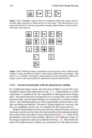
![7.10 The future of image sensing 211
Figure 7.27: Example of a “Fourier transform” photosensor for a fixed spatial
frequency. In the upper part of the chip micrograph, four photodiodes shaped
as Hanning-weighted sine and cosine functions are visible. In the lower part,
a conventional linear array of photodiodes is visible. This photosensor is the
heart of an absolute, very precise optical position encoder. Chip size is around
0.8 × 1.2 mm2 .
building blocks—electronic and photosensitive devices—with which cus-
tom functionality for a specific application can be obtained. The sym-
bolic representations of the capabilities in Fig. 7.26 are briefly summa-
rized in what follows; more details can be found in Seitz [7].
The generation of a photocurrent proportional to the incident light
is not restricted to rectangular pixel geometry as employed tradition-
ally. Applications exist wherein a suitable choice of geometry serves as
a linear or nonlinear transformation of the incident light distribution.
It is possible, for example, to “calculate” the (complex) Fourier trans-
form of a 1-D light distribution with a suitable sensor shape (see also
Section 19.4. This is illustrated in Fig. 7.27, with a photosensor opti-
mized for an absolute optical position encoder [52]: while the lower
part of the sensor is a conventional linear array of photodiodes, the
upper part consists of two harmonic photosensors in quadrature (sine
and cosine), weighted with a Hanning (cosine) window. Using such a
Fourier photosensor, the position of a 1-D periodic light pattern can
be measured with an accuracy of better than 1/1000th of the pattern
period, and the speed of such measurements easily surpasses the MHz
range.
It is even possible to make the effective shape of the photosensors
programmable, that is, electrically adaptable to changed conditions in
real-time. This is realized by adding together photogenerated charge
packets in the charge domain using the CCD principle, under control of
a digital CCD sequencer; for example, a microcontroller [53]. Spatially](https://image.slidesharecdn.com/computervision-handbookofcomputervisionandapplicationsvolume1-sensorsandimaging-120205081125-phpapp02/85/Computer-vision-handbook-of-computer-vision-and-applications-volume-1-sensors-and-imaging-236-320.jpg)
![212 7 Solid-State Image Sensing
b
a
Figure 7.28: Using the CCD principle, an image sensor with dynamic pixel
form and size can be realized: a examples of some practical pixel shapes and
sizes, emphasizing that nonuniform resolution and space-variant pixel patterns
are also possible, adaptable to a given measurement problem in real-time; b
collection of images taken with the dynamic CCD image sensor described in
Seitz et al. [53], illustrating different pixel aspect ratios and sizes.
variant pixel patterns can also be implemented, as shown by a few ex-
amples of achievable dynamic pixel patterns illustrated in Fig. 7.28a.
This property can be used to adapt the form and size of the pixels
for an optimized image data acquisition strategy, where, for example,
the resolution is chosen so that a minimum amount of image data is
acquired and processed; this is illustrated in the image collection of
Fig. 7.28b, taken with different pixel aspect ratios.
The spectral sensitivity of a detector can be changed with an elec-
trical signal, or photosensors with different spectral sensitivity can be
stacked on top of each other for a solid-state color pixel without fil-
ters. This is illustrated in Fig. 7.29 with the three quantum efficiency
curves of three overlaying p-n junctions realized with a standard CMOS
process. Shallow junctions are more sensitive to blue light, while deep
junctions are predominantly sensitive to red light. Such a simple color
sensor already has a CIE general color rendering index of RA = 70, cor-
responding to a low-quality color video camera [53].
As discussed in Section 7.4, offset currents can be added to or sub-
tracted from the photocurrents, as used for example for nonuniformity
or background cancellation. There are also several ways in which mul-
tiplication and division can be implemented. Multiplication factors can
even be made programmable using a similar voltage-storing technique
as described in Section 7.4. These capabilities are still experimental,
however, and they have not yet been developed into commercially avail-
able image sensor products.](https://image.slidesharecdn.com/computervision-handbookofcomputervisionandapplicationsvolume1-sensorsandimaging-120205081125-phpapp02/85/Computer-vision-handbook-of-computer-vision-and-applications-volume-1-sensors-and-imaging-237-320.jpg)
![7.10 The future of image sensing 213
b
1
a
c o n ta c ts
0.8
n + im p la n t
0.6
p b a s e
0.4
n - w e ll
0.2
p s u b s tra te
400 600 800 1000
Figure 7.29: Color pixels can be realized without color filters by employing
the wavelength-dependent absorption properties of silicon (Fig. 7.5): a cross
section of three overlaying p-n junctions, realized with a commercially available
CMOS process; b quantum efficiency curves of the three p-n junctions, showing
pronounced blue, green and red sensitivity. A CIE general color rendering index
of RA = 70 is achieved in practice.
Another property is that photocurrents can be redirected very quick-
ly, with sub-microsecond switching times, to different electronic cir-
cuits for further processing. An example of this capability is the real-
ization of a so-called “lock-in CCD” [54]. Each pixel of this image sen-
sor is capable of synchronously detecting the local phase, amplitude,
and offset of a 2-D temporally modulated wave field. In this way the
well-known “lock-in” detection for periodic signals can be implemented
locally within each pixel, combined with the detection of the light, as
used, for example, in optical range cameras based on the time-of-flight
principle, described for example in Section 18.5. A micrograph of such
an experimental lock-in CCD image sensor offering eight taps (sampling
values per signal period) in each pixel is shown in Fig. 7.30a. By using
more than three taps per pixel, higher-order moments or higher-order
Fourier coefficients can be determined of the modulated light. An ap-
plication of this is the discrimination of temporal code patterns for the
differentiation between various modulated light sources.
The dynamic range of optical signal detection can be increased with
a circuit or a device exhibiting nonlinear transfer characteristics, such
as the logarithmic pixel described in Section 7.3.5. As mentioned, it is of
course also possible to supply each pixel with its own amplifying circuit,
as was the original motivation for the development of APS technology.
When combined with suitable, exposure-time based multiplication and
charge summation capabilities, 2-D photocharge shifts make it possible
to realize a CCD image sensor that can acquire and convolve an optical
scene simultaneously, with a freely programmable convolution kernel
of any extent [55]. Results obtained with an experimental convolution
CCD offering 43 × 32 pixels show that the accuracy of the individual](https://image.slidesharecdn.com/computervision-handbookofcomputervisionandapplicationsvolume1-sensorsandimaging-120205081125-phpapp02/85/Computer-vision-handbook-of-computer-vision-and-applications-volume-1-sensors-and-imaging-238-320.jpg)

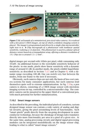
![216 7 Solid-State Image Sensing
An obvious application is the integration of all components of a
video camera on one single chip, as described, for example, in Renshaw
et al. [56]. Such single-chip video cameras are commercially available
now. Recently, an improved version of a single-chip digital camera has
been advertised, combining a 160 × 160 photodiode pixel array, auto-
exposure circuitry, all necessary analog and digital control/timing elec-
tronics, as well as an on-chip A/D converter with interface to processor-
compatible serial and parallel ports. Volume price for such a single-
chip digital camera is around $10, making it very attractive for many
practical applications such as surveillance, automatic manufacturing,
process control, picture telephony, etc. It is not difficult to imagine
that the next step can be taken as well, that is, the cointegration of
such an electronic camera with a general-purpose digital processor, ca-
pable of evaluating the acquired imagery directly on chip. Such camera-
processor products, either based on line or area cameras, are already
commercially available now [57], with the first successful industrial ap-
plications, primarily in automatic manufacturing and process control.
Consumer applications with on-chip image compression, on-chip mo-
dem for image transmission etc. have also been addressed, and it is
expected that such low-cost camera systems find applications in many
security and safety applications at home and in public places.
Various types of smart image sensors for different approaches to
range imaging have been realized. For variations of the well-established
triangulation distance-measuring technique (see Sections 18.4 and 19.4),
smart imagers exhibiting the following properties have been described:
A predefined 1-D spatial response can be obtained with suitably shaped
photosensors, exhibiting for example 1/x spatial sensitivity character-
istics, as illustrated in Fig. 7.31b. The resulting planar triangulation dis-
tance sensor achieves a distance reproducibility of around 1 % [58]. This
simple solution saves a digital processor that would have been neces-
sary for the calculation of this nonlinear transformation, and a robust,
easy-to-design single-chip distance sensor result. A 2-D array of “time-
to-maximum-light pixels” is the basis of another triangulation setup
with swept sheets of light [59]. Stereodepth vision can also be consid-
ered to be a (passive) triangulation technique (see also Section 20.2, for
which special high-speed stereodepth vision chips have been proposed,
see, for example, Hakkarainen et al. [60].
The few examples given here should serve as an indication that ma-
chine vision can profit enormously from the developments in the field
of smart image sensing. They make it possible to miniaturize, improve,
or extend known measurement techniques, while at the same time of-
ten reducing the cost and increasing the performance of the system.](https://image.slidesharecdn.com/computervision-handbookofcomputervisionandapplicationsvolume1-sensorsandimaging-120205081125-phpapp02/85/Computer-vision-handbook-of-computer-vision-and-applications-volume-1-sensors-and-imaging-241-320.jpg)
![7.10 The future of image sensing 217
7.10.3 On the way to seeing chips?
The rapid development of image sensors with more and more inte-
grated functionality led a prominent researcher in the field to proclaim
the imminence of “seeing chips” [61]. A few examples of image sen-
sors with complete, integrated image processing hardware have been
reported for certain tasks, such as the fingerprint recognition and iden-
tification chip described in Denyer et al. [57]. Various successful smart
image sensors have been demonstrated that are capable of carrying out
certain important, but still only basic functions for the vision process
on a single chip, see, for example, Koch [62]. The suspicion that “vision
is difficult” [61] has been fully verified, and it has become obvious that
the early expectations of monolithically integrated single-chip vision
systems were too high. As demonstrated for example by the finger-
print verification chip [57] it is possible today to co-integrate an image
sensor and all the necessary processing circuitry on a single chip for
the solution of a given—still not too complex—machine vision problem.
However, this would be far removed from the original idea of a seeing
chip which visually perceives some aspects of its surroundings, and in
most cases it would make no economical sense.
The basic philosophy behind the seeing chip is to distribute the pro-
cessing power over the photosensitve part. This strategy is inspired by
the biological concept of highly parallel, low-speed and low power dis-
tributed analog computing, which is the basis of nature’s marvelous
visual perceptive systems, such as our own highly-developed sense of
vision. In contrast to the planar, essentially two-dimensional semicon-
ductor fabrication technology, nature realizes fully three-dimensional
processing systems, in which each “pixel” is backed by a tremendous
number of nerve cells—more than 105 in the human visual system
[63]—performing the necessary calculation for the sense of vision. In
the near future, it will be unrealistic to expect that each pixel on a
solid-state image sensor will contain more than a few ten transistors,
while maintaining a useful pixel size of the order of 30 × 30 µm2 and
an optical fill factor of at least 10 %.
As a consequence, recent developments in the area of integrated ma-
chine vision also consider architectures based on different planes: an
image acquisition plane might be followed by several (analog) prepro-
cessing planes, an (essentially digital) classification plane and an out-
put plane, all connected using suitable high-bandwidth bus schemes
with an appropriate software protocol. This guarantees a maximum
fill factor for the image sensing part and allows for the use of optimal
architectures and technologies for the different parts of the complete
system. Such an approach does not necessarily mean that every plane
resides on its own chip; different planes can be integrated on the same
chip. The technology for stacking and interconnecting silicon chips,](https://image.slidesharecdn.com/computervision-handbookofcomputervisionandapplicationsvolume1-sensorsandimaging-120205081125-phpapp02/85/Computer-vision-handbook-of-computer-vision-and-applications-volume-1-sensors-and-imaging-242-320.jpg)
![218 7 Solid-State Image Sensing
so called 3-D or z-plane technology, has been developed [64], but the
appealing idea of a low-cost single-chip vision system, a seeing chip,
becomes seriously compromised.
The conclusion is that smart image sensors (offering additional on-
chip functionality) and integrated vision systems are certainly trends
that will lead to a wide range of practical products, albeit rarely in the
form of single, self-contained seeing chips. Instead, it can be expected
that smart image sensors with extended capabilities for the dynamic ac-
quisition of images will be part of an integrated vision system. This will
consist of an economically sensible combination of imager, analog and
digital processing parts. Special properties built into such smart image
sensors include lower noise, higher DR, programmable sensitivity, on-
chip nonuniformity and shading correction, variable exposure and tim-
ing control, region-of-interest capability, dynamic pixel size and shape,
and on-chip image preprocessing, which can be carried out for all pixels
in parallel, etc. It might well be that “seeing chip” is a misnomer, and
that the silicon retina [65], with its less exaggerated expectations and
the suggestion of more of a front-end image acquisition/pre-processing
module, is a much more appropriate name for the current and future
development directions in the field of integrated image acquisition and
processing systems.
7.11 Conclusions
It was only about a decade ago that a few researchers started to exploit
one of the most exciting capabilities offered by modern silicon-based
semiconductor technology, the monolithic integration of photosensi-
tive, analog and digital circuits. Some of the results of these efforts are
described in this work, representing just a small fraction of the many
applications already demonstrated. They all support the main asser-
tion of this chapter, that today’s image sensors are no longer restricted
to the acquisition of optical scenes. Image sensors can be supplied
with custom integrated functionality, making them key components,
application-specific for many types of optical measurement problems.
It was argued that it is not always optimal to add the desired custom
functionality in the form of highly-complex smart pixels, because an in-
crease in functionality is often coupled with a larger fraction of a pixel’s
area being used for electronic circuit, at the cost of reduced light sen-
sitivity. For this reason, each new optical measurement problem has
to be inspected carefully, taking into account technical and economical
issues. For optimum system solutions, not only smart pixels have to be
considered. Functionality could also be provided by separate on-chip
or off-chip circuits, perhaps by using commercially available electronic
components.](https://image.slidesharecdn.com/computervision-handbookofcomputervisionandapplicationsvolume1-sensorsandimaging-120205081125-phpapp02/85/Computer-vision-handbook-of-computer-vision-and-applications-volume-1-sensors-and-imaging-243-320.jpg)
![7.12 References 219
Machine vision system architects can no longer ignore the freedom
and functionality offered by smart image sensors, while being well
aware of the shortcomings of semiconductor photosensing. It may be
true that the seeing chips continue to be elusive for quite some time.
The smart photosensor toolbox for custom imagers is a reality today,
and a multitude of applications in optical metrology, machine vision,
and electronic photography can profit from the exciting developments
in this area. “Active vision,” “integrated machine vision,” “electronic
eyes,” and “artificial retinae” are quickly becoming more than concepts:
the technology for their realization is finally here now!
7.12 References
[1] Gonzalez, R. and Wintz, P., (1987). Digital Image Processing, 2nd edition.
Reading, MA: Addison-Wesley.
[2] Beck, R. (ed.), (1995). Proc. AAAS Seminar on Fundamental Issues of Imag-
ing Science, Atlanta (GA), February 16-17, 1995.
[3] Beyer, H., (1992). Geometric and radiometric analysis for a CCD-camera
based photogrammetric close-range system. PhD thesis No. ETH-9701,
Federal Institute of Technology, Zurich, Switzerland.
[4] Chamberlain, S. and Lee, J., (1984). A novel wide dynamic range silicon
photodetector and linear imaging array. IEEE Jour. Solid State Circ., SC-19:
175–182.
[5] Lenz, R., (1996). Ein Verfahren zur Schätzung der Parameter ge-
ometrischer Bildtransformationen. Dissertation, Technical University of
Munich, Munich, Germany.
[6] Schenker, P. (ed.), (1990). Conference on Active Vision, Vol. 1198 of Proc.
SPIE.
[7] Seitz, P., (1995). Smart image sensors: An emerging key technology for ad-
vanced optical measurement and microsystems. In Proc. SPIE, Vol. 2783,
pp. 244–255.
[8] Saleh, B. and Teich, M., (1991). Fundamentals of Photonics. New York:
John Wiley and Sons, Inc.
[9] Wong, H., (1996). Technology and device scaling considerations for CMOS
imagers. IEEE Trans. El. Dev., 43:2131–2142.
[10] Sze, S., (1985). Semiconductor Devices. New York: John Wiley and Sons.
[11] Spirig, T., (1997). Smart CCD/CMOS based image sensors with pro-
grammable, real-time temporal and spatial convolution capabilities for
applications in machine vision and optical metrology. PhD thesis No. ETH-
11993, Federal Institute of Technology, Zurich, Switzerland.
[12] Heath, R., (1972). Application of high-resolution solid-state detectors for
X-ray spectrometry—a review. Advan. X-Ray Anal., 15:1–35.
[13] Bertin, E., (1975). Principles and Practice of X-Ray Spectrometric Analysis.
New York: Plenum Press.
[14] Budde, W., (1979). Multidecade linearity measurements on Si photodi-
odes. Applied Optics, 18:1555–1558.](https://image.slidesharecdn.com/computervision-handbookofcomputervisionandapplicationsvolume1-sensorsandimaging-120205081125-phpapp02/85/Computer-vision-handbook-of-computer-vision-and-applications-volume-1-sensors-and-imaging-244-320.jpg)
![220 7 Solid-State Image Sensing
[15] Theuwissen, A., (1995). Solid-State Imaging with Charge-Coupled Devices.
Dordrecht, The Netherlands: Kluwer Academic Publishers.
[16] Vietze, O. and Seitz, P., (1996). Image sensing with programmable offset
pixels for increased dynamic range of more than 150 dB. In Conference
on Solid State Sensor Arrays and CCD Cameras, Jan. 28–Feb. 2, 1996, San
Jose, CA, Vol. 2654A, pp. 93–98.
[17] Vietze, O., (1997). Active pixel image sensors with application specific
performance based on standard silicon CMOS processes. PhD thesis No.
ETH-12038, Federal Institute of Technology, Zurich, Switzerland.
[18] Webb, P., McIntyre, R., and Conradi, J., (1974). Properties of Avalanche
Photodiodes. RCA Review, 35:234–277.
[19] Seitz, P., (1997). Image sensing with maximum sensitivity using industrial
CMOS technology. In Conference on Micro-Optical Technologies for Mea-
surement Sensors and Microsystems II, June 16–June 20, 1997, Munich,
Germany, Vol. 3099, pp. 22–33.
[20] Zappa, F., Lacatia, A., Cova, S., and Lovati, P., (1996). Solid-state single-
photon detectors. Optical Engineering, 35:938–945.
[21] Mathewson, A., (1995). Integrated avalanche photo diode arrays. Ph.D.
thesis, National Microelectronics Research Centre, University College,
Cork, Ireland.
[22] Mahowald, M., (1991). Silicon retina with adaptive photodetectors. In
Conference on Visual Information Processing: From Neurons to Chips Jan.
4, 1991, Orlando, FL, Vol. 1473, pp. 52–58.
[23] Graf, H., Höfflinger, B., Seger, Z., and Siggelkow, A., (1995). Elektronisch
Sehen. Elektronik, 3:3–7.
[24] Sankaranarayanan, L., Hoekstra, W., Heldens, L., and Kokshoorn, A.,
(1991). 1 GHz CCD transient detector. In International Electron Devices
Meeting 1991, Vol. 37, pp. 179–182.
[25] Colbeth, R. and LaRue, R., (1993). A CCD frequency prescaler for broad-
band applications. IEEE J. Solid-State Circ., 28:922–930.
[26] Carnes, J. and Kosonocky, W., (1972). Noise sources in charge-coupled
devices. RCA Review, 33:327–343.
[27] Allen, P. and Holberg, D., (1987). CMOS Analog Circuit Design. Fort Worth:
Saunders College Publishing.
[28] Hopkinson, G. and Lumb, H., (1982). Noise reduction techniques for CCD
image sensors. J. Phys. E: Sci. Instrum, 15:1214–1222.
[29] Knop, K. and Seitz, P., (1996). Image Sensors. In Sensors Update, W. G.
Baltes, H. and J. Hesse, eds., pp. 85–103. Weinheim, Germany: VCH-
Verlagsgesellschaft.
[30] Chandler, C., Bredthauer, R., Janesick, J., Westphal, J., and Gunn, J., (1990).
Sub-electron noise charge coupled devices. In Conference on Charge-
Coupled Devices and Solid State Optical Sensors, Feb. 12–Feb. 14, 1990,
Santa Clara, CA, Vol. 1242, pp. 238–251.
[31] Janesick, J., Elliott, T., Dingizian, A., Bredthauer, R., Chandler, C., West-
phal, J., and Gunn, J., (1990). New advancements in charge-coupled device
technology. Sub-electron noise and 4096 X 4096 pixel CCDs. In Confer-](https://image.slidesharecdn.com/computervision-handbookofcomputervisionandapplicationsvolume1-sensorsandimaging-120205081125-phpapp02/85/Computer-vision-handbook-of-computer-vision-and-applications-volume-1-sensors-and-imaging-245-320.jpg)
![7.12 References 221
ence on Charge-Coupled Devices and Solid State Optical Sensors, Feb. 12–
Feb. 14, 1990, Santa Clara, CA, Vol. 1242, pp. 223–237.
[32] Matsunaga, Y., Yamashita, H., and Ohsawa, S., (1991). A highly sensitive
on-chip charge detector for CCD area image sensor. IEEE J. Solid State
Circ., 26:652–656.
[33] Fossum, E., (1993). Active pixel sensors (APS)—are CCDs dinosaurs? In
Conference on Charge-Coupled Devices and Solid-State Optical Sensors III,
Jan. 31–Feb. 2, 1993, San Jose, CA, Vol. 1900, pp. 2–14.
[34] Mendis, S., Kemeny, S., Gee, R., Pain, B., Staller, C., Kim, Q., and Fossum, E.,
(1997). CMOS active pixel image sensors for highly integrated imaging
systems. IEEE J. Solid-State Circ., 32:187–197.
[35] Pratt, W., (1991). Digital Image Processing, 2nd edition. New York: Wiley.
[36] Benson, K., (1986). Television Engineering Handbook. New York: McGraw
Hill.
[37] Ramo, S., Whinnery, J. R., and van Duzer, T., (1994). Fields and waves in
communication electronics, 3rd edition. New York: Wiley.
[38] Jackson, J. D., (1975). Classical Electrodynamics, 2nd edition. New York:
Wiley.
[39] Gagnaire, M., (1997). An overview of broad-band access technologies.
Proc. IEEE, 85:1958–1972.
[40] Pritchard, D. H., (1984). U.S. color television fundamentals — a review.
RCA Engineer, 29:15–26.
[41] Hunt, R. W. G., (1991). Measuring Colour, 2nd edition. Ellis Horwood.
[42] Bayer, B. E., (1976). Color imaging array, U.S. patent No. 3,971,065.
[43] Knop, K., (1985). Two-dimensional color encoding patterns for use in
single chip cameras. Proc. SPIE, 594:283–286.
[44] Aschwanden, F., Gale, M. T., Kieffer, P., and Knop, K., (1985). Single-chip
color camera using a frame-transfer CCD. IEEE Trans. Electron. Devices,
ED-32:1396–1401.
[45] Arnold, L., (1992). Moderne Bildkomminikation. Heidelberg: Hüthig Ver-
lag.
[46] Davis, A. W., (1997). Where the cameras will fit in. Advanced Imaging,
Nov. 97:43–49.
[47] Kreider, G., Bosiers, J., Dillen, B., van der Heijden, J., Hoekstra, W., Klein-
mann, A., Opmeer, P., Oppers, J., Peek, H., Pellens, R., and Theuwissen, A.,
(1995). An mK × mK Modular Image Sensor Design. In International Elec-
tron Devices Meeting 1995, Washington, D. C., pp. 155–158.
[48] Peek, H. L., Verbugt, D. W., Beenhakkers, M. J., Huininck, W. F., and
Kleimann, A. C., (1996). An FT-CCD imager with true 2.4 × 2.4 µm2 pix-
els in double mebrane poly-Si technology. In Proceedings of the IEDM ’
96, International Electron Devices Meeting, San Francisco, Dec.. 8-Dec. 11,
1996, pp. 907–910.
[49] MOSIS, (1999). MOSIS VLSI fabrication service, Information Sciences Insti-
tute, University of Southern California, USA, Marina del Rey, CA 90292-
6695; http://www.mosis.org/.](https://image.slidesharecdn.com/computervision-handbookofcomputervisionandapplicationsvolume1-sensorsandimaging-120205081125-phpapp02/85/Computer-vision-handbook-of-computer-vision-and-applications-volume-1-sensors-and-imaging-246-320.jpg)
![222 7 Solid-State Image Sensing
[50] Flores, J., (1992). An analytical depletion-mode MOSFET model for analy-
sis of CCD output characteristics. In Conference on High-Resolution Sen-
sors and Hybrid Systems, Feb. 9–Feb. 14, 1992, San Jose, CA, Vol. 1656,
pp. 466–475.
[51] Raynor, J. and Seitz, P., (1997). A linear array of photodetectors with
wide dynamic range and near photon quantum noise limit. Sensors and
Actuators A, 61:327–330.
[52] Engelhardt, K. and Seitz, P., (1996). Absolute, high-resolution optical po-
sition encoder. Applied Opics, 35:201–208.
[53] Seitz, P., Leipold, D., Kramer, J., and Raynor, J. M., (1993). Smart optical
and image sensors fabricated with industrial CMOS/CCD semiconductor
processes. Proc. SPIE, 1900:21–30.
[54] Spirig, T., Seitz, P., Vietze, O., and Heitger, F., (1995). The lock-in CCD.
Two-dimensional synchronous detection of light. IEEE J. Quantum Elec-
tronics, 31:1705–1708.
[55] Spirig, T., Seitz, P., Vietze, O., and Heitger, F., (1997). A smart CCD im-
age sensor with real-time programmable parallel convolution capabilities.
IEEE Trans. Circuits and Systems, 44:465–468.
[56] Renshaw, D., Denyer, P., Wang, G., and Lu, M., (1990). ASIC vision. In Proc.
of the IEEE 1990 Custom Integrated Circuits Conference, Feb. 14–Feb. 16,
1990, Dan Francisco, CA, pp. 7.3.1–7.3.4.
[57] Denyer, P., Renshaw, D., and Smith, S., (1995). Intelligent CMOS imaging.
In Conference on Charge-Coupled Devices and Solid-State Optical Sensors
V, Feb. 5–Feb. 10, 1995, San Jose, CA, Vol. 2415, pp. 285–291.
[58] Kramer, J., Seitz, P., and Baltes, H., (1994). Planar distance and velocity
sensor. IEEE Jour. Quantum Electronics, 30:2726–2730.
[59] Gruss, A., Carley, L., and Kanade, T., (1991). Integrated sensor and range-
finding analog signal processor. IEEE J. Solid State Circ., 26:184–192.
[60] Hakkarainen, J., Little, J., Lee, H., and Wyatt, J., (1991). Interaction of al-
gorithm and implementation for analog VLSI stereo vision. In Conference
on Visual Information Processing: From Neurons to Chips, Jan. 4, 1991,
Orlando, FL, Vol. 1473, pp. 173–184.
[61] Koch, C., (1989). Seeing chips: analog VLSI circuits for computer vision.
Neural Computation, 1:184–200.
[62] Koch, C., (1991). Implementing early vision algorithms in analog
hardware—an overview. In Conference on Visual Information Processing:
From Neurons to Chips, Jan. 4, 1991, Orlando, FL, Vol. 1473, pp. 2–15.
[63] Hubel, D., (1988). Eye, Brain and Vision. New York: Scientific American
Library.
[64] Carson, J. (ed.), (1989). Materials, devices, techniques and applications for
Z-plane focal plane array technology, Vol. 1097 of Proc. SPIE.
[65] Mahowald, M. and Mead, C., (1991). The silicon retina. Scientific American,
264:40–46.](https://image.slidesharecdn.com/computervision-handbookofcomputervisionandapplicationsvolume1-sensorsandimaging-120205081125-phpapp02/85/Computer-vision-handbook-of-computer-vision-and-applications-volume-1-sensors-and-imaging-247-320.jpg)

![224 8 HDRC-Imagers for Natural Visual Perception
For Michelangelo or Rembrandt, their wish was to preserve the beauty
of a moment, a person, or a landscape by creating an image that would
last forever.
The development of photography in the last two centuries allowed a
huge advance in that area and today still represents the state of the art
in imaging. So far, no electronic system comes close to the photography
standard and even the best film materials fall short in situations where
the dynamic range is very high.
8.2 Log compression at the pixel site
In the late 1960s and early 1970s Tomita [1] and Cornsweet [2] showed
that the responsivity of cone receptors has a logarithmic characteris-
tic. Eye-like logarithmic compression overcomes most of the dynamic
range-related restrictions. Different approaches of log compression
have been examined [3] but technological variability of critical param-
eters foiled the manufacture of large area sensors. Advances in MOS
technology and circuit concepts as well as new system structures allow
these problems to be overcome today.
To understand the advantage of log signal compression, it is nec-
essary to take a close look at what the signal or information is. The
information in images is (with only a few exceptions) the contrast [4,
5]. Intensities in most images, with the possible exception of light
sources themselves, are the product of irradiation and the reflectiv-
ity/absorptivity of imaged objects as well as the absorptivity of the
medium that is in between the light source, the object and the imager.
In situations where scattering and light transmission effects can be ne-
glected, the intensities within an image are the product of the irradiance
E and the reflectance ρ of the imaged surface.
Technical surfaces show reflectance values between 5 % (black sur-
face, nearly absorbing all light energy) and 95 % (bright shining sur-
face nearly reflecting all light energy seen at a short distance). So far
a dynamic range of 20 : 1 is necessary for all the variations within
this scenery to have a signal-to-noise ratio (SNR) of at least one. High-
dynamic range requirements arise from higher SNR demands and are
caused by varying illumination. In fact, illumination can vary not only
by factors of tens of thousands between moonlight and bright sunshine
but also between a bright headlamp and shadowed regions by night and
even between bright direct reflections of the sun and shadowed regions
under daylight conditions. With technical light sources, apertures and
optical filters, it is also possible to generate illumination variations in
a scene that span several decades.
The response S of a linear converting device is S ≈ Eρ. With a
(HDRC) sensor the response will be S ≈ log E + log ρ. Two different](https://image.slidesharecdn.com/computervision-handbookofcomputervisionandapplicationsvolume1-sensorsandimaging-120205081125-phpapp02/85/Computer-vision-handbook-of-computer-vision-and-applications-volume-1-sensors-and-imaging-249-320.jpg)


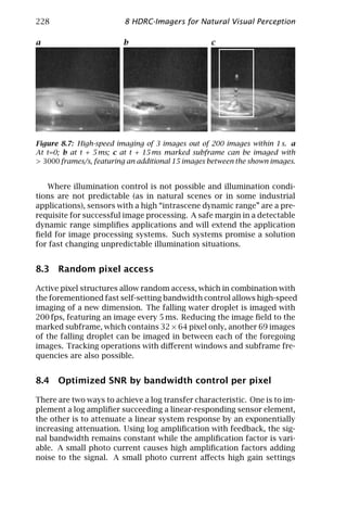
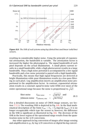
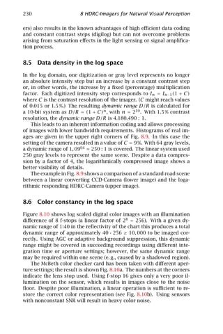

![232 8 HDRC-Imagers for Natural Visual Perception
a b
Figure 8.10: a Log image of McBeth chart with f-stops as indicated; b same as
a but normalized to black and white for each quarter; (see also Plate 1).
Figure 8.11: Noiseless McBeth chart generated synthetically for comparison
with Fig. 8.10; (see also Plate 2).
the one hand, the continuous shrinking of structure dimensions in
modern CMOS processes supports this endeavor. On the other hand,
the improvement of performance criteria of large HDRC sensor arrays
(such as readout speed or homogeneity) requires a certain amount of
circuitry footprint in each pixel. To retain a fill factor of about 40 %, a
percentage sufficient for avoidance of aliasing effects in the image, the
pixel size has a lower limit, which is a factor 35 up to 40 above the min-
imum feature size of the used CMOS process. On the other hand, total
chip size is bound by lithography exposure fields and process yield to
a chip diagonal of 25 mm [6]. As can be seen in Fig. 8.12, an HDRC
sensor with VGA resolution can be fabricated with an economic chip
with a diagonal below 10 mm.
The chip diagonal influences the system costs directly, especially
as regards chip and optics prices together. Reflections and scatter-
ing within the optics have to be minimized because even low intensity
ghosts (and reflections) will appear in the image. Further improvement
of the effective fill factor can be achieved with microlens arrays.
The HDRC sensors benefit from the evolution of structure sizes in
CMOS technology as well as from the increasing number of metalliza-](https://image.slidesharecdn.com/computervision-handbookofcomputervisionandapplicationsvolume1-sensorsandimaging-120205081125-phpapp02/85/Computer-vision-handbook-of-computer-vision-and-applications-volume-1-sensors-and-imaging-257-320.jpg)
![8.7 Development of functionality and spatial resolution 233
1,4
act. HDRC development
minimum lithographic feature size [µm] 1,2 128x256
256x384
256x512
1 480x640
0,8
0,6
700x1000 array size
with optimized pixel
0,4
0,2
0 5 10 15 20 25
Image field diagonal [mm]
Figure 8.12: Development of imager diagonals with decreasing feature sizes.
tion layers and the high level of planarization available on recent tech-
nology generations. The active transistor channel area even in pixels
with complex architectures covers a fraction of only 3-5 % of the pixel
cell, a value that has been constant over several technology generations.
The major area (about 50 %) is required for diffusion separations, well
contacts, and other interconnects.
Mostly induced by local variations of semiconductor process param-
eters such as interface state densities, solid-state imagers suffer from
so-called fixed-pattern noise (FPN). The HDRC sensors with their pixel-
internal lin-log conversion exhibit this phenomenon as a pure offset
overlay on the image that can be corrected in real-time at the video sig-
nal output. The video pad buffers of recently developed HDRC imagers
provide an offset cancellation feature that operates on the analog sig-
nal path. The correction pattern requests a memory size of 1 byte per
pixel to yield a resolution of 500 µV. On-chip D/A conversion and the
FPN cancellation on the analog signal path provides a proper adjust-
ment of the operation input range of the external video A/D converter
and saves system cost. Image overlay information for the correction of
fixed pattern noise is constant over the lifetime of the sensor and can
be stored permanently in the system.
As the purpose of acquired images is shifted more and more from
documentation and communication towards the control input of au-
tonomous systems, low-level image processing operations are best per-
formed shortly afterwards or at sensor level. Spatial filtering for noise
reduction purposes or edge enhancement for image segmentation are
the most time-consuming tasks on digital image processing systems.](https://image.slidesharecdn.com/computervision-handbookofcomputervisionandapplicationsvolume1-sensorsandimaging-120205081125-phpapp02/85/Computer-vision-handbook-of-computer-vision-and-applications-volume-1-sensors-and-imaging-258-320.jpg)
![234 8 HDRC-Imagers for Natural Visual Perception
Resistive grids operating with analog voltages to adapt the functions
of biological systems have been placed on the sensor chip to implement
the forementioned low-level operations. This approach provides mas-
sive parallel processing in real-time with moderate effort by hardware.
In the examples of focal plane image processing described by Mead and
Mahowald [7], the individual photodiodes are directly connected to the
input nodes of the resistive grid. The signal bandwidth at the output
of these so-called early-vision systems is drastically reduced, allowing
compact system design.
However, it is also obvious that imager performance will be down-
graded as a result of integrating these additional functions. On the
one hand, pixel size and fill factor will be restricted as well, the high
demand for power that results from such a high number of elements
also has to be taken into account. Moreover, incident light influences
the proper function of analog circuits, which finally limits use of these
approaches.
Technology progress in the digital domain and continuously grow-
ing processing power of dedicated digital image processors and the
independent development cycles of hardware and software are the win-
ning points of pure digital image processing.
The following approach, however, shows a combination of massive
parallel analog processing and serialized image data communication.
The “retina chip” [8], which mimics the function of the already proven
retina chip from Mahowald was developed for real-time post-processing
HDRC images. The purpose of this device is to level the gray-scale varia-
tions that occur over larger distances in the image while simultaneously
enhancing the image.
The complexity of a single cell of about 60 transistors occupying
an area of 66 × 100 µm2 shows clearly the mismatch to imager chips.
Implementing the retina chip as a stand-alone post-processor offers the
opportunity to choose an array size with fewer rows than the imager’s
vertical extension.
As a result of the short settling time of the net after loading a row
of image data and the limited affected area, a small grid can be used
repetitively during processing a complete image. Presuming an ade-
quate organization of load and read addresses in the retina, a net as
wide as the imager and 32 rows in height is sufficient for full image
processing.
The advantages over existing focal plane solutions are: the possi-
bility of gaining the original image data from the imager itself and of
being able to process data from different processing levels separately;
only 1/10th of the retinal cells need to be used in the focal plane ap-
proach; the superb fill factor reached in the sensor part; the possibility
of correcting for imager nonuniformity before post-processing image](https://image.slidesharecdn.com/computervision-handbookofcomputervisionandapplicationsvolume1-sensorsandimaging-120205081125-phpapp02/85/Computer-vision-handbook-of-computer-vision-and-applications-volume-1-sensors-and-imaging-259-320.jpg)
![8.8 References 235
data; and the independence of development cycles and technologies
for imager and retina device.
The HDRC (High-Dynamic Range CMOS) is a registered trademark
of Institute for Microelectronics, Stuttgart, Germany. The HDRC-Tech-
nology as well as the functional principle of logarithmic sensor cells
implementing weak inversion transistors for achieving the log response
are patented by the Institute for Microelectronics, Stuttgart.
8.8 References
[1] Tomita, T., (1968). Electrical response of single photo receptors. Proc. IEEE
(Special Issue on Neural Studies), 56:1015–1023.
[2] Cornsweet, T. N., (1970). Visual Perception. New York: Academic Press.
[3] Chamberlain, S. and Lee, J. P. Y., (1984). A novel wide dynamic range silicon
photodetector and linear imaging array. IEEE Journal of Solid State Circuits,
SC-19(1):41–48.
[4] Boring, C. G., (1950). A History of Experimental Psychology. New York:
Appleton-Century-Crofts.
[5] Hurvich, L. M. and Jameson, D., (1966). The perception of Brightness and
Darkness. Boston: Allyn and Bacon.
[6] Wong, H. S., (1996). Technology and Device Scaling Considerations for
CMOS Imagers. IEEE Trans. ED, 43(12):2131–2142.
[7] Mead, C. A. and Mahowald, M. A., (1988). Silicon Model of Early Visual
Processing. Neural Networks, 1:91–97.
[8] Apel, U., Graf, H. G., Höfflinger, B., Regensburger, U., and Seger, U., (1998).
Continuous parallel analogue image processing using time discrete sam-
pling. In Advanced Microsystems for Automotive Applications, E. Ricken
and W. Gessner, eds., pp. 149–156. Berlin: Springer.](https://image.slidesharecdn.com/computervision-handbookofcomputervisionandapplicationsvolume1-sensorsandimaging-120205081125-phpapp02/85/Computer-vision-handbook-of-computer-vision-and-applications-volume-1-sensors-and-imaging-260-320.jpg)


![238 9 Image Sensors in TFA (Thin Film on ASIC) Technology
b
a
Optical detector
Front electrode
a-Si:H thin film system
Rear electrode
Insulation layer
ASIC
Figure 9.1: a Schematic layer sequence of a TFA image sensor; b process
chambers of a Plasma Enhanced Chemical Vapor Deposition (PECVD) ultrahigh-
vacuum cluster system.
9.1 Introduction
As computer vision systems become more ambitious, the performance
of image sensors has become especially important. Future image sen-
sors are expected not only to provide raw signals, but also to include
part of the image processing system on-chip. This approach is suited to
lower fabrication costs and improvement of sensor performance. Due
to their inflexible function principle and technology, commonly used
charge-coupled devices (CCDs) suffer from several disadvantages with
regard to dynamic range, fill factor and feasibility of on-chip electron-
ics [1]. Lately, CMOS imagers have become competitive by overcoming
some of these drawbacks by using CMOS circuitry and a photodiode or
photogate employing the same technology as the optical detector [2].
Unlike a CMOS imager, a sensor in Thin Film on ASIC (TFA) tech-
nology is vertically integrated, providing a fill factor close to 100 % for
both the detector and the circuitry. Another benefit of TFA is flexi-
bility because the technology allows separate design and optimization
of either component. An existing ASIC can be supplied with different
detector structures for application-specific device optimization. The
basic structure of a TFA sensor is depicted in Fig. 9.1a. The detector
is formed by an a-Si:H thin-film system that is sandwiched between a
metal rear electrode and a transparent front electrode [3, 4]. The crys-
talline ASIC typically includes identical pixel circuitry underneath each
pixel detector and peripheral circuitry outside the light-sensitive area.
This chapter provides a survey of TFA research results to date and
outlines future TFA applications and solutions. In Section 9.2, differ-
ent thin-film detector structures are studied with regard to spectral
sensitivity, dark current, temperature behavior and long-term stabil-
ity. The combination of thin-film detector and ASIC is evaluated in](https://image.slidesharecdn.com/computervision-handbookofcomputervisionandapplicationsvolume1-sensorsandimaging-120205081125-phpapp02/85/Computer-vision-handbook-of-computer-vision-and-applications-volume-1-sensors-and-imaging-263-320.jpg)


![9.2 Thin-film detectors 241
Figure 9.3: Relative spectral response of a pin photodiode for moderate reverse
bias (-1 V).
However, light soaking experiments with the optimized pin photodetec-
tors revealed almost stable device characteristics under realistic illumi-
nation conditions. After daylight exposure (100,000 lx) for an illumina-
tion period of 16 h, virtually no variation of the dark and photocurrent
was found within the experimental accuracy [5]. One reason for the ex-
cellent long-term stability of pin photodetectors is that they are always
operated under zero or reverse bias, while the Staebler-Wronsky effect
is associated with carrier injection.
Due to the bandgap of amorphous silicon the spectral sensitivity of
a-Si:H devices matches the responsivity of the human eye that peaks in
the green spectral range. This behavior is verified by the spectral re-
sponse shown in Fig. 9.3 under slightly negative bias voltage (-1 V). The
response curve exhibits a maximum for 580 nm close to the green spec-
tral region. The absolute response values for the test structures are lim-
ited to about 0.1 AW-1 due to the poor transparency of the Al front con-
tact. However, by application of a transparent conductive oxide (TCO)
with considerably higher transparency, the quantum efficiency can be
increased to more than 90 %. As the photocurrent of the pin device
approaches nearly the saturation value even under short-circuit condi-
tions, there is only a slight increase of the response curves for rising
negative bias voltages.
Because in many sensor applications readout speed is a very impor-
tant parameter, the transient behavior of the photodetector is of funda-
mental interest. The photocurrent rise and decay after switching on and
off illumination of a pin diode is demonstrated in Fig. 9.4a,b. Illumina-
tion is performed with a pulsed light-emitting diode (LED) (pulsewidth:
80 ms) with a broad spectral distribution around 565 nm, approximat-
ing a 1000 lx light exposure. The experimental results reveal that steady-
state conditions are reached within a few microseconds after switching
on illumination irrespective of the incident illumination level. A slight](https://image.slidesharecdn.com/computervision-handbookofcomputervisionandapplicationsvolume1-sensorsandimaging-120205081125-phpapp02/85/Computer-vision-handbook-of-computer-vision-and-applications-volume-1-sensors-and-imaging-266-320.jpg)
![242 9 Image Sensors in TFA (Thin Film on ASIC) Technology
a b
Figure 9.4: Photocurrent transients of a pin photodiode after: a switching on;
and b off illumination for different illumination levels at a bias voltage of −1.5 V.
increase of the photocurrent after this time range is caused by trapping
of carriers that occurs after the illumination pulse. In contrast to the
very fast photocurrent rise the decay after switching off illumination
exhibits a more complicated behavior. After an initial reduction of the
current within 10 µs a quasi-stationary plateau occurs during which the
transient current decreases only slowly. In the millisecond range the
decay exhibits a steeper decrease. The significant intermediate plateau
is attributed to thermal emission of trapped carriers into the extended
states and subsequent field-assisted extraction and is directly linked to
the continuous density of states within the bandgap. Carriers trapped
in shallow states are emitted much faster than deeply trapped ones.
This effect is responsible for the observed behavior that tends to in-
crease decay times for decreasing illumination intensity.
Another type of b/w detector makes use of a metal-semiconductor
contact (Schottky contact). This approach employs a semitransparent
metal with high work function (e. g., Pd) or a transparent conductive
contact (ITO) on top of an intrinsic a-Si:H layer. The steady-state as
well as the transient experimental results of Schottky diodes are quite
similar to those for the pin diode shown in the foregoing [6, 7].
9.2.3 Thin-film detector structures for color recognition
Besides simple b/w detection amorphous silicon multilayers have also
capabilities in color recognition. In the past, a variety of two termi-
nal color devices have been developed mainly based on a back-to-back
diode configuration (nipin, pinip and related device structures) [8, 9,
10, 11, 12]. Common to all of these color detectors is that they ex-](https://image.slidesharecdn.com/computervision-handbookofcomputervisionandapplicationsvolume1-sensorsandimaging-120205081125-phpapp02/85/Computer-vision-handbook-of-computer-vision-and-applications-volume-1-sensors-and-imaging-267-320.jpg)

![244 9 Image Sensors in TFA (Thin Film on ASIC) Technology
a
b
Figure 9.5: Deposition scheme and schematic electric field profile within: a a
nipi2 n; and b a pi3 n multilayer.
For positive bias the top diode is reverse-biased and carriers generated
by blue light illumination are extracted.
With a high color separation between red and green as the most
important goal of device optimization the drift parameters in the two
i-layers of the bottom diode have to be adjusted as different as possi-
ble while the higher drift length is required in the first i-layer. Because
the difference in the dielectric constants is not sufficient, additional
µτ-engineering is desired. For enhancement of the µτ-product of the
a-SiC:H material these layers have been deposited under strong hydro-
gen dilution of the silane/methane source gas mixture. This has been
proven to be necessary because the µτ-product of amorphous silicon
carbon alloys deposited solely from silane and methane is about a fac-
tor of five smaller than in pure a-Si:H. In contrast, the hydrogen-diluted
a-SiC:H films exhibit carrier transport parameters that are one order of
magnitude better than films with equivalent bandgap deposited with-
out hydrogen dilution as has been verified by photoconductivity mea-
surements on single layers deposited at nominally the same deposition
parameters. Another approach to improve the electric field distribu-
tion within the bottom diode employs a superthin n-layer between the
a-SiC:H and the a-Si:H region that leads to a nipi(δn)in structure [13].
The spectral response curves as a function of bias voltage for an
optimized nipi2 n multilayer are given in Fig. 9.6a. The data demon-
strate blue response for positive applied bias with a peak wavelength
of 480 nm while a shift of sensitivity is found in the negative bias range.
Down to -0.6 V the sensor is sensitive to green (550 nm) and for de-
creasing the negative bias below -1.0 V the peak wavelength turns to
red (620 nm) along with a significant increase of sensitivity until satu-](https://image.slidesharecdn.com/computervision-handbookofcomputervisionandapplicationsvolume1-sensorsandimaging-120205081125-phpapp02/85/Computer-vision-handbook-of-computer-vision-and-applications-volume-1-sensors-and-imaging-269-320.jpg)

![246 9 Image Sensors in TFA (Thin Film on ASIC) Technology
range. This behavior is supported by the thin i-layer of the top diode
(80 nm) and has also been observed for nipin two color detectors [13].
One of the most severe drawbacks common to all color detectors
with bipolar operation, including the forementioned nipi2 n color detec-
tor, is the transient behavior that suffers from long-term trap recharg-
ing currents caused by the back-to-back configuration of two diodes.
The transients after changes of bias or illumination show a signifi-
cant dependence of the illumination level, and steady-state condition
is reached later the lower the illumination intensity. This disadvanta-
geous transient behavior has been observed for nipin two color detec-
tors [14, 15] as well as for nipi2 n three color devices [16].
The speed limitations for color detectors based on antiserial diode
structures are overcome by unipolar devices explained in the following.
This type of color detector is based on a simple pin or nip structure with
the intrinsic absorber subdivided into two or more i-layers by abruptly
or continuously changing the source gas mixture during deposition, re-
sulting in pi3 n or ni2 p layer sequences, for instance. These multilayers
contain at least one heterojunction that causes different collection pa-
rameters in the adjacent i-layers in analogy to the bottom diode of the
nipi2 n structure discussed in the foregoing. In an optimized three color
detector the bandgap as well as the µτ-product decrease in the i-layers
when passing through the device in light penetration direction. Due to
the dielectric constant that is correlated with the bandgap, the electric
field drops from the top to the bottom i-layer as sketched in Fig. 9.5b.
The electric field profile in conjunction with the generation profile al-
lows collection of carriers generated by strongly absorbed radiation for
low values of reverse bias or in short-circuit conditions. With increas-
ing reverse bias the collection of carriers from deeper regions in the
device is enhanced, resulting in a red shift of the spectral sensitivity.
The main advantage of unipolar color diodes with respect to the bipo-
lar ones consists in the operation mode that ensures that the device
is permanently operated in reverse bias direction, thus avoiding time-
consuming trap recharging effects occurring in forward-biased diodes.
Furthermore, the bias voltages of unipolar detectors are in the same
range as usual ASIC supply voltages.
Figure 9.6b demonstrates the voltage-controlled variation of the spec-
tral response of a ni2 p two color detector consisting of a wide bandgap
(135 nm) a-SiC:H i-layer in front of a normal bandgap (1000 nm) a-Si:H
layer sandwiched between a top n- and bottom p-layer providing the
built-in electric field. The maximum of the response curves shifts con-
tinuously from 490 nm for short circuit to 620 nm for 1 V reverse bias
while the absolute sensitivity increases as well. It becomes obvious that
the response curves measured for higher value of reverse bias always
include the curves obtained for lower bias, thus indicating that carrier
collection proceeds towards deeper regions for increasing reverse bias.](https://image.slidesharecdn.com/computervision-handbookofcomputervisionandapplicationsvolume1-sensorsandimaging-120205081125-phpapp02/85/Computer-vision-handbook-of-computer-vision-and-applications-volume-1-sensors-and-imaging-271-320.jpg)
![9.2 Thin-film detectors 247
Figure 9.8: I/V characteristics of a ni2 p two color detector in the dark and under
various monochromatic illumination levels.
This effect is responsible for the less pronounced color separation of
unipolar photodiodes in comparison to bipolar color detectors.
The unipolar a-SiC:H/a-Si:H color detectors exhibit outstanding dy-
namic range of more than 120 dB (Fig. 9.7b) due to an extremely low
dark current around 3 × 10⁻¹¹ A cm−2 that is nearly independent of bias
voltage for reverse bias up to 3 V. The mentioned value is close to the
limit of the thermal generation current for the i-layer given by Street
[17] so that the absence of contact injection and local shunt effects can
be concluded. The photocurrent shows a slight increase in the voltage
range between short circuit and 1 V reverse bias correlating with the
onset of red sensitivity and perfect saturation for higher amounts of
reverse bias.
In order to get an impression of linearity in Fig. 9.8 the I/V character-
istics of the ni2 p detector are plotted for blue (450 nm) and red (620 nm)
monochromatic illumination conditions at various illumination levels
(ranging from 1010 - 1015 photons cm−2 s−1 ). The currents exhibit exact
linearity with regard to the illumination level. The measured values jph
obey the commonly found photoconductivity relation
jph ∝ Φγ (9.1)
while the exponent γ is almost identical to one. Furthermore, the
I/V curves demonstrate an interesting feature concerning the blue/red
color separation. The crossing points between the blue and red illu-
mination curves show a remarkable shift to open-circuit conditions by
about 0.12 V per decade for decreasing illumination intensity. This ef-
fect is caused mainly by free and trapped carriers that have major influ-](https://image.slidesharecdn.com/computervision-handbookofcomputervisionandapplicationsvolume1-sensorsandimaging-120205081125-phpapp02/85/Computer-vision-handbook-of-computer-vision-and-applications-volume-1-sensors-and-imaging-272-320.jpg)
![248 9 Image Sensors in TFA (Thin Film on ASIC) Technology
a b
Figure 9.9: Photocurrent transients of a ni2 p two color detector photodiode after
switching a from 0 V to -1 V; and b from -1 V to 0 V for different illumination
levels.
ence on the electric field profile for higher generation rates. A similar
trend has been found for other device structures by numerical sim-
ulations [18]. This result clearly indicates that not only the physical
absorption and transport parameters of the intrinsic layers determine
the device functionality, but also the charge carriers generated during
operation. As a consequence, the applicable illumination range of the
device is limited to a value smaller than the dynamic range mentioned
in the foregoing when full color recognition is required.
The most important advantage of the unipolar color detectors over
the bipolar ones is the superior transient behavior. Due to the simpler
device geometry and the operation principle, the unipolar detectors
never need to be operated in forward bias, resulting in faster current
transients. Figure 9.9 displays the transient photocurrent measured
after switching of bias between the two operation voltages for the sam-
ple illuminated with white light of variable intensity. The two switch-
ing transients show significant differences. For the reverse-bias pulse
(0 V → 1 V, blue to red sensitivity) after an initial capacitive peak the
steady-state current is reached within a 10 % tolerance interval after
about 600 µs independent of the illumination level. However, if switch-
ing is performed from reverse bias into short-circuit conditions (red to
blue sensitivity) a different behavior can be noticed. Here the current
transients show a remarkable illumination dependence that manifests
in a longer delay before the steady state is reached for lower light in-
tensity. The measured time required for recharging the traps ranges
from 200 µs for 10,000 lx to 5 ms for 100 lx. Moreover, the peaks in
the logarithmic current scale indicate a change in the direction of the](https://image.slidesharecdn.com/computervision-handbookofcomputervisionandapplicationsvolume1-sensorsandimaging-120205081125-phpapp02/85/Computer-vision-handbook-of-computer-vision-and-applications-volume-1-sensors-and-imaging-273-320.jpg)
![9.3 TFA properties and design considerations 249
photocurrent during the transient. Partial field reversal in the bottom
i-layer and injection of holes from the rear p-layer are assumed to be
responsible for the current flowing opposite to the steady-state value
during the transient until the charge state of the traps has rearranged.
The observed effect is coupled to the low-field region in the bottom i-
layer and seems to be inherent to devices containing regions with low
electric field. To much less extent the same tendency can also be found
for simple pin diodes. With regard to application of the color detector
in two-dimensional image sensor arrays the prolonged duration of the
transient current that occurs only for one switching process does not
define a general drawback. For example, this delay time can be used
for readout of the color sensor array that takes several milliseconds
depending on the dimensions of the sensor matrix.
9.3 TFA properties and design considerations
9.3.1 Noise in TFA sensors
Important characteristics such as the sensor’s dynamic range and the
signal-to-noise ratio (SNR) are affected by thermal- and transport-related
noise sources. According to the TFA concept, the noise sources (see
also Section 7.5.3) of the amorphous pin diode and the crystalline pixel
and peripheral electronics are treated separately.
Noise in the photodetector consists of shot noise and flicker noise.
The shot noise power spectral density of the pin diode is constant for
frequencies smaller than the reciprocal transit time. In the relevant
frequency range shot noise is white noise and determined by the cur-
rent. The power spectral density is proportional to the sum of dark and
photocurrent.
Wi shot (f ) = 2eI0 I0 = Id + Iph (9.2)
Flicker noise dominates the noise power spectral density at low frequen-
cies. The flicker noise power spectral density of pin diodes is almost
proportional to the square of the dc current and to the reciprocal of
the frequency. The flicker noise can be described with the measured
dependence from current and frequency.
c 2β 1
Wi l/f (f ) = I (9.3)
A fγ
The parameter γ is close to unity; β equals one for reverse-bias
dark current and is lower at forward bias and illumination [19]. Equa-
tion (9.3) is similar to Hooge’s law for homogenous materials, however,
it was found that Hooge’s law is not valid for pin diodes [20]. Measure-
ments sustain this result, since the flicker parameter c is not constant](https://image.slidesharecdn.com/computervision-handbookofcomputervisionandapplicationsvolume1-sensorsandimaging-120205081125-phpapp02/85/Computer-vision-handbook-of-computer-vision-and-applications-volume-1-sensors-and-imaging-274-320.jpg)
![250 9 Image Sensors in TFA (Thin Film on ASIC) Technology
Figure 9.10: Flicker noise current spectral density of 1 µm thick pin diode at
1 Hz at different operation points.
as predicted by Hooge’s law. It strongly depends on the operating point
of the sensor, that is, illuminated or dark and reverse or forward bias.
The measured flicker noise power spectral density of the pin diode pho-
tocurrent in Fig. 9.10 is several orders of magnitude lower than that of
the dark current.
The flicker noise of the photocurrent has to be distinguished from
the flicker noise of the dark current. The principle of superposition is
valid for dark current and photocurrent noise components as well as
for the currents themselves [21].
Equation (9.3) shows the increase of flicker noise with decrease of
the pixel area. Boudry and Antonuk [22] confirmed this trend by noise
measurements on reverse-biased pin diodes. They found that the data
do not scale with A−1 and is better approximated as scaling with A−1/2 .
With this scaling the noise of the dark current and the noise of the
photocurrent are dominated by shot noise. However, the influence of
pixel edge leakage currents on the forementioned measurements and
scaling should be further investigated.
Fixed-pattern noise (FPN) is caused by differences of pixel dark cur-
rents, pixel coupling due to pixel bias differences and differences of
the pixel and periphery circuit offset voltage. Offset differences can be
removed by correlated double sampling (CDS); however, this increases
the circuit complexity. In the CDS mode the reset level is subtracted
from the signal in order to eliminate ASIC offset voltages and kTC noise
and to reduce 1/f noise of the pin diode and the ASIC.
Reset noise is produced by thermal noise of the reset transistor and
the pin diode series resistor in interaction with the capacitance of the
diode. This kTC noise is determined only by the capacitance and tem-
perature:
ukT C = kT /C (9.4)](https://image.slidesharecdn.com/computervision-handbookofcomputervisionandapplicationsvolume1-sensorsandimaging-120205081125-phpapp02/85/Computer-vision-handbook-of-computer-vision-and-applications-volume-1-sensors-and-imaging-275-320.jpg)

![252 9 Image Sensors in TFA (Thin Film on ASIC) Technology
n-a-Si:H i-a-Si:H p-a-Si:H TCO
Ditch
Al Insulator Rear electrode
ASIC
1 pixel
Figure 9.12: Thin-film system “self structuring” for high local contrast.
or similar structure mainly contributes to the balance currents, while
the conductivity of the i-layer is negligible. Furthermore, local contrast
decreases with increasing integration time, as the balance currents are
a parasitic contribution to the integrated signal.
A simple measure to suppress lateral balance currents is a self-
structured thin-film system as depicted in Fig. 9.12. After completion
of the ASIC and before thin-film deposition ditches are etched into the
insulator between detector and ASIC that define the pixel borders. The
ditch geometry is identical to the detector rear electrode shape, so no
additional mask is required for this step. During the PECVD process
the thin n-layer is torn at the edges of the ditches, thus lateral balance
currents between the pixels are efficiently suppressed. An alternative
electronic method for local contrast enhancement is presented in Sec-
tion 9.4.2.
9.3.3 TFA design for high dynamic range
The range for a linear pixel signal in an image sensor is limited to less
than 80 dB, as was demonstrated in Section 9.3.1. This range turns
out to be insufficient for applications under real world illumination,
for example, automotive vision systems. By means of global sensitivity
control, that is, adjusting equal sensitivity for all pixels, the dynamic
range can be extended to 100 dB or more that is required for a lane
tracking system to handle real world illumination situations. However,
if this entire range is covered throughout a single frame, global sensi-
tivity control is ineffective, because saturation as well as signals below
the noise level may occur simultaneously. A strict demand apart from
blooming prevention is therefore that any portion of the image—within
the specified dynamic range—can be recognized any time [23].
In order to achieve high dynamic range with a given linear signal
range below 80 dB, the photoresponse has to be compressed or split.
A common concept for compression exploits the logarithmic voltage-
current response of diodes or MOSFETs in subthreshold operation, as
described in Section 7.3.5. A pixel concept with logarithmic compres-
sion fits 120 dB of intensities into a voltage range of a few hundred](https://image.slidesharecdn.com/computervision-handbookofcomputervisionandapplicationsvolume1-sensorsandimaging-120205081125-phpapp02/85/Computer-vision-handbook-of-computer-vision-and-applications-volume-1-sensors-and-imaging-277-320.jpg)

![254 9 Image Sensors in TFA (Thin Film on ASIC) Technology
a
b
Figure 9.14: Comparison of logarithmic and linear autoadaptive: a signal con-
version slope; and b input referred SNR.
tory (Section 7.3.5). Considerations similar to those for FPN show that
the timing-driven range compression is also immune to temperature
drift.
Basically, the autoadaptive concept is applicable to mere CMOS as
well as TFA technology. However, in the first case the extensive pixel
electronics would lead to a poor fill factor or unacceptably large pixels.
9.3.4 Effects of CMOS device downscaling
In contrast to CCDs, so far TFA and CMOS sensors benefit directly from
the decreasing feature sizes of CMOS technologies, because smaller
structures enable increased resolution or lower fabrication costs (see
also Chapter 7.8.1). However, standard technologies are not optimized
for imaging devices; the effects of further downscaling have to be given
serious consideration [24]. The minimum useful pixel size is given by
the spatial resolution of conventional optical systems, which is about
4 µm. Thus CMOS processes with feature sizes below 0.25 µm will lead
to higher fill factors of CMOS sensors with equal functionality, whereas
in TFA sensors with their inherently high fill factor the transistor areas](https://image.slidesharecdn.com/computervision-handbookofcomputervisionandapplicationsvolume1-sensorsandimaging-120205081125-phpapp02/85/Computer-vision-handbook-of-computer-vision-and-applications-volume-1-sensors-and-imaging-279-320.jpg)

![256 9 Image Sensors in TFA (Thin Film on ASIC) Technology
a
b
Figure 9.17: The VALID sensor: a layout of a VALID pixel; b example image.
region. As a result, fewer photogenerated carriers can be collected in
these detector types, and the photocurrent decreases in future CMOS
sensors. For feature sizes below 1 µm with a depletion depth of 1 µm
the quantum efficiency of an x-Si is already poor compared to an a-Si:H
thin-film detector, and will further decrease for still smaller feature
sizes. This effect will be a decisive obstacle in using future technolo-
gies for CMOS imagers, whereas it does not affect the ASIC independent
thin-film detectors of TFA sensors.
9.4 TFA array prototypes
9.4.1 TFA sensor with one-transistor pixel
With an a-Si:H photodiode, a MOS capacitor and a transfer transistor as
the only elements, the Varactor AnaLog Image Detector (VALID) pro-
vides the smallest possible pixel size for TFA sensors. The photogener-
ated charge is stored in the blocking capacitance of the photodiode and
transferred to the readout column when the transfer transistor is acti-
vated [6, 25]. The additional capacitor serves to increase the saturation
illumination and the column output voltage and reduces kTC noise (see
Section 9.3.1). The pixel matrix exhibits very low fixed-pattern noise and
high linearity, because no active pixel concept is implemented. How-
ever, the lack of column drivers leads to a limitation of the maximum
line number or the output amplitude. The dynamic range is limited to
about 60 dB. The VALID concept is suited for low-cost fabrication of
image sensors for less demanding applications as, for example, motion
control devices.
The current VALID prototype consists of 128 × 128 pixels with an
area of 16 µm × 16 µm each. The layout of a single pixel is depicted in](https://image.slidesharecdn.com/computervision-handbookofcomputervisionandapplicationsvolume1-sensorsandimaging-120205081125-phpapp02/85/Computer-vision-handbook-of-computer-vision-and-applications-volume-1-sensors-and-imaging-281-320.jpg)
![9.4 TFA array prototypes 257
b
a
Figure 9.18: The AIDA sensor: a circuit diagram; and b layout of a pixel.
Fig. 9.17a. The detector rear electrode is given by a rectangular hatch-
ing, the varactor area is shaded. In a 0.5 µm process the pixel size will
be reduced to less than 100 µm2 . Figure 9.17b depicts an image taken
with the VALID array.
9.4.2 TFA sensor with constant voltage circuit
In order to achieve the highest possible yield and to lower fabrication
costs, the thin-film system of a TFA sensor is fabricated in a PECVD
cluster tool without temporarily being taken out of the vacuum for
lithography. Therefore the pixel is simply defined by the size of its
rear electrode. The continuous thin-film layer, however, permits lat-
eral balance currents between adjacent pixel detectors, resulting in a
reduced local contrast (Section 9.3.2).
The Analog Image Detector Array (AIDA) overcomes the coupling ef-
fect by electronic means. A circuit inside each pixel provides a constant
rear electrode potential, whereby the local contrast is significantly en-
hanced compared to VALID. The pixel schematic is given in Fig. 9.18a.
The photocurrent is fed into the capacitor Ci that is part of the ASIC;
M1 ... M5 form the constant voltage circuit, M6 and M7/M8 serve for re-
set and readout of Ci , respectively. The integration time and therefore
the sensitivity of the pixels is controlled globally, thus a dynamic range
of far more than 60 dB can be covered [26].
The prototype consists of a 128 × 128 pixel array with a pixel size of
25 µm × 25 µm. The pixel layout is depicted in Fig. 9.18b. In a 0.5 µm
ASIC process the pixel will shrink to about 18 µm × 18 µm. Images
taken with the sensor array are given in Fig. 9.19a,b. The device has
been tested for illumination levels as high as 80,000 lx and proved to
be virtually free of blooming effects or image lag.](https://image.slidesharecdn.com/computervision-handbookofcomputervisionandapplicationsvolume1-sensorsandimaging-120205081125-phpapp02/85/Computer-vision-handbook-of-computer-vision-and-applications-volume-1-sensors-and-imaging-282-320.jpg)
![258 9 Image Sensors in TFA (Thin Film on ASIC) Technology
a b
Figure 9.19: Images taken with AIDA.
Figure 9.20: Measurement of AIDA transient response with pulsed LED.
To evaluate the largest possible portion of each frame, it is desirable
to have a fast transient behavior. To estimate the transient response
of AIDA, the sensor was illuminated by a 512 µs light-emitting diode
(LED) pulse synchronized to the 40 ms frame (Fig. 9.19). The effective
integration time was 64 µs and equal to the duration of one line. Thus
eight lines were illuminated by the LED. Since the ninth and the follow-
ing lines show no visible signal, the response time of the pixels is below
64 µs.
9.4.3 Locally adaptive TFA sensor
The TFA sensor, Locally Adaptive Sensor (LAS) for automotive applica-
tions has been developed in order to overcome the problems of global
sensitivity control discussed in Section 9.3.3. The underlying concept
of locally adaptive integration control allows the sensitivity of each sin-
gle pixel to be adapted to the illumination condition at its respective
location in the image. In this way a dynamic range of over 100 dB can
be covered throughout the chip at any time [26, 27]. A similar func-
tionality has been demonstrated for CCDs by Chen and Ginosar [28].
The block diagram of a locally adaptive pixel is depicted in Fig. 9.21a.
Basically, the sensitivity of a pixel is controlled by determining the time
during which the photocurrent from the a-Si:H multilayer is integrated](https://image.slidesharecdn.com/computervision-handbookofcomputervisionandapplicationsvolume1-sensorsandimaging-120205081125-phpapp02/85/Computer-vision-handbook-of-computer-vision-and-applications-volume-1-sensors-and-imaging-283-320.jpg)

![260 9 Image Sensors in TFA (Thin Film on ASIC) Technology
a b
Figure 9.22: LAS signal voltage for arbitrarily chosen integration durations: a
at 6 lx; and b at 80,000 lx .
b
a
Figure 9.23: Block diagram of LARS pixel.
according to the local illumination intensity [23, 29]. Unlike the LAS
(Section 9.4.3), the integration time control takes place in the pixel it-
self in real time. Therefore, off-chip circuitry and additional time for
pixel programming are not required. Furthermore, a sudden change to
a high illumination intensity is detected immediately; thus the integra-
tion of the photocurrent is stopped before the integration capacitor is
saturated.
Figure 9.23a shows the schematic of a locally autoadaptive pixel,
and Fig. 9.23b shows the corresponding timing diagram. The current
of the photodiode is integrated on the integration capacitance to a sig-
nal voltage Vsignal . On every rising edge of the clock input this voltage
is compared to a reference voltage Vcomp that is slightly below half the
saturation value of Vsignal . If the integrated signal is still below Vcomp
the integration time is doubled, whereas the comparator terminates the
integration via the switches if the signal exceeds the reference level.
With every clock the timestamp input Vramp climbs up one step and
is sampled and held in the timestamp capacitance at the moment the
integration is terminated. At the end of the integration phase the in-](https://image.slidesharecdn.com/computervision-handbookofcomputervisionandapplicationsvolume1-sensorsandimaging-120205081125-phpapp02/85/Computer-vision-handbook-of-computer-vision-and-applications-volume-1-sensors-and-imaging-285-320.jpg)
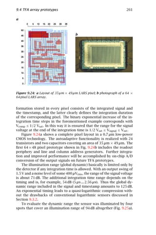


![264 9 Image Sensors in TFA (Thin Film on ASIC) Technology
a
b
VDD
VDD
VRef VRef
VDet
Hold Source follower
90fF
100fF
Detector Amplifier Readout
Reset 5fF 10fF
VRef
Figure 9.27: The star tracker: a detectable star magnitudes; and b pixel circuit.
optimization of the pixel circuitry a total time of down to 925 µs will
probably be achieved, which is sufficient for single-shot flash operation.
9.5.2 TFA star tracker
Imagers for space conditions inherently require special qualities such
as radiation hardness. Furthermore, in case of satellite attitude deter-
mination, stars with illumination intensities in the millilux or microlux
range have to be detected. Nevertheless, in contrast to terrestrial ob-
servatories, short irradiation times due to the satellite movement must
be taken into account. A TFA concept for a star tracker has been devel-
oped, employing a radiation hard silicon on insulator (SOI) technology
for the ASIC and a detector made of a-Si:H which proves to be more
radiation resistant than crystalline materials [30, 31, 32].
A suitable design for the star tracker has to handle extremely low
photocurrents in the femtoampere range and to convert the integrated
charge to a voltage [29]. The dark current can be minimized by op-
erating the detector close to short-circuit condition and by cooling,
which becomes obvious from Fig. 9.2a and b, respectively. Figure 9.27a
demonstrates the visual star magnitudes that can be detected with the
proposed star tracker, taking into account limitations due to dark cur-
rent. The specified minimum detectable magnitude is 4.75, which is
achieved at -0.1 V bias without or with moderate cooling.
As can be seen in the circuit diagram in Fig. 9.27b, early amplifi-
cation within the pixel is employed in order to minimize noise and
leakage current influence. The amplifier is designed as a simple cas-
code inverter, thus its input capacitance is minimized. The effective
integration capacitance therefore is determined mainly by the detec-
tor blocking capacitance. More sophisticated pixel circuitries such as
a current mirror similar to the one depicted in Fig. 7.9 provide higher
gain, but also aggravate leakage current effects. A source follower with
a common load for each column serves as driver element of the active](https://image.slidesharecdn.com/computervision-handbookofcomputervisionandapplicationsvolume1-sensorsandimaging-120205081125-phpapp02/85/Computer-vision-handbook-of-computer-vision-and-applications-volume-1-sensors-and-imaging-289-320.jpg)
![9.5 TFA array concepts 265
pixel. In the depicted pixel variant, the voltage at the inverter out-
put is sampled and held until the following integration period, hence
the integration time is not decreased by the time required for read-
out. Alternatively, the sample circuit is omitted if correlated double
sampling is employed. In this case the reset level and the subsequent
signal are read out, and the difference of these two signals is generated
outside the pixel. In this way reset noise and fixed-pattern noise are
efficiently suppressed, while flicker noise with its low cut-off frequency
is significantly reduced due to the high-pass characteristic of the CDS
procedure.
9.5.3 Hybrid a-Si:H/x-Si detector
The sensitivity of a space-based star sensor has to be as high as possible
in order to obtain a sufficient signal voltage. In a TFA sensor such as
the one discussed in Section 9.5.2 the photogenerated charge results in
a gate voltage V of the pixel amplifier:
Q
V= (9.5)
Cdet + Cin
For usual pixel sizes the detector capacitance Cdet is significantly larger
than the input capacitance Cin of the pixel circuit. However, as the
detector area is decreased in order to minimize Cdet , the sensitivity
and, therefore, Q decrease by the same factor. As a result, the signal
voltage is inherently limited by the detector technology.
Unlike the star sensor outlined in Section 9.5.2, the HYbrid DEtector
(HYDE) employs a charge storage principle similar to a CCD. Thus the
charge/voltage conversion is determined only by the readout stage that
can be designed to provide a low capacitance [29, 33]. As can be seen
in Fig. 9.28 the a-Si:H thin-film system is deposited on the rear side of
a thinned ASIC wafer that faces the incident light. The charge carriers
are collected in a MOS capacitance, which works in the same way as a
photogate in a CCD pixel. Photogeneration takes place in the a-Si:H as
well as—for longer wavelength photons—in the x-Si material. There-
fore, the advantages of both materials are combined to some degree. It
is obvious that this principle can also be employed to realize a hybrid
color detector, where the x-Si provides sensitivity for red light.
The HYDE offers the advantages of an increased charge amplifica-
tion and additional x-Si photosensitivity compared to conventional TFA
sensors. Moreover, the HYDE concept includes the substantial benefits
of TFA over CCD, because it allows CMOS circuit design and manufac-
turing in a standard technology. A similar pixel design as in Fig. 9.27b
can be employed for the HYDE. However, among other performance re-
strictions of a standard process, the ASIC wafer has to be thinned in
order to achieve a depletion region extending down to the amorphous](https://image.slidesharecdn.com/computervision-handbookofcomputervisionandapplicationsvolume1-sensorsandimaging-120205081125-phpapp02/85/Computer-vision-handbook-of-computer-vision-and-applications-volume-1-sensors-and-imaging-290-320.jpg)
![266 9 Image Sensors in TFA (Thin Film on ASIC) Technology
Oxide Store Transfer Out Reset VDD
Poly-Si
Al
Inversion n+ n+ n+
Depletion
π-x-Si
i-a-Si:H
p-a-Si:H
TCO Front
Figure 9.28: Cross section of the hybrid sensor HYDE.
Figure 9.29: Spectral responses of conventional and carbonized pin photodi-
odes in comparison to transmission of UV and visible light filters.
p-layer. Further research is required to determine whether the higher
sensitivity justifies the increased technological expenditure.
9.5.4 UV detector
Due to its wide bandgap, amorphous hydrogenated silicon is an ap-
propriate material for the fabrication of ultraviolet radiation (UV) de-
tectors. Compared to conventional pin diodes, carbonization and layer
thickness variation allow greater UV sensitivity. Figure 9.29 depicts the
photoresponses of a conventional a-Si:H pin photodiode and an a-SiC:H
pin device for near UV detection. To exclude visible light, which is in-
herently dominant for natural illumination, a combination of filters is
required. In this example, a UG11 is employed to suppress visible light;
however, the filter exhibits some transmittivity for near IR radiation. A
reference measurement with the UG11 and GG385 filters is necessary
to also eliminate this IR portion. Further optimization leads to a de-
vice with a maximum spectral response for UV radiation in the range
of 200 nm to 300 nm and no measurable sensitivity for visible light
[34]. In this way no filters are required to suppress visible light in a UV](https://image.slidesharecdn.com/computervision-handbookofcomputervisionandapplicationsvolume1-sensorsandimaging-120205081125-phpapp02/85/Computer-vision-handbook-of-computer-vision-and-applications-volume-1-sensors-and-imaging-291-320.jpg)

![268 9 Image Sensors in TFA (Thin Film on ASIC) Technology
sensors, as TFA employs standard technologies. Moreover, TFA tech-
nology may be an incentive for novel applications of image sensors.
The basic TFA concept provides two independent design flows for the
thin-film detector and the ASIC. Based on the customer’s specification,
circuit design, thin-film optimization and processing are performed by
the TFA manufacturer, while the ASIC fabrication is done by an ASIC
supplier. Market-ready TFA products are expected to be released within
two years.
Acknowledgment
The authors appreciate the cooperation of F. Blecher, A. Eckhardt, K.
Seibel and J. Sterzel of the Institute for Semiconductor Electronics, Uni-
versity of Siegen and S. Benthien, H. Keller, T. Lulé and M. Sommer
of Silicon Vision GmbH. The authors also wish to thank R. C. Lind, L.
Humm, M. Daniels, N. Wu and H. Yen of Delphi Delco Electronics Sys-
tems, U. Efron of Hughes Research Laboratories, F. Librecht and B. van
Uffel of AGFA-Gevaert N.V., C.-D. Hamann and B. Zerbe of Adam Opel
AG and E. Roth of Daimler-Benz Aerospace Jena Optronik GmbH for
useful discussions and technical support.
9.7 References
[1] Kemeny, S. E., Eid, E.-S., Mendis, S., and Fossum, E. R., (1991). Update
on Focal-Plane Image Processing Research, Charge-Coupled Devices and
Solid-State Optical Sensors II. Proc. SPIE, 1447:243–250.
[2] Mendis, S., Kemeny, S., Gee, R., Pain, B., Staller, C., Kim, Q., and Fossum, E.,
(1997). CMOS active pixel image sensors for highly integrated imaging
systems. IEEE J. Solid-State Circ., 32:187–197.
[3] Fischer, H., Schulte, J., Giehl, J., Böhm, M., and Schmitt, J. P. M., (1992).
Thin Film on ASIC—a Novel Concept for Intelligent Image Sensors. Mat.
Res. Soc. Symp. Proc., 285:1139–1145.
[4] Giehl, J., Stiebig, H., Rieve, P., and Böhm, M., (1994). Thin film on ASIC
(TFA)-color sensors. In New Applications of Optical Thin Film Detectors,
G. Hecht and J. Hahn, eds., pp. 560–563. Oberursel: DGM Informations-
gesellschaft Oberursel mbH.
[5] Schulte, J., (1996). Intelligente Bildsensoren in TFA-Technologie am Beispiel
eines Äquidensitenextraktors. PhD thesis, Universität-GH Siegen.
[6] Fischer, H., (1996). Ein analoger Bildsensor in TFA (Thin Film on ASIC)-
Technologie. PhD thesis, Universität-GH Siegen.
[7] Fischer, H., Schulte, J., Rieve, P., and Böhm, M., (1994). Technology and
performance of TFA (Thin Film on ASIC)-sensors. Mat. Res. Soc. Symp.
Proc., 336:867–872.](https://image.slidesharecdn.com/computervision-handbookofcomputervisionandapplicationsvolume1-sensorsandimaging-120205081125-phpapp02/85/Computer-vision-handbook-of-computer-vision-and-applications-volume-1-sensors-and-imaging-293-320.jpg)
![9.7 References 269
[8] de Cesare, G., Irrera, F., Lemmi, F., and Palma, F., (1995). Amorphous
Si/SiC three-color detector with adjustable threshold. Appl. Phys. Lett.,
66 (10):1178–1180.
[9] Eberhardt, K., Neidlinger, T., and Schubert, M. B., (1995). Three-color sen-
sor based on amorphous n-i-p-i-n layer sequence. IEEE Trans. Electron
Devices, 42 (10):1763–1768.
[10] Stiebig, H., Giehl, J., Knipp, D., Rieve, P., and Böhm, M., (1995). Amorphous
silicon three color detector. Mat. Res. Soc. Symp. Proc., 377:815–826.
[11] Tsai, H.-K. and Lee, S.-C., (1988). Amorphous SiC/SiC three-color detector.
Appl. Phys. Lett., 52 (4):275–277.
[12] Zhu, Q., Stiebig, H., Rieve, P., Fischer, H., and Böhm, M., (1994). A novel
a-Si(C):H nolor sensor array. Mat. Res. Soc. Symp. Proc., 336:843–848.
[13] Zhu, Q., Coors, S., Schneider, B., Rieve, P., and Böhm, M., (1998). Bias
sensitive a-Si(C):H multispectral detectors. IEEE Trans. Electron Devices,
45(7):1393–1398.
[14] Giehl, J., Zhu, Q., Rieve, P., and Böhm, M., (1996). Transient behavior of
color diodes. Mat. Res. Soc. Symp. Proc., 420:159–164.
[15] Rieve, P., Giehl, J., Zhu, Q., and Böhm, M., (1996). a-Si:H photo diode with
variable spectral sensitivity. Mat. Res. Soc. Symp. Proc., 420:135–140.
[16] Zhu, Q., Sterzel, J., Schneider, B., Coors, S., and Böhm, M., (1998). Transient
behavior of a-Si(C):H bulk barrier color detectors. Jour. Applied Physics,
83(7):3906–3910.
[17] Street, R. A., (1990). Thermal generation currents in hydrogenated amor-
phous silicon p-i-n structures. Appl. Phys. Lett., 57 (13):1334–1336.
[18] Zhu, Q., Stiebig, H., Rieve, P., Giehl, J., Sommer, M., and Böhm, M., (1994).
New type of thin film color image sensor, sensors and control for automa-
tion. SPIE Proc., 2247:301–310.
[19] Blecher, F., Seibel, K., and Böhm, M., (1998). Photo- and Dark Current
Noise in a-Si:H pin Diodes at Forward and Reverse Bias. Presented at MRS
Spring Meeting, San Francisco.
[20] Wieczorek, H., (1995). 1/f noise in amorphous silicon nip and pin diodes.
J. Appl. Phys., 77 (7):3300.
[21] Blecher, F. and Seibel, K., (1997). Simulation und experimentelle Verifika-
tion von statistischen Kenngrößen und Rauschmodellen a-Si:H basierter
optischer Sensoren. DFG-Abschlußbericht Bo 772/3-1.
[22] Boudry, J. M. and Antonuk, L. E., (1993). Current-noise-power spectra for
amorphous silicon photodiode sensors. Mat. Res. Soc. Symp. Proc., 297:
975–980.
[23] Böhm, M., Blecher, F., Eckhardt, A., Schneider, B., Benthien, S., Keller, H.,
Lulé, T., Rieve, P., Sommer, M., Lind, R. C., Humm, L., Daniels, M., Wu, N.,
and Yen, H., (1998). High Dynamic Range Image Sensors in Thin Film
on ASIC-Technology for Automotive Applications. Presented at Advanced
Microsystems for Automotive Applications, Berlin.
[24] Wong, H.-S. P., (1997). CMOS image sensors—recent advances and device
scaling considerations. Tech. Digest IEDM, 97:201–204.](https://image.slidesharecdn.com/computervision-handbookofcomputervisionandapplicationsvolume1-sensorsandimaging-120205081125-phpapp02/85/Computer-vision-handbook-of-computer-vision-and-applications-volume-1-sensors-and-imaging-294-320.jpg)
![270 9 Image Sensors in TFA (Thin Film on ASIC) Technology
[25] Schulte, J., Fischer, H., Lulé, T., Zhu, Q., and Böhm, M., (1994). Properties
of TFA (Thin Film on ASIC) sensors. In Micro System Technologies ´94,
A. H. H. Reichl, ed., pp. 783–790. Berlin: VDE-Verlag.
[26] Schneider, B., Fischer, H., Benthien, S., Keller, H., Lulé, T., Rieve, P., Som-
mer, M., Schulte, J., and Böhm, M., (1997). TFA image sensors: From the
one transistor cell to a locally adaptive high dynamic range sensor. Tech.
Digest. IEDM, 97:209–212.
[27] Lulé, T., Fischer, H., Benthien, S., Keller, H., Sommer, M., Schulte, J.,
Rieve, P., and Böhm, M., (1996). Image sensor with per-pixel pro-
grammable sensitivity in TFA technology. In Micro System Technologies
´96, A. H. H. Reichl, ed., pp. 675–680. Berlin: VDE-Verlag.
[28] Chen, S. and Ginosar, R., (1995). Adaptive sensitivity CCD image sensor.
Proc. SPIE, 2415:303–309.
[29] Böhm, M., Lulé, T., Fischer, H., Schulte, J., Schneider, B., Benthien, S.,
Blecher, F., Coors, S., Eckhardt, A., Keller, H., Rieve, P., Seibel, K., Som-
mer, M., and Sterzel, J., (1998). Design and Fabrication of a High Dynamic
Range Image Sensor in TFA Technology, to be presented at 1998 VLSI
Circuits Symposium, Honolulu.
[30] Hollingworth, R. E. and J. Xi, A. M., (1989). Proton and neutron damage in
thick amorphous silicon diodes. Mat. Res. Soc. Symp. Proc., 149:655–659.
[31] Woodyard, J. R. and Landis, G. A., (1991). Radiation resistance of thin-film
solar cells for space photovoltaic power. Solar Cells, 31:297–329.
[32] Boudry, J. M. and Antonuk, L. E., (1994). Radiation damage of amorphous
silicon photodiode sensors. IEEE Trans. Nuclear Science, 41(4):703–707.
[33] Schneider, B., Blecher, F., Eckhardt, A., Seibel, K., Sterzel, J., Böhm, M.,
Benthien, S., Keller, H., Lulé, T., Rieve, P., Sommer, M., Librecht, F., and van
Uffel, B., (1998). TFA Image Sensors—A Survey with Regard to Possible
Applications, presented at OPTO 98, Erfurt, Germany.
[34] Caputo, D., de Cesare, G., Irrera, F., and Palma, F., (1996). Solar-blind UV
photodetectors for large area applications. IEEE Trans. Electron Devices,
43 (9):1351–1356.](https://image.slidesharecdn.com/computervision-handbookofcomputervisionandapplicationsvolume1-sensorsandimaging-120205081125-phpapp02/85/Computer-vision-handbook-of-computer-vision-and-applications-volume-1-sensors-and-imaging-295-320.jpg)

![272 10 Poly SiGe Bolometers
10.1 Overview
The evolution of infrared (IR) sensors started during World War II, when
they were used mainly for night vision [1]. This application pushed
thermal imaging technology towards high spatial and temporal resolu-
tion and its use was extended to other fields such as fire control and
search track. Later, the spatial resolution of the detector was further
improved for scientific applications that included remote sensing of
earth resources [2] and astronomical exploration.
It is of some interest to follow the different development stages of
IR technology with time, as this sheds light on the limitations of dif-
ferent technologies and on how they were overcome. We consider, for
instance, early IR detectors, such as Golay pneumatic detectors [3], ra-
diation thermopiles [4], bolometers [5], and pyroelectric detectors [6].
Because the intensity of the IR radiation is deduced from the temper-
ature increase that it generates in the detector active element, these
devices are known as thermal detectors. The frequency response of
these detectors was limited by the large thermal mass of the active el-
ement; thus, they could not be used to produce a usable image with
raster scanning techniques. Hence, it appeared that the performance
of such detectors was limited by the laws of physics. Moreover, the at-
tachment of electrical leads, used to transfer the signal generated by the
detector to the electrical detection circuits, formed a highly conductive
thermal path that seriously degraded the sensitivity of the detector. As
a consequence, the use of thermal detectors was limited.
The development of semiconductor materials in the 1950s and
1960s provided photoconductor quantum detectors capable of sens-
ing photons with high electrical bandwidth. These detectors were used
mainly in military applications and, hence, they were designed specifi-
cally for near IR (1 to 3 µm), midwave IR (MWIR) (3 to 5 µm) and long-
wave IR (LWIR) (8 to 12 µm) regions. The response time of photo con-
ductor quantum detectors is determined by the free carrier lifetime
and is usually of the order of microseconds. Thus, it was possible to
integrate these detectors in arrays used for parallel scanned imaging
systems. Such arrays need cryogenic cooling to improve the thresh-
old sensitivity and to reduce the fundamental noise of the detector.
Moreover, high spatial resolution, which requires a large number of de-
tectors, was not achievable as the power dissipated in each detector,
and the heat load due to electrical wiring was too large. Later, develop-
ment of PN junction diode devices noticeably reduced the bias power
dissipation, as these devices act as a photovoltaic IR detector having
high impedance. In spite of this improvement, the number of detec-
tor elements was still limited by the number of interconnection leads
that could be used. This problem was solved by the development of
charge-coupled devices (CCD) and charge injection devices (CID), which](https://image.slidesharecdn.com/computervision-handbookofcomputervisionandapplicationsvolume1-sensorsandimaging-120205081125-phpapp02/85/Computer-vision-handbook-of-computer-vision-and-applications-volume-1-sensors-and-imaging-297-320.jpg)
![10.1 Overview 273
provided the possibility of multiplexing the IR detectors of a focal plane
array (FPA) and allowed packaging a large number of detectors in a
small practical sensor. Sensors, based on this technology are now avail-
able to cover the IR spectrum, with Si-based devices for the near IR (e. g.,
platinum silicide (Pt-Si) [7], indium antimonide (InSb) for MWIR [8] and
mercury cadmium telluride (HgCdTe) for LWIR [9]). Such detectors have
quantum efficiencies approaching the theoretical limit.
As quantum detectors must operate at low temperature, they are in-
serted in a radiative cooler, which is bulky, heavy, and delicate. This fact
causes important logistic problems, especially in military and space ap-
plications. Furthermore, a radiative cooler is expensive and this limits
the amplitude of the market for detection systems. These drawbacks
motivated the development of uncooled detectors.
Both quantum and thermal uncooled detectors have been realized.
Examples of the first type include lead sulfide (PbS) and lead selenide
(PbSe) detectors. Although they are somewhat slow, when combined
with modern readout electronics they have a sufficient bandwidth for
imaging operation with high sensitivity in the 1–5 µm region [10]. The
most important advances in the field of IR uncooled detectors have
been achieved with thermal detectors. The development of microma-
chining techniques [11] has allowed realization of detectors of small
size (50 µm and below), with low thermal capacity and large thermal
insulation. The combination of these latter two features gives high
responsivity and reasonably large cut off frequency. Several types of
thermal detectors operating at room temperature have been realized.
Pyroelectric and ferroelectric detectors have been developed by Texas
Instruments [12, 13, 14, 15, 16]. These detectors are essentially ther-
mally modulated electrical capacitors and can be operated uncooled
or in a temperature-stabilized mode. Their large detectivity compen-
sates for some drawbacks, such as the need of chopping IR radiation
and the difficulty of integration with the driving electronics on a sin-
gle chip (detectors must be bump-bonded to the silicon substrate [17]).
These drawbacks are not present in FPAs of resistor microbolometers
developed by Honeywell [18] and by the Australian organization DSTO
[19, 20, 21, 22, 23, 24]. They do not require modulated IR radiation and
can be integrated monolithically with the driving electronics. The high
frame rate capability of these microbolometer FPAs makes them well-
suited for automated moving target detection and tracking. Their low
cost and the low maintenance that they require enlarge the market of
IR cameras to a wide variety of civilian applications, including security,
automotive areas, rescue, and fire control.
In the following sections we shall focus on bolometers. In Sec-
tion 10.2, a general description of the principle of operation of bolome-
ters will be presented. This will include the different factors contribut-
ing to the temperature rise of the bolometer, the derivation of the re-](https://image.slidesharecdn.com/computervision-handbookofcomputervisionandapplicationsvolume1-sensorsandimaging-120205081125-phpapp02/85/Computer-vision-handbook-of-computer-vision-and-applications-volume-1-sensors-and-imaging-298-320.jpg)

![10.2 Principle of operation of bolometers 275
WIR
Bolometer
Rb
+
RL VL
I
−
V
Figure 10.2: Biasing circuit of a bolometer.
10.2.1 Thermal behavior
In this section, we analyze briefly the factors that make the bolometer
temperature larger than that of the heat sink. In general, the circuit
shown in Fig. 10.2 is used to bias the bolometer. The voltage source V
generates a current I that flows through the circuit; as a result, there is
power dissipation and the bolometer heats up. Moreover, the absorbed
IR radiation will also change the temperature of the bolometer. The
thermal balance is described by
dT
W =C + G(T − T0 ) (10.1)
dt
This equation simply states that a part of the power W (absorbed IR
plus dissipated electrical power) is used to heat the bolometer (first
term in RHS) and the rest flows towards the thermal sink (second term
in RHS).
First, we shall discuss the dependence of temperature on the inci-
dent radiation. In general, the incident radiation varies with time and
can be expressed as W = W0 + Wω ejωt , which is a superposition of a
constant component and a time-dependent component. The power ab-
sorbed by the bolometer is ˜W , where ˜ is the emissivity of the bolome-
ter. The temperature increase is ∆T = W0 /G + ∆Tac . The first term is
due to the constant power W0 while the second term is due to the time
dependent power and is expressed as [25]](https://image.slidesharecdn.com/computervision-handbookofcomputervisionandapplicationsvolume1-sensorsandimaging-120205081125-phpapp02/85/Computer-vision-handbook-of-computer-vision-and-applications-volume-1-sensors-and-imaging-300-320.jpg)

![10.2 Principle of operation of bolometers 277
a b
400 1.6
-9 R=50 K W
C=7 x 10 J/K
G=0.3 mW/K
1.2
Applied Voltage (V)
300
Time ( µ s)
200 0.8
100 0.4
0 0
0 0.2 0.4 0.6 0.8 1 0 25 50 75 100
∆T (K) ∆T (K)
Figure 10.3: a Time required to obtain a temperature increase ∆T at different
pulsed bias (Solid line 2 V, dashed-dotted line 3 V, dotted line 4 V, dashed-double-
dotted line 5 V). The value of the thermal capacitance is also reported in the
figure. b Applied dc bias vs the temperature increase that it generates in the
bolometer. Different curves refer to different activation energies. (Solid line
Ea = 0.16 eV, dotted line Ea = 0.32 eV, dashed dotted line Ea = 0.64 eV.) Values
of the resistance and thermal conductance used in the calculations are reported
in the figure.
Fig. 10.3a displays the time interval required to increase the temper-
ature of the bolometer by 1 K for different biasing voltages. The dif-
ferent parameters in this plot are α = 0.02 K−1 , Rb (T0 ) = RL = 50 kΩ,
and C = 7 × 10⁻⁹ J/K. As in actual operation the duration of the voltage
pulse is few µs (T < 10 µs), it is obvious that the use of pulsed bias
allows applying large voltages without appreciable heating.
On the other hand, when using dc bias, the temperature increase
is large and the change of TCR with temperature must be taken into
account. It is then more convenient to express the TCR in terms of
the activation energy Ea , which is temperature independent [26] and is
related to the TCR by Ea = kT 2 α. The associated temperature increase
can be evaluated directly from Eq. (10.1) at steady state. This yields the
following expression
W V 2 Rb
∆T = = 2
(10.4)
G G (Rb (T ) + RL )
To maximize the responsivity of the bolometer, the load resistor RL
must be equal to the bolometer resistance at the operation temperature,
hence, we assume RL = Rb (T ). Equation (10.4) is plotted in Fig. 10.3b
for G = 3 × 10⁻⁷ W /K, Rb (T0 ) = 50 kΩ and for different activation ener-
gies. It is evident that for high activation energies, there is a maximum](https://image.slidesharecdn.com/computervision-handbookofcomputervisionandapplicationsvolume1-sensorsandimaging-120205081125-phpapp02/85/Computer-vision-handbook-of-computer-vision-and-applications-volume-1-sensors-and-imaging-302-320.jpg)

![10.2 Principle of operation of bolometers 279
where we have used the relation α = (1/Rb )(dRb /dT ). α is a decreas-
ing function of temperature and its value at the operating temperature
must be used. It can be concluded from Eq. (10.9) that the responsivity
varies linearly with the biasing voltage; this is true only for pulsed bias,
when the TCR is nearly constant. Using dc bias, the increase of voltage
will be compensated by the decrease in TCR and the performance will
have an upper limit.
10.2.3 Sources of noise
Random noise plays an important role in the performance of bolome-
ters as it determines the minimum power that can be detected. The
noise sources may arise in the bolometer, in the incident radiation, or
in the electronic circuitry associated with the detection system. In this
section we shall discuss only the noise associated with the bolometer.
The major noise sources in bolometers are the thermal conductance
noise, the Johnson noise, and the low frequency (1/f ) noise.
We start by discussing fluctuations in the thermal conductance. As
described in the previous section, in absence of an external radiation
the temperature of the bolometer is the same as that of the heat sink
(T0 ). This means that on average the heat flow from the bolometer to
the heat sink is completely balanced by the heat flow in the opposite
direction. This is true only on the average, as there are instantaneous
fluctuations of the power flowing through the support into the detector.
Their root mean square (RMS) is given by ∆Wth = 4kT 2 G∆fth [27],
where ∆fth is the thermal noise bandwidth and is determined by the
inverse of the thermal time constant τ. These fluctuations in the power
generate fluctuations in the voltage Vth , the RMS value of which is given
by
Vth = R∆Wth = R 4kT 2 G∆fth (10.10)
The Johnson noise arises from the random motion of free carriers
within any resistive material. The RMS of the voltage fluctuation as-
sociated with the Johnson noise is [28]
VJ = 4kT Rb ∆fe (10.11)
where ∆fe is the electric bandwidth and is determined by the time in-
terval allocated to read the signal.
In any resistor, it is possible to measure as noise a component that
decreases as 1/f γ (where 0 ≤ γ ≤ 0.5) and which adds up to the John-
son noise. Thus, as its origin is still a matter for debate, it is well
described by an empirical expression due to Hooge [29]](https://image.slidesharecdn.com/computervision-handbookofcomputervisionandapplicationsvolume1-sensorsandimaging-120205081125-phpapp02/85/Computer-vision-handbook-of-computer-vision-and-applications-volume-1-sensors-and-imaging-304-320.jpg)
![280 10 Poly SiGe Bolometers
ρ
Vn,1/f = KVb (10.12)
W Ltf
where K is a constant that depends on the type of material, Vb is the
voltage applied to the bolometer, W , L, and t are, respectively, the
width, length, and thickness of the active part of the bolometer.
The total noise of the bolometer Vn is the RMS of these three noise
components and it is given by
2 2 2
Vn = Vth + VJ + V1/f (10.13)
Normally the noise component due to fluctuations in thermal conduc-
tance is negligible. Material properties, frequency bandwidth, and bias
voltage determine whether the 1/f noise or the Johnson noise domi-
nates.
The performances of the detector are characterized by the ratio of
voltage noise to responsivity, or more precisely by the noise equivalent
power (NEP), which is the power required to produce a unity signal to
noise ratio and is given by
Vn
NEP = (10.14)
R
10.3 Microbolometer focal plane arrays
The development of silicon-based, uncooled, focal plane arrays of mi-
crobolometers started after the Gulf War, as the current imaging em-
ploying visible light cameras, low-light level, image intensified, or con-
ventional IR cameras had serious deficiencies. Visible TV cameras re-
quire well-lighted areas and can not image in darkness. Low-level light
TV cameras have difficulties when operating in bright sunlight or in
total darkness. Image intensifiers require some ambient light. Conven-
tional IR cameras are costly, require an initial cool-down period and
need additional power for the cooling pump or a periodic gas replen-
ishment for long-term operation. Meanwhile, uncooled FPA operating
in the 8-12-µm range combine the capability of operation in bright sun-
light or total darkness, typical to IR cameras, of low cost, light weight,
and ease of use.
Depending on the technology used for integrating the detectors with
the readout electronics, FPA are called hybrid or monolithic. Hybrid
arrays are realized by bump-bonding the detectors to a silicon micro-
circuit; this is the case of ferroelectric detectors [17], where monolithic](https://image.slidesharecdn.com/computervision-handbookofcomputervisionandapplicationsvolume1-sensorsandimaging-120205081125-phpapp02/85/Computer-vision-handbook-of-computer-vision-and-applications-volume-1-sensors-and-imaging-305-320.jpg)
![10.3 Microbolometer focal plane arrays 281
arrays are obtained by directly preparing the detector and the readout
microcircuit on the same silicon chip [30]. The two principle routes
of monolithic technology development are thin pyroelectric or dielec-
tric bolometers and resistance bolometers. The former technology is
less mature due to the need to develop materials fully compatible with
silicon wafer processing. Meanwhile, there are many materials suitable
for resistance bolometers, which can be readily integrated with VLSI mi-
crocircuits. Moreover, ferroelectric arrays have only ac response and
require choppers to operate in a slowly changing scene [31]. This fea-
ture increases system complexity and decreases the SNR by a factor
of 1.4, as the thermal radiation signal is blocked on every other frame
basis. Also, the sensor internal frame rate is augmented by a factor
of two, which yields a decrease of the SNR of an additional factor of
1.4. Resistance bolometers can be used in dc mode and do not imply
choppers.
Focal plan arrays of microbolometers were first developed by Honey-
well [30]. Micromachining techniques were used to realize large arrays
(240 × 336) of detectors operating in the range 8–12 µm. The active ele-
ment is made of vanadium oxide. The FPA readout is at 30 Hz and does
not utilize a chopper. The array can detect a temperature difference
of 0.1 K between two elements of the scene. The thermal insulation
between pixels is less than -142 dB, which means that a 1000 °C target
directed toward a certain pixel will have in adjacent pixels an effect that
is 8 × 10⁻⁸ less. Such a feature makes blooming virtually nonexistent.
Each FPA is a single chip monolithically integrated with multiplexers
for simplicity and affordability. The driving electronics for such arrays
are realized by bipolar transistor technology. Recent uncooled arrays
developed by Honeywell and Rockwell have been integrated with CMOS
circuitry [32]. These arrays have a frame rate of 60 Hz and the minimum
detectable temperature difference on the scene is 0.07 K. Similar arrays,
using vanadium oxide as the temperature-sensitive element, have been
developed by Amber [33] and Loral Infrared and Imaging Systems [34].
10.3.1 Model describing the performance of FPA
In this subsection we briefly analyze the different quantities affecting
the performance of FPA. To achieve this goal, we shall present a model
describing the performance of an IR camera consisting of 640 × 480
pixels and operated at a frame rate of 20 Hz. The biasing circuit for
each pixel is shown in Fig. 10.4; all noise sources are indicated in the
figure. Here Vb,th , Vb,J and Vb,1/f represent, respectively, the thermal
conductance noise, the Johnson noise, and the 1/f noise of the bolome-
ter; in addition, VL,J is the Johnson noise of the load resistor and Va
the noise of the amplifier.](https://image.slidesharecdn.com/computervision-handbookofcomputervisionandapplicationsvolume1-sensorsandimaging-120205081125-phpapp02/85/Computer-vision-handbook-of-computer-vision-and-applications-volume-1-sensors-and-imaging-306-320.jpg)
![282 10 Poly SiGe Bolometers
WIR
Bolometer
Vb, J Vb,1/f
Rb
VL, J
Vb, th
Va +
RL A
V
−
V
Figure 10.4: Biasing circuit of a camera pixel. The different sources of noise
are also reported in the figure.
We first concentrate on the noise introduced by the amplifier, which
has two main components: 1/f and Johnson. The 1/f noise can be
expressed as [28]
1/2
Va,1/f = Sa,1/f ln(4fmax /fmin ) (10.15)
where Sa,1/f depends on the type of amplifier used, fmax and fmin are
the extremes of the bandwidth. The Johnson noise is given by Laker
and Sansen [28]
Va,J = Sa,J ∆fe (10.16)
where Sa,J = 8kT /3gm , gm is the transconductance of the amplifier
and ∆fe = fmax − fmin is the bandwidth of the amplifier.
Two solutions are available for amplifying the signal: to use a built-
in amplifier for each pixel or to use one or more external amplifiers.
We will briefly discuss advantages and disadvantages of the two. For
a good external commercial amplifier, for example, OP-27, the value of
1/2 1/2
S1/f is on the average 5 nV, while Sa,J = 3 nV.
An estimate of the noise characteristics of an internal amplifier can
be obtained by assuming that the amplifiers are built by CMOS transis-
tors having the following properties:
channel width W = 10 µm,
channel length L = 5 µm,
oxide thickness tox = 0.2 µm,
oxide permittivity ox = 3.45 × 10⁻¹¹ F/m, and
carrier mobility µn = 0.08 m2 /Vs.](https://image.slidesharecdn.com/computervision-handbookofcomputervisionandapplicationsvolume1-sensorsandimaging-120205081125-phpapp02/85/Computer-vision-handbook-of-computer-vision-and-applications-volume-1-sensors-and-imaging-307-320.jpg)
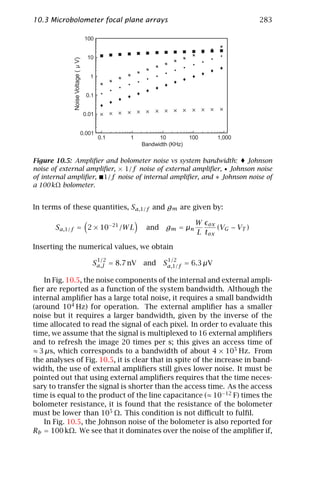
![284 10 Poly SiGe Bolometers
as suggested by the previous discussion, an external amplifier is used.
We conclude then that the performances of the FPA are dominated by
the noise of the bolometer more than from that of the amplifier.
Finally, the total noise generated at the input of the amplifier is
expressed as
1/2
2 2 2 2
Vn = ξ 2 (Vb,J + VL,J + Vb,1/f ) + Vb,th + Va
2
(10.17)
where ξ = RL /(Rb + RL ) represents the fraction of the noise at the input
of the amplifier.
10.3.2 Noise equivalent temperature difference
The performance of the camera is evaluated by its ability to detect slight
temperature changes of the scene. If the temperature of the scene is
changed from T0 to T0 + ∆T , the power reaching the detector will be
changed by [35]
Adet (∂M/∂T )∆T
∆Wdet = 2
(10.18)
4f#
where Adet is the area of the detecting pixel, ∂M/∂T is the thermal
contrast, and f# is the f -number of the imaging system defined by
focal length
f# = (10.19)
entrance of the pupil diameter
The noise equivalent temperature difference (NETD) is defined as the
temperature change of the scene that results in a change in the detected
power equal to the noise equivalent power (NEP), thus,
2
4f# NEP
NETD = (10.20)
Adet (∂M/∂T )
This model will be used in Section 10.6 to evaluate the performance of
poly SiGe FPAs and to compare them to those of vanadium oxide and
metal bolometers.
10.4 Bolometer materials
In this section, we describe which physical properties make a material
suitable for IR bolometers. We review the materials most commonly
used and analyze the advantages of using poly SiGe.](https://image.slidesharecdn.com/computervision-handbookofcomputervisionandapplicationsvolume1-sensorsandimaging-120205081125-phpapp02/85/Computer-vision-handbook-of-computer-vision-and-applications-volume-1-sensors-and-imaging-309-320.jpg)

![286 10 Poly SiGe Bolometers
10.4.2 Materials used for bolometers
Both metals and semiconductors have been used as active element de-
posited on an insulating membrane. In spite of their low TCR, metals
such as gold (TCR0 = 0.15 %)1 [36], platinum (TCR0 = 0.25 %) [37, 38], ti-
tanium (TCR = 0.2 %) [39, 40] have been used to provide low cost thermal
imaging in industrial automation and in security and safety systems.
These applications usually do not require the high infrared sensitivity
demanded by military purposes. Metal bolometers are characterized
by having low 1/f noise [39] and low thermal capacity, which means
low thermal time constant (τ < 1 ms [19]). The responsivity of titanium
bolometers is√ the order of 104 V/W and the maximum detectivity is
of
6.3 × 109 cm Hz/W [39].
The performance of bolometers can be improved by using semicon-
ductor materials. With respect to metals, they have a TCR about one
order of magnitude larger but also larger 1/f noise and resistivity. To
date, the best results have been obtained using vanadium oxide, which
is an amorphous film deposited by the ion beam sputtering process
where tight control of the oxygen content is maintained. High TCR
can be obtained at relatively low resistivity (−2 % for a sheet resistance
of 13.5 KΩ/sq for typically used thickness [41]). Noise in vanadium
oxide can be reduced by reducing the void content [42]. Using an op-
timized material, an NETD of about 75 mK for a 324 × 240 array made
of 50 µm × 50 µm pixels [43] has been achieved. Such low noise level
made vanadium oxide widely used in resistance bolometers and other
applications requiring high TCR [44, 45, 46, 47, 48]. It should be noted
that noise and TCR in vanadium oxide depend strongly on the prepara-
tion conditions, thus, a complicated optimization process is necessary
to achieve the required performance level. Furthermore, the material,
thus being compatible with post-processing of wafers already contain-
ing the readout electronics, is certainly not standard in IC technology
and foundries with the capability of depositing vanadium oxides are not
easily found. Other semiconductor materials, such as plasma chemical
vapor-phase deposited amorphous silicon [49], amorphous germanium
[50] and amorphous silicon carbide [51], have been used as the active
element of bolometers deposited on top of an insulating membrane.
These materials have TCR around −2 %, but they have a high 1/f noise
component.
10.4.3 Poly SiGe as a bolometer material
As already mentioned, the use of self-sustained suspended bolometers
provides a simpler technology, but is more demanding from the point
of view of material properties. The common material used for such
1 TCR is the Temperature Coefficient of Resistance at 20 °C.
0](https://image.slidesharecdn.com/computervision-handbookofcomputervisionandapplicationsvolume1-sensorsandimaging-120205081125-phpapp02/85/Computer-vision-handbook-of-computer-vision-and-applications-volume-1-sensors-and-imaging-311-320.jpg)
![10.4 Bolometer materials 287
technology is poly Si [52]. The performances of realized devices are
not comparable with those obtained using vanadium oxide, mainly be-
cause of the high thermal conductance of poly Si [53]. Furthermore,
the control of the stress in poly-Si requires high-temperature annealing
[54], which does not allow post-processing of the bolometer.
In this work, we introduce poly SiGe as a new material for bolome-
ters. The most attractive point in using poly SiGe is that its thermal
conductivity is at least a factor of five lower than that of poly Si [53]. To
clarify this issue, we consider the heat transport mechanism in lowly
doped semiconductors, which is due mainly to phonons, as the elec-
tronic contribution is negligible. The observation of a finite thermal
conductivity is due to the existence of different of phonon scattering
processes, the most important of which are:
1. Phonon-phonon scattering (two phonons interact to give a third
phonon, the total momentum is either conserved or changed by a
reciprocal lattice vector) [55];
2. Phonon scattering due to interaction with electron (or holes) [55];
3. Point-defect scattering [56]; and
4. Grain boundary scattering [57].
Mechanisms (1) and (2) are always present and their discussion is
not relevant for our purposes. Mechanism (3) is very important. This
kind of scattering is due to the presence of foreign atoms in substitu-
tional positions in the lattice. They are capable of hindering the prop-
agation of elastic waves in the solid. As an example, this mechanism
is responsible for the decrease of thermal conductivity when dopants
are added (notice that at high doping levels, the thermal conductiv-
ity increases again due to the increase of the electronic contribution).
Moreover, this mechanism reduces the thermal conductivity of alloys,
which is the case for silicon germanium (germanium atoms can be con-
sidered as point defects in the silicon lattice). The minimum thermal
conductance of poly SiGe is obtained at a germanium content of 30 %
[58]. Thus, we shall use this germanium concentration in preparing
poly SiGe bolometers. Mechanism (4) is also very important as it is
thought to be responsible for the lower thermal conductivity of poly
Si with respect to c-Si [53]. Preliminary data on poly SiGe shows that
its thermal conductivity is a factor of two lower than that of c-SiGe
(see Section 10.6.2). Low thermal conductivity, when combined with
thin supports, will greatly improve the performance of self-suspended
bolometers.
Poly SiGe has been prepared by chemical vapor deposition (CVD)
from a mixture of germane and diclorosilane at atmospheric or reduced
(40 torr) pressure. These two types of material will be indicated, respec-
tively, as APCVD and RPCVD. The chemical vapor deposition, especially](https://image.slidesharecdn.com/computervision-handbookofcomputervisionandapplicationsvolume1-sensorsandimaging-120205081125-phpapp02/85/Computer-vision-handbook-of-computer-vision-and-applications-volume-1-sensors-and-imaging-312-320.jpg)
![288 10 Poly SiGe Bolometers
Figure 10.7: Process flow for the fabrication of poly SiGe bolometers (a, b, c
are explained in the accompanying text; see Section 10.5.1).
at low pressure (LPCVD), is a technique largely used in microelectronics;
poly SiGe is a material compatible with standard IC processes. More-
over, it has been shown that the stress can be tuned to the required
value at relatively low temperatures (650 °C) [59], meanwhile similar
stress can be realized in poly Si at temperatures higher than 850 °C
[59]. Unlike vanadium oxide, the electrical properties of poly SiGe are
less sensitive to the deposition conditions, which means a simpler and
more easily transferable technology.
10.5 Poly SiGe bolometers
In this section, we will describe the process for realizing poly SiGe
bolometers. The different types of IR absorbers will be discussed. It
will be shown that selecting the best type of absorbers is a compro-
mise between high emissivity and low thermal capacity. Finally, we will
describe in detail the absorber used for poly SiGe bolometers.
10.5.1 Process for fabrication of poly SiGe bolometers
In this section we shall demonstrate the process required for realiz-
ing poly SiGe bolometers using surface micromachining techniques. In
brief, it consists of depositing the active layer onto a sacrificial layer,
which is etched away at the end of the process. In this way, the active
layer will be suspended and connected to the substrate only through](https://image.slidesharecdn.com/computervision-handbookofcomputervisionandapplicationsvolume1-sensorsandimaging-120205081125-phpapp02/85/Computer-vision-handbook-of-computer-vision-and-applications-volume-1-sensors-and-imaging-313-320.jpg)
![10.5 Poly SiGe bolometers 289
a b
Figure 10.8: An SEM picture of poly SiGe bolometers: a 50 µm × 50 µm pixel,
poly SiGe layer is 1 µm thick and the supports are 1 µm wide. b 25 µm × 25 µm
pixel, poly SiGe layer is 0.5 µm thick and the supports are 0.6 µm wide.
thin supports. The sacrificial layer that we have chosen is TEOS, as it
can be etched selectively with a high etch rate with respect to poly SiGe.
The different steps of the process are presented in Fig. 10.7. First
a TEOS layer having a thickness of 1 µm is deposited on top of an N-
type epi substrate. After TEOS deposition, the anchor points of the
active element to the substrate are patterned (refer to Fig. 10.7a). This
is followed by the deposition of poly SiGe (see Fig. 10.7b). The required
TCR is obtained by ion implanting poly SiGe with the appropriate dose
(in the range 1.5 ×10¹³ to 9 ×10¹³ boron/cm2 ). For a given TCR, the
thickness of poly SiGe is an important factor that decides the electrical
resistance and thermal conductance of the structures. The thicker the
layer, the lower the electrical resistance and the higher the thermal
conductance. In our process the thickness of the active element varied
from 0.25 µm to 1 µm.
As poly SiGe is transparent to IR radiation, an absorber layer must
be deposited. We will see later that this layer is electrically conductive.
In order to insulate the absorber electrically from the active element,
a thin insulator layer is deposited on top of poly SiGe (see Fig. 10.7b).
This layer is selected to be SiN having a thickness of 100 nm.
To transfer the electrical signal generated by the bolometer to the
driving electronics, the support must be highly doped. This is achieved
by a dose of 1016 boron/cm2 . This doping also forms a p-n junction
with the substrate providing electrical insulation. Metal contacts are
then deposited. Finally, the sacrificial layer is etched away using stan-
dard "freeze out" techniques [60, 61]. This step is shown schematically
in Fig. 10.7c.](https://image.slidesharecdn.com/computervision-handbookofcomputervisionandapplicationsvolume1-sensorsandimaging-120205081125-phpapp02/85/Computer-vision-handbook-of-computer-vision-and-applications-volume-1-sensors-and-imaging-314-320.jpg)
![290 10 Poly SiGe Bolometers
We have designed several structures having lateral dimensions vary-
ing from 50 µm × 50 µm down to 25 µm × 25 µm. An SEM picture of
some devices is displayed in Fig. 10.8. The thicknesses of poly SiGe lay-
ers for these devices are, respectively, 1 µm and 0.5 µm. The support
width is 1 µm for 50 µm × 50 µm and 0.6 µm for the 25 µm × 25 µm.
The holes on top of the structures are introduced to enhance etching of
the sacrificial layer. The absorbers shown in the figure will be explained
in detail in the next section.
10.5.2 IR absorbers
The function of the absorber is to convert the incident IR radiation into
heat. It must have high absorption efficiency and high reproducibil-
ity and must be compatible with standard processes. Furthermore, its
thermal mass must be low, compared to the thermal mass of the active
element. Different materials and different structures can be designed
to achieve 100 % absorption. Examples are metal black coatings, very
thin metal coatings, and quarter-wavelength structures.
Metal black coating has a significant absorption in the visible and
near IR regions. It has been shown that 80 % absorption, at 1 µm, can
be achieved for a thick bismuth black deposited on top of glass [62]. A
92–98 % absorption efficiency, in the range 8–14 µm, has been claimed
for platinum black absorbers, few µm thick [63]. The main disadvan-
tages of this type of absorber are its large thermal capacity, and the
low compatibility of the method used for coating with the fabrication
of the other elements of the array.
Thin metal film absorbers has been used in thermal detectors for
a long time [64]. The sheet resistance of the metal film is adjusted
to the value R = Z0 /2, where Z0 = µ0 / 0 = 377 Ω is the free space
impedance. Such an adjustment of R gives maximum absorption (50 %)
at long wavelengths. It should be noted that such low values for the
sheet resistance requires the deposition of a very thin layer (few tens
of Angstrom), which is difficult to realize in a uniform and controllable
way. This type of absorber is more feasible if metals having relatively
high resistivity are used. An example of such metals is NiCr, where
the desired sheet resistance is achieved for a layer 5-nm thick. An
alternative is to use a quarter-wavelength structure, which improves the
absorption of thin films from 50 % to 100 %, by backing the film with a
perfect reflector at a λ/4 optical distance. When using this absorber, the
different materials composing the absorber should have relatively low
thermal mass so as not to slow down the performance of the detector.](https://image.slidesharecdn.com/computervision-handbookofcomputervisionandapplicationsvolume1-sensorsandimaging-120205081125-phpapp02/85/Computer-vision-handbook-of-computer-vision-and-applications-volume-1-sensors-and-imaging-315-320.jpg)
![10.5 Poly SiGe bolometers 291
b
100
a
Thin metal 80
film (NiCr)
Absorbance (%)
60
λ
d= 40
4n
Dielectric
(Polyamide) 20
Reflector
(Titanium) 0
0 5 10 15 20
Wavelength ( µ m)
Figure 10.9: a Schematic of the quarter-wavelength absorber; b Dependence of
the IR absorber emissivity on wavelength. Full line: experimental data, dotted
line: fit according to Eq. (10.21).
10.5.3 Quarter-wavelength absorber
We shall discuss in detail the materials and characteristics of quarter-
wavelength absorbers [65] as this is the one that we used in poly SiGe
bolometers. The absorber is composed of a thermally evaporated tita-
nium layer (0.2 µm thick), a polyamide layer of thickness d and a resis-
tive nickel chromium (NiCr) absorber film having a sheet resistance Rf .
A cross section of this absorber is shown schematically in Fig. 10.9a.
The absorbance ˜ of such structure is given by [65]
4f
˜(d, α, Rf ) = (10.21)
(f + 1)2 + n2 cot2 (2π nd/λ)
where f = 377/Rf , n is the refractive index, λ is the wavelength of
the incident radiation. It is clear from Eq. (10.20) that the absorbance
is controlled mainly by the sheet resistance of the absorbing film and
by the thickness of the dielectric layer. It is possible to achieve 100 %
absorbance for certain wavelength (λ = 4nd), if the absorbing film is
matched to the free space (Rf = 377 Ω/sq).
For bolometer applications, we are interested in the wavelength re-
gion from 8 µm to 14 µm, which corresponds both to the maximum of
the emission of a blackbody at 300 K and to a transmission window
of the atmosphere [66]. As the refractive index of polyamide is 1.8,
then its thickness should be around 1.4 µm to achieve maximum ab-
sorbance at 10 µm. The measured emissivity of the realized absorber
is given by the solid line in Fig. 10.9. The behavior of the absorbance,
calculated from Eq. (10.21) using Rf = 320 Ω/sq and dielectric thick-
ness of 1.25 µm, is reported in Fig. 10.9 (see the dotted line), which
gives good agreement with experimental data. The thermal capacity
of this absorber is 2.4 J/m2 K, which is reasonably good as compared](https://image.slidesharecdn.com/computervision-handbookofcomputervisionandapplicationsvolume1-sensorsandimaging-120205081125-phpapp02/85/Computer-vision-handbook-of-computer-vision-and-applications-volume-1-sensors-and-imaging-316-320.jpg)
![292 10 Poly SiGe Bolometers
to that of other alternatives as platinum black has a thermal capac-
ity varying from 1.6–9.9 J/m2 K. Moreover, the process of realizing the
quarter-wavelength absorber is simpler and more reproducible as com-
pared to metal black coatings.
10.6 Characterization of poly SiGe bolometers
In this section, we present a complete characterization of poly-SiGe-
based bolometers. This includes the electrical, thermal, mechanical,
and optical properties. In Section 10.6.1, the effect of boron doping on
TCR and resistivity will be investigated over a doping range extending
from 1.5 × 10¹³ boron/cm2 to 9 × 10¹³ boron/cm2 . The procedure for
measuring the thermal conductance of fabricated bolometers will be
demonstrated in Section 10.6.2. The value of thermal conductivity of
poly SiGe will be deduced and compared to that of poly Si. The depen-
dence of stress in poly SiGe films on both the annealing temperature
and deposition conditions will be presented in Section 10.6.3. It will
be shown that the optimum value of stress can be obtained at 650 °C
by adjusting the deposition conditions. These values will be compared
to those typically found for poly Si. In Section 10.6.4, the procedure
for measuring both the responsivity and noise of the device will be dis-
cussed. It will be shown that it is possible to achieve a responsivity of
about 105 V/W. It will be demonstrated that the 1/f noise is the domi-
nant noise component. The effect of the deposition conditions of poly
SiGe on the 1/f noise will be investigated and possibilities for reduc-
ing this noise component will be discussed. It will be shown that an
√
average detectivity of about 2 × 109 cm Hz/W can be achieved.
10.6.1 TCR of poly SiGe
In general, conduction in poly crystalline materials is a thermally acti-
vated process [26] and, hence, the resistivity can be expressed as
ρ(T ) = ρ0 eEa /kT (10.22)
where Ea is the activation energy. The performance of the bolometer
depends mainly on the TCR, which measures the change in the resis-
tance corresponding to a temperature increase of one degree. The TCR
is related to the activation energy by
Ea
T CR = − (10.23)
KT 2
It is clear from Eq. (10.23) that high sensitivity corresponds to large
activation energies. The activation energy depends on the doping con-](https://image.slidesharecdn.com/computervision-handbookofcomputervisionandapplicationsvolume1-sensorsandimaging-120205081125-phpapp02/85/Computer-vision-handbook-of-computer-vision-and-applications-volume-1-sensors-and-imaging-317-320.jpg)
![10.6 Characterization of poly SiGe bolometers 293
0
-0.2
Log (ρ(T )/ρ(To ))
-0.4
-0.6
-0.8
2.6 2.8 3 3.2 3.4
1/T (x 10-3 ) (K-1 )
Figure 10.10: Logarithm of the ratio between the resistance at temperature T ,
and the room temperature resistance vs the inverse of the absolute temperature
for samples having different resistivity. Symbols: experimental data, solid line:
fit according to Eq. (10.22)). (• ρ(T0 ) = 17.45Ω cm, α0 = −2.45 %; ρ/T0 ) =
8.64Ω cm, α0 = −2.11 %; ρ(T0 ) = 1.97Ω cm, α0 = −1.28 × ρ(T0 ) = 0.97Ω cm,
α0 = −0.96 %).
centration, the grain size, and the density of defects at the grain bound-
aries [26].
The activation energy of poly SiGe was experimentally determined
by measuring the electrical current as a function of temperature, for
constant voltage. Figure 10.10 displays the temperature dependence
of the resistance of 1 µm thick poly SiGe layers ion implanted with 1.5
×1013 , 3 × 10¹³ , 6 × 10¹³ , and 9 × 10¹³ boron atoms / cm2 . The closed
circles represent the measured data, while the straight lines represent
a linear fit based on Eq. (10.22). From the slope of the line we can
determine the activation energy, and hence, the TCR at any temperature
can be computed from Eq. (10.23). The resistivity varies from 17.45
to 0.973 Ω cm, meanwhile, the TCR varies from −2.54 %/K to −1 %/K.
The selection of the optimal doping dose, stems from a compromise
between high TCR (low dose) and low noise (high dose), and it is the
value that minimizes the NETD of the array. This will be clarified in
Section 10.6.5.
It is interesting to compare the forementioned electrical properties
with those of poly Si. Also, in poly Si the TCR and resistivity depend on
the deposition conditions. For micromachining applications, as is the
one of bolometers, deposition conditions are set by the requirement of
low stress. The stress in LPCVD poly Si can be reduced by reducing the
deposition temperature to 590 °C. In this case poly Si is deposited in the
amorphous state and it crystallizes in the furnace during deposition.
The TCR for this material (when doped at 3 × 10¹³ boron/cm2 ) has been
found to be −2.87 % and the resistivity is 39.2 Ω cm. Comparing this](https://image.slidesharecdn.com/computervision-handbookofcomputervisionandapplicationsvolume1-sensorsandimaging-120205081125-phpapp02/85/Computer-vision-handbook-of-computer-vision-and-applications-volume-1-sensors-and-imaging-318-320.jpg)
![294 10 Poly SiGe Bolometers
result to those obtained for poly SiGe, it can be deduced that poly SiGe
has higher activation energy than poly Si, for the same resistivity. This
feature allows reducing the resistivity of the material, thus maintaining
a reasonable sensitivity.
10.6.2 Thermal conductivity of poly SiGe
Due to the role that thermal insulation plays in the performance of
the device, it is important to measure exactly its value. To this aim
two different procedures can be used. The first is based on applying a
wide voltage pulse (T τ) and on measuring the power dissipated and
the corresponding temperature rise of the bolometer, at steady state.
The other approach is based on determining the time constant of the
device from the dependence of the detected IR signal on frequency.
This approach requires the knowledge of the thermal capacity of the
structure and it will be discussed in Section 10.6.4.
In this section, we shall describe the first method. The experiment
is performed in vacuum, and without IR radiation. The bolometer is
biased at different Vb and the current Ib flowing through it is measured.
A power W = Ib Vb is dissipated in the bolometer. At steady state, the
thermal conductance G and the power W are related by
W = G(T − T0 ) (10.24)
where T0 is the room temperature and T is the temperature of the
bolometer. The temperature T can be easily evaluated by manipulating
Eq. (10.22) if the activation energy, the resistance at room temperature,
R(T0 ), and the resistance at the temperature T , R(T ), are known. It is
expressed as
T0
T = kT0 R(T )
(10.25)
1+ Ea ln R(T0 )
The resistance of the bolometer R(T ) is simply computed as Vb /Ib . The
value of R(T0 ) is computed in the same way but a narrow voltage pulse
(T τ) is applied, so that the bolometer is not heated. In Fig. 10.11,
the values of W vs (T − T0 ), obtained for different bias are plotted
for 25 µm × 25 µm pixels realized using 1 µm poly SiGe films, having
support width of 0.6 µm and support length of 10 µm or 20 µm. From
the slope of the straight line fitting these data we can compute the
thermal conductance of the structures. It is clear from the figure that
as the supports become longer the thermal insulation of the device is
improved.
It should also be noted that the thermal conductance in this case is
comparable to that achieved by insulating membranes (10−7 W/K [41]).](https://image.slidesharecdn.com/computervision-handbookofcomputervisionandapplicationsvolume1-sensorsandimaging-120205081125-phpapp02/85/Computer-vision-handbook-of-computer-vision-and-applications-volume-1-sensors-and-imaging-319-320.jpg)
![10.6 Characterization of poly SiGe bolometers 295
20
15
Power ( µ W)
10
5
0
0 10 20 30 40 50
Temperature Increase (K)
Figure 10.11: Power dissipated in the bolometer vs the temperature rise that
it generates in the bolometer itself. The two curves refer to bolometers having
thermal conductance G = 1.81 × 10⁻⁷ W/K (•) and G = 3.2 × 10⁻⁷ W/K ( ).
This means that using poly SiGe together with advanced lithographic
techniques allows for achievement of high thermal insulation by means
of a simpler technology. In order to relate the thermal conductance of
the device to the thermal conductivity g of the material and to the ge-
ometry of the supports, we have performed a finite element analysis
using the ANSYS simulator. Simulations were done by considering a
uniform heat generation over the active area of the bolometer. Agree-
ment between the simulated and experimental data was obtained for a
value of g = 2.7 W/mK. Thermal simulations have shown that for wide
(2 µm) and short (5 µm) supports, there is a significant temperature
drop at the active area. When the supports become thin and long the
thermal conductivity g of the material is, as expected, related to the
thermal conductance of the structure by G = gA/l, where A and l are,
respectively, the cross-sectional area and the length of the supports.
It should be noted also that the value of thermal conductivity of poly
SiGe, which we found, is lower than that of crystalline SiGe (5 W/mK
[58]). As previously discussed, we believe that this effect is due to grain
boundary scattering.
10.6.3 Mechanical properties of poly SiGe
The mechanical stability of the device is affected by the total stress of
the suspended structure. This includes the stress in the active element
and in the absorber layers. In general, the absorber could have either
tensile or compressive stress, which should be compensated by the ac-
tive element. This means that it should be possible to tune the stress
of the active element to be either compressive or tensile. It is advisable
to carry out this tuning at relatively low temperatures. To clarify this
issue, the effect of annealing on stress induced in poly SiGe deposited](https://image.slidesharecdn.com/computervision-handbookofcomputervisionandapplicationsvolume1-sensorsandimaging-120205081125-phpapp02/85/Computer-vision-handbook-of-computer-vision-and-applications-volume-1-sensors-and-imaging-320-320.jpg)

![10.6 Characterization of poly SiGe bolometers 297
100
50
20
Responsivity (KV/W)
10
5
2
1
0.5
0.2
0.1
0 0.2 0.4 0.6 0.8 1 1.2 1.4 1.6
Bias Voltage (V)
Figure 10.13: Dependence of responsivity on bias voltage for devices having
different thermal conductance: G = 1.56 × 10⁻⁷ w/K, • G = 8 × 10⁻⁷ W/K, and
∗ G = 4.13 × 10⁻⁶ W/K.
ity of the device was measured at a chopper frequency of 9 Hz, which is
smaller than the inverse of the time constant. We measured the respon-
sivity of devices realized by using 1 µm thick, poly SiGe layers, and hav-
ing the quarter-wavelength absorber described in Section 10.5.2. The
dimensions of the device were varied from 25 µm × 25 µm to 50 µm ×
50 µm, and the support width and length were varied, respectively, in
the range 5–0.6 µm and 5–50 µm.
Figure 10.13 displays the measured responsivity as a function of
the applied bias for devices with different thermal conductance. This
figure clarify the role of the thermal insulation on the performance
of the device. It is evident that the responsivity increases when the
thermal conductance decreases (see Fig. 10.14, where it can be seen
that the responsivity varies linearly with the thermal resistance).
As the devices are biased using a dc source, the responsivity does
not increase linearly with voltage and will be limited. On the other
hand, for pulsed bias the device temperature does not increase and the
responsivity will vary linearly with the bias voltage. If data of Fig. 10.13
are linearly extrapolated to 5 V, a responsivity of more than 105 V/W
is obtained.
The signal generated by the IR has been measured as a function of
the chopper frequency. It is plotted in Fig. 10.15 for 25 µm × 25 µm
pixels. For small temperature variations, the detected signal is pro-
portional to the temperature increase of the bolometer, which can be
expressed by Eq. (10.2). By fitting the measured data, using Eq. (10.2)
(see the solid line in Fig. 10.15), we can determine the thermal time
constant which is 10.35 ms in this case. Using the thermal capacity of
SiGe (1.7 J cm−3 K−1 , for a 30 % germanium content [57]) and that of the
absorber (2.4 J m−2 K−1 [67]), we can compute the thermal conductance](https://image.slidesharecdn.com/computervision-handbookofcomputervisionandapplicationsvolume1-sensorsandimaging-120205081125-phpapp02/85/Computer-vision-handbook-of-computer-vision-and-applications-volume-1-sensors-and-imaging-322-320.jpg)


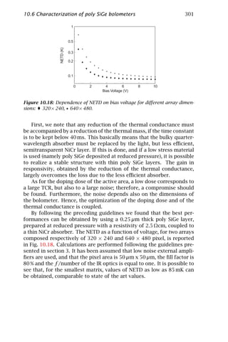
![302 10 Poly SiGe Bolometers
10.7 Conclusions
In this work, a brief survey of thermal imagers has been presented. It
has been shown that microbolometers can provide a cheap detector
technology for high performance uncooled FPAs. The different materi-
als used for microbolometers have been mentioned, and the advantages
of using poly SiGe have been highlighted. It has been shown that poly
SiGe can be processed in a standard way without requiring ad hoc op-
timized processes. Furthermore, it is compatible with standard IC pro-
cesses and, thus, it can be easily integrated with the driving electronics.
This feature improves the fill factor of the pixels and reduces the cost
of the FPA as it can be fabricated with standard foundry facilities and
does not need a special setup.
Results achieved to date are very promising in terms of thermal in-
sulation (close to 10−7 W/K), TCR (between (−1 % and −2 %) and IR emis-
sivity (an average of 90 % over the wavelength range 8–12 µm). Respon-
sivities in excess of 105 V/W have been demonstrated. The measured
1/f noise is somewhat large and is, at the moment, the most serious
impediment in achieving outstanding results. Based on the physical
properties of poly SiGe and on the performance of the already realized
detectors, the NETD of a focal plane array comprising of 320 × 240
pixels, has been computed. A value of 85 mK has been found. This
value is close to the best one reported for focal plane arrays based on
vanadium oxide [66], and smaller than values obtained with metals (90
mK, 128 × 128 pixels [40]) and with amorphous semiconductors (100
mK, 256 × 64 pixels [68]).
We want to stress that these results are based on our actual knowl-
edge of the properties of poly SiGe and there is still room for improve-
ment. The most important point is to control the 1/f noise, without
being obliged to use a high doping dose, which also implies a low TCR.
We have seen that noise and strain depend on the deposition pressure,
but, more generally, they depend on the deposition conditions. An op-
timization in this direction is now under development. To clarify this
issue, we mention that an accurate choice of the deposition conditions
of the material prepared at reduced pressure could bring its noise level
to the one typical of atmospheric pressure material. In this way a de-
crease of the NETD by a factor of 2 will be readily obtained. We also
note that 1/f noise in polycrystalline layers can be reduced by laser
recrystallization, as observed in thin film transistors [69]. The use of
this technique to reduce the 1/f noise in poly SiGe bolometers will also
be explored in the near future. After optimizing the 1/f noise, the next
step will be the realization of poly SiGe FPAs.](https://image.slidesharecdn.com/computervision-handbookofcomputervisionandapplicationsvolume1-sensorsandimaging-120205081125-phpapp02/85/Computer-vision-handbook-of-computer-vision-and-applications-volume-1-sensors-and-imaging-327-320.jpg)
![10.8 References 303
10.8 References
[1] Hudson, R. and Hudson, J., (1975). The military applications of remote
sensing by infrared. Proc. IEEE, 63:104–128.
[2] Ichikawa, M., (1989). Infrared spectra of penetration depth of into water
and water refraction-index. Proc. SPIE, 1157:318–328.
[3] Golay, M. J. E., (1947). A pneumatic infra-red detector. Rev. Sci., Instr., 18:
357–362.
[4] Scott Barr, E., (1962). The infrared pioneers-II. Macedonio Melloni. In-
frared physics, 2:67–73.
[5] Putley, E. H., (1964). The ultimate sensitivity of sub-mm detectors. In-
frared Physics, 4:1–8.
[6] Putley, E. H., (1977). Semiconductors and semi metals. In Willardson, R. K.
and Beer, A. C. (eds.), Infrared Detectors, Vol. 2. New York: Academic
Press.
[7] Abedini, Y. S., Barrett, O. R., Kim, J. S., Wen, D. D., and Yeung, S. S., (1996).
656 × 492-element platinum silicide infrared charge-coupled-device focal
plane array. Proc. SPIE, 2020:36–40.
[8] Wilson, T. E., Henricks, T. F., Halvis, J., Rosner, B. D., and Shiskowski, R. R.,
(1992). Versatile multimode 320 × 240/256 × 256 hybrid InSb infrared
focal plane array with selectable snapshot or rolling integration. Proc.
SPIE, 1762:401–406.
[9] Kanno, T., Saga, M., Kawahara, A., Oikawa, R., Ajisawa, A., Tomioka, Y.,
Oda, N., Yamagata, T., Murashima, S., Shima, T., and Yasuda, N., (1993).
Development of MBE-grown HgCdTe 64 × 64 FPA for long-wavelength IR
detection. Proc. SPIE, 2020:41–48.
[10] Wenger, L. and Gaalema, S., (1992). Low power multiplexed lead salt ar-
rays. Proc. SPIE, 1762:407–417.
[11] Sedky, S., Fiorini, P., Caymax, M., Verbist, A., and Baert, C., (1998). IR
bolometers made of polycrystalline silicon germanium. Sensors and Ac-
tuators A, 66 (1-3):193–199.
[12] Flanney, R. E. and Miller, J. E., (1992). Status of uncooled infrared imagers.
Proc. SPIE, 1689:379–395.
[13] Hanson, C., (1993). Uncooled thermal imaging at Texas Instruments. Proc.
SPIE, 2020:330–339.
[14] Horn, S. and Buser, R., (1993). Uncooled sensor technology. Proc. SPIE,
2020:304–321.
[15] Owen, R., Belcher, J., Beratan, H., and Frank, S., (1994). Producability
advances in hybrid uncooled infrared devices. Proc. SPIE, 2225:79.
[16] Owen, R., Frank, S., and Daz, C., (1992). Producibility of uncooled IR FRA
detectors. Proc. SPIE, 1683:74.
[17] Watton, R., Denims, P. N. J., Gillhan, J. P., Manning, P. A., Perkins, M. C. J.,
and Todd, M. A., (1993). IR bolometer arrays, the route to uncooled,
affordable thermal imaging. Proc. SPIE, 2020:379–390.
[18] Wood, R. A., (1993). Uncooled thermal imaging with monolithic silicon
focal plane. Proc. SPIE, 2020:322–329.](https://image.slidesharecdn.com/computervision-handbookofcomputervisionandapplicationsvolume1-sensorsandimaging-120205081125-phpapp02/85/Computer-vision-handbook-of-computer-vision-and-applications-volume-1-sensors-and-imaging-328-320.jpg)
![304 10 Poly SiGe Bolometers
[19] Liddiard, K. C., (1984). Thin-film resistance bolometer IR detectors. In-
frared Phys., 24:57–64.
[20] Liddiard, K. C., (1986). Thin-film resistor bolometer IR detectors II. In-
frared Phys., 26:43–49.
[21] Liddiard, K. C., (1993). Thin-film monolithic detector arrays for uncooled
thermal imaging. Proc. SPIE, 1969:206–216.
[22] Liddiard, K. C., Ringh, U., and Jansson, C., (1995). Staring focal plane
arrays for advanced ambient temperature infrared sensor. Proc. SPIE,
2552:564–572.
[23] Liddiard, K. C., Unewisse, M. H., and Reinhold, O., (1994). Design and fab-
rication of thin-film monolithic uncooled infrared detector arrays. Proc.
SPIE, 2225:62–71.
[24] Unewisse, M. H., Liddiard, K. C., and et al., B. I. C., (1995). Semiconductor
film bolometer technology for uncooled IR sensor. Proc. SPIE, 2552:77–87.
[25] Richards, P. L., (1994). Bolometers for infrared and millimeter waves. J.
Appl. Phys., 76(1):1–24.
[26] Kamins, T. L., (1988). Polycrystalline Silicon for Integrated Circuit Appli-
cations. Boston: Kluwer.
[27] Smith, R. A., Jones, F. E., and Chasmar, R. P., (1968). The Detection and
Measurement of Infra-Red Radiation, 2nd edition. London: Oxford Uni-
versity Press.
[28] Laker, K. R. and Sansen, W. M. C., (1994). Design of Analog Integrated
Circuits and Systems. New York: McGraw-Hill.
[29] Hooge, F. N., (1969). 1/f noise is no surface effect. Physics Letter A, 29:
139.
[30] Gallo, M. A., Willits, D. S., Lubke, R. A., and Thiede, E. C., (1993). Low cost
uncooled IR sensor for battlefield surveillance. Proc. SPIE, 2020:351–362.
[31] Watton, R., Manning, P. A., Perkins, M., Gillham, J., and Todd, M., (1996).
Uncooled IR imaging: Hybrid and integrated bolometer arrays. Proc. SPIE,
2744:486–499.
[32] Herring, R. J. and Howard, P. E., (1996). Design and performance of the
ULTRA 320 × 240 uncooled focal plane array and sensor. Proc. SPIE, 2746:
2–12.
[33] Meyer, B., Cannata, R., Stout, A., Gim, A., Taylor, P., Woodbury, E.,
Deffner, J., and Ennerson, F., (1996). Amber’s uncooled microbolometer
LWIR camera. Proc. SPIE, 2746:13–22.
[34] Marshall, C., Butler, N., Blackwell, R., Murphy, R., and Breen, I. T., (1996).
Uncooled infrared sensor with digital focal plane array. Proc. SPIE, 2746:
23–31.
[35] Marasco, P. L. and Dereniak, E. L., (1993). Uncooled infrared sensor per-
formance. Proc. SPIE, 2020:363–378.
[36] Lang, W., Steiner, P., Schaber, U., and Richter, A., (1994). A thin film
bolometer using porous silicon technology. Sensors and Actuators A, 43:
185–187.](https://image.slidesharecdn.com/computervision-handbookofcomputervisionandapplicationsvolume1-sensorsandimaging-120205081125-phpapp02/85/Computer-vision-handbook-of-computer-vision-and-applications-volume-1-sensors-and-imaging-329-320.jpg)
![10.8 References 305
[37] Shie, J. S., Chen, Y. M., and Chou, B. C. S., (1996). Characterization and
modeling of metal film microbolometer. Jour. Microelectromechanical
Systems, 5 (4):298–305.
[38] Shie, J. S. and Wenig, P. K., (1992). Design considerations of metal-film
bolometer with micromachined floating membrane. Sensors and Actua-
tors A, 33:183–189.
[39] Tanaka, A., Matsumoto, S., Tsukamoto, N., Itoh, S., Endoh, T., Nakazato, A.,
Kumazawa, Y., Himikawa, M., Gotoh, H., Tomaka, T., and Teranishi, N.,
(1995). Silicon IC process compatible bolometer infrared focal plane ar-
ray. In The 8th International Conference on Solid State Sensors and Ac-
tuators and Eurosensors IX, Stockholm, Sweden, June 1995, Vol. 2, pp.
632–635. IVA, Royal Swedish Academy of Engineering Sciences.
[40] Tanaka, A., Matsumoto, S., Tsukamoto, N., Itoh, S., Chiba, K., Endoh, T.,
Nakazato, A., Okayama, K., Kumazawa, Y., Hijikawa, M., Gotoh, H.,
Tanaka, T., and Teranishi, N., (1996). Infrared focal plane array incor-
porating silicon IC process compatible bolometer. IEEE Trans. Electron
Devices, 43(11):1844–1850.
[41] Cole, B., Horning, R., Johnson, B., Nguyen, K., Kruse, P. W., and Foote, M. C.,
(1995). High performance infra red detector arrays using thin film mi-
crostructures. In Proc. IEEE Int. Symp. on Applications of Ferroelectrics,
pp. 653–656.
[42] Umadevi, P., Negendra, C. L., and Thutupalli, G. K. M., (1993). Structural,
electrical and infrared optical properties of vanadium pentoxide (V2 O5 )
thick film thermisters. Sensors and Actuators A, 39:59–69.
[43] Parker, T. W., Marshall, C. A., Kohin, M., and Murphy, R., (1997). Uncooled
infrared sensors for surveillance and law enforcement applications. Proc.
SPIE, 2935:182–187.
[44] Butler, N., Blackwell, R., and et al., R. M., (1995). Low-cost uncooled mi-
crobolometer imaging system for dual use. Proc. SPIE, 2552:583.
[45] Chudnovskii, F. A., (1975). Metal-semiconductor phase transition in vana-
dium oxides and its technical applications. Sov. Phys. Tech. Phys., 20:999.
[46] Jerominek, H., Picard, F., and Vicent, D., (1993). Vanadium oxide films for
optimal switching and detection. Opt. Eng., 32:2092–2099.
[47] Kuznetsov, V. A. and Haneman, D., (1997). High temperature coefficient
of resistance in vanadium oxide diodes. Rev. Sci. Instrum., 68 (3):1518–
1520.
[48] Umadevi, P., Negendra, C. L., and et al., G. K. M. T., (1991). A new thermis-
tor material for thermistor bolometer: Material preparation and charac-
terization. Proc. SPIE, 1485:195.
[49] Zerov, V. Y., Kulikov, Y. V., Malyarov, V. G., Feokistov, N. A., and
Kherbtov, I. A., (1997). Bolometric properties of silicon thin-film struc-
tures fabricated by plasmochemical vapor-phase deposition. Tech. Phys.
Lett., 23 (6):481–483.
[50] Enukova, T. A., Ivanova, N. L., Kulikov, Y. V., Malyarov, V. G., and
Khrebtov, I. A., (1997). Amorphous silicon and germanium films for un-
cooled microbolometers. Tech. Phys. Lett., 23(7):504–506.](https://image.slidesharecdn.com/computervision-handbookofcomputervisionandapplicationsvolume1-sensorsandimaging-120205081125-phpapp02/85/Computer-vision-handbook-of-computer-vision-and-applications-volume-1-sensors-and-imaging-330-320.jpg)
![306 10 Poly SiGe Bolometers
[51] Ichihara, T., Watabe, Y., Honda, Y., and Aizawa, K., (1997). A high perfor-
mance amorphous Si1−x Cx :H thermister bolometer based on microma-
chined structure. In 1997 International Conference on Solid State Sensors
and Actuators, Chicago, pp. 1253–1256.
[52] NMRC, (1995). The development of integrated micro-bolometer arrays. In
Scientific Report’95, p. 11. National Microelectronics Research Center.
[53] Paul, O., Korviet, J., and Boltes, H., (1994). Determination of the thermal
conductivity of CMOS IC polysilicon. Sensors and Actuators A, 41-42:
161–164.
[54] Maier-Schneider, D., Maibach, J., Obermeier, E., and Schneider, D., (1995).
Variation in young’s modulus and intrinsic stress of LPCVD-polysilicon
due to high temperature annealing. J. Micromech. Microeng., 5:121–124.
[55] Vining, C. B., (1991). A model for the high temperature transport proper-
ties of heavily doped n-type silicon-germanium alloys. J. Appl. Phys., 69:
331–341.
[56] Steigmeier, E. F. and Abeles, B., (1964). Scattering of phonons by electrons
in germanium-silicon alloys. Phys. Rev., 136:A1149.
[57] Slack, G. A. and Hussain, M. A., (1991). The maximum possible conversion
efficiency of silicon germanium thermoelectric generators. J. Appl. Phys.,
70:2694–2718.
[58] Dismukes, J., Ekstrom, L., Steigmeier, E., Kudam, I., and Beers, D., (1964).
Thermal and electrical properties of heavily doped Ge-Si alloys up to
1300 °C. J. Appl. Phys., 35:2899.
[59] Fiorini, P., Sedky, S., Caymax, M., and Baert, K., (1997). Preparation and
residual stress characterization of poly-silicon germanium films prepared
by atmospheric pressure chemical vapor deposition. Proc. Mat. Res. Soc.
Symp., 472:227–231.
[60] Core, T. A., Tsang, W. K., and Sherman, S. J., (1993). Fabrication technology
for an integrated surface micromachined sensor. Solid State Technology,
36:39–48.
[61] Tas, N., Sonnenberg, T., Jansen, H., Legtenberg, R., and Spoek, M. E., (1996).
Stiction in surface micromachining. J. Micromech. Microeng., 6:385–397.
[62] Strimer, P., Gerbaux, X., Hadni, A., and Souel, T., (1981). Black coatings
for infrared and visible, with high electrical resistivity. Infra Red Physics,
21:37–39.
[63] Betts, D. B., Clarke, F. J. J., Cox, L. J., and Larkin, J. A., (1985). Infrared
reflection properties of five types of black coating for radiometric detec-
tors. J. Physics, 18:689–696.
[64] Veremei, V. V. and Pankrotov, N. A., (1974). Interference phenomena in
semiconductor bolometers. Sov. J. Opt. Technol., 41:199.
[65] Parsons, A. D. and Pedder, D. J., (1988). Thin-film infrared absorber struc-
tures for advanced thermal detectors. J. Vac. Sci. Technol., A6 (3):1686–
1689.
[66] Stout, A. and Rittenberg, E., (1997). High performance hand-held thermal
imager for law enforcement. Proc. SPIE, 2935:154–157.](https://image.slidesharecdn.com/computervision-handbookofcomputervisionandapplicationsvolume1-sensorsandimaging-120205081125-phpapp02/85/Computer-vision-handbook-of-computer-vision-and-applications-volume-1-sensors-and-imaging-331-320.jpg)
![10.8 References 307
[67] Pankratov, N. A. and Malyarov, N. G., (1985). Detector layout of a submil-
limeter photometer. Zh. Prikl. Specktrosk., 42:1028.
[68] Tissot, J. L., (1998). What is an uncooled infrared microbolometer?
(French). CLEFS CEA, 37:28–33.
[69] Carluccio, R., Corradetti, A., Fortunatto, G., Reita, C., Legagneux, P.,
Plais, F., and Pribat, D., (1997). Noise performances in polycrystalline
silicon thin-film transistors fabricated by excimer laser crystallization.
Appl. Phys. Lett., 71:578–580.](https://image.slidesharecdn.com/computervision-handbookofcomputervisionandapplicationsvolume1-sensorsandimaging-120205081125-phpapp02/85/Computer-vision-handbook-of-computer-vision-and-applications-volume-1-sensors-and-imaging-332-320.jpg)


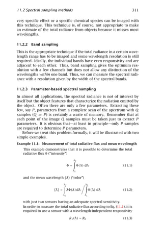

![11.2 Spectral sampling methods 313
It is important to note that both line and band sampling are not suit-
able to determine the mean wavelength and total radiant flux. Sam-
pling just at two lines misses all wavelengths except the two selected
lines. Thus the total radiant flux is incorrect.
With band sampling it is possible to get the total radiant flux right
provided that the two selected bands are adjacent to each other and
cover the whole wavelength range of interest. The mean wavelength,
however, comes out incorrectly in the general case. This is directly
related to the fact that within the selected band all wavelengths are
equally weighted. The wavelength of a monochromatic radiative flux,
for example, cannot be determined with better resolution than the
bandwidth of the individual channels. What is needed according to
Eq. (11.4) is linearly changing responsivity over the wavelength inter-
val for the second sensor.
The example also illustrates that measurements of this type are always
a many-to-one mapping. The two sensors receive the same signal for
all types of spectral distributions that have the same total radiant flux
and mean wavelength as defined by Eqs. (11.1) and (11.2).
Example 11.2: Measurement of total radiative flux, mean, and variance of
the wavelength
The two-channel system discussed in Example 11.1 cannot measure
the width of a spectral distribution at all. This deficit can be over-
come with a third channel that has a sensitivity that increases with
the square of the distance from the mean wavelength (Fig. 11.1b).
The responsivity of the third sensor is given by
˜
R3 (λ) = 4λ2 R0 (11.9)
Consequently, the mean squared wavelength is given by
˜ 1 s3
λ2 = (11.10)
4 s1
2 2
2
The variance σλ = ˜ ˜
λ− λ ˜ ˜
= λ2 − λ is then given by
˜
2
2 1 s3 s2 1
σλ =
˜ − − (11.11)
4 s1 s1 2
For a monochromatic distribution at the wavelength λ0 the variance
is zero. Then
2
σλ = λ2 − λ0
2
˜ 0 = λ2 − λ2 = 0
0 0 (11.12)
The estimates given by Eqs. (11.10) and (11.11) are only valid as long
as the spectral distribution is confined to the interval [λ1 , λ2 ] to which
the sensors respond.](https://image.slidesharecdn.com/computervision-handbookofcomputervisionandapplicationsvolume1-sensorsandimaging-120205081125-phpapp02/85/Computer-vision-handbook-of-computer-vision-and-applications-volume-1-sensors-and-imaging-338-320.jpg)
![314 11 Hyperspectral and Color Imaging
After these two introductory examples, we formulate linear param-
eter-based sampling in a general way as a linear discrete inverse problem
[1]. As in Examples 11.1 and 11.2 we assume that P parameters p of
interest are a linear combination of the spectral flux density and we
want to measure them from other linear combinations of the spectral
flux density by the use of Q sensor signals q with various spectral
sensitivities. The general question is whether this is possible at all in
general and if yes under which conditions.
In order to derive the relation between the parameters p and the
sensor signals q, we assume a hypothetical band-sampled spectral den-
sity s with S samples. The sampling must be dense enough so that the
sampling theorem (see Volume 2, Section 2.4.2) is met. Then the linear
relations between the band-sampled spectral density s and the param-
eter vector p and the signal vector q can be written as:
p = Ps and q = Qs (11.13)
where P and Q are P × S and Q × S matrices, respectively, with P ≤ Q ≤ S.
Given the linear nature of the ansatz, the direct relation between p and
q must also be linear provided that a solution exists at all:
p = Mq (11.14)
Replacing q in Eq. (11.14) by q = Qs and using p = Ps, a direct relation
between the three matrices M, P, and Q is obtained:
P = MQ (11.15)
Using standard least-squares techniques (see, e. g., Menke [1]), the P × Q
matrix M is given by
M = PP T PQT (QP T PQT )−1 (11.16)
provided that the inverse of the Q × Q matrix QP T PQT exists. Thus
this equation tells us both the condition for the existence of a solution
and how to compute it by matrix-matrix multiplications. The solubility
does not depend at all on the actual measurements q but only on the
spectral responsitivity of the Q sensors Q and the spectral shape of
the parameters p to be estimated that are contained in the matrix P.
With this general formulation we have a powerful general concept.
We can use it to handle any multispectral or multichannel image pro-
cessing task where we measure Q channels and want to retrieve P pa-
rameters that are linear combinations of the measured signals. The
two simple Examples 11.1 and 11.2 discussed at the beginning of this
section, human color vision (see Section 11.3), and differential optical
absorption spectroscopy (DOAS) discussed in Volume 3, Chapter 37 are
just four examples of this general type of problems.](https://image.slidesharecdn.com/computervision-handbookofcomputervisionandapplicationsvolume1-sensorsandimaging-120205081125-phpapp02/85/Computer-vision-handbook-of-computer-vision-and-applications-volume-1-sensors-and-imaging-339-320.jpg)
![11.3 Human color vision 315
1
0.8
0.6
0.4
0.2
λ[nm]
0
400 450 500 550 600 650 700
Figure 11.2: Estimates of the relative cone sensitivities of the human eye after
DeMarco et al. [2].
11.3 Human color vision
Human color vision can be regarded in terms of the spectral sampling
techniques summarized in Table 11.1 as a parameter-based sampling.
It does not measure the spectral radiant flux directly but rather proper-
ties of the spectral distribution such as the total radiant flux (intensity),
the mean wavelength (color ), and the width of the spectral distribution
(saturation of the color). If the width of the spectral distribution is nar-
row we have a pure color with high saturation. If the spectral distribu-
tion is wide, the color has a low saturation. If the spectral distribution
is flat, we sense no color. With the respect to this discussion, it appears
that the three-sensor system discussed in Example 11.2 appears to be
an ideal intensity-color-saturation sensor. It is ideal in the sense that it
has a linear response and the wavelength (color) and width (saturation)
resolution are independent of the wavelength. Thus it is interesting to
compare this three-sensor system with the color-sensing system of the
human eye.
For color sensing, the human eye has also three types of photopig-
ments in the photoreceptors known as cones with different spectral
sensitivities (Fig. 11.2). The sensitivities cover different bands with
maximal sensitivities at 445 nm, 535 nm, and 575 nm, respectively (band
sampling), but overlap each other significantly (parameter-based sam-
pling). In contrast to our model examples, the three sensor channels
are unequally spaced and cannot simply be linearly related. Indeed, the
color sensitivity of the human eye is uneven and all the nonlinearities
involved make the science of color vision rather difficult. Here, only
some basic facts are given—in as much as they are useful to handle
color imagery.](https://image.slidesharecdn.com/computervision-handbookofcomputervisionandapplicationsvolume1-sensorsandimaging-120205081125-phpapp02/85/Computer-vision-handbook-of-computer-vision-and-applications-volume-1-sensors-and-imaging-340-320.jpg)
![316 11 Hyperspectral and Color Imaging
11.3.1 Three-dimensional color space
Having three color sensors, it is obvious that color signals cover a 3-D
space. Each point in this space represents one color. From the discus-
sion on spectral sampling in Section 11.2, it is clear that many spectral
distributions called metameric color stimuli or short metameres map
onto one point in this space. Generally, we can write the signal si re-
ceived by a sensor with a spectral responsivity Ri (λ) as
si = Ri (λ)Φ(λ)dλ (11.17)
With three primary color sensors, a triple of values is received, often
called tristimulus and represented by the 3-D vector s = [s1 , s2 , s3 ]T .
11.3.2 Primary colors
One of the most important questions in colorimetry is a system of how
to represent colors as linear combinations of some basic or primary
colors. A set of three spectral distributions Φj (λ) represents a set of
primary colors and results in an array of responses that can be de-
scribed by the matrix P with
Pij = Ri (λ)Φj (λ)dλ (11.18)
T
Each vector p j = p1j , p2j , p3j represents the tristimulus of the
primary colors in the 3-D color space. Then, it is obvious that any color
can be represented by the primary colors that are a linear combination
of the base vectors p j in the following form:
s = Rp 1 + Gp 2 + Bp 3 with 0 ≤ R, G, B ≤ 1 (11.19)
where the coefficients are denoted by R, G, and B, indicating the three
primary colors red, green, and blue. Note that these coefficients must
be positive and smaller than one. Because of this condition, all colors
can be presented as a linear combination of a set of primary colors only
if the three base vectors are orthogonal to each other. This cannot be
the case as soon as more than one of the color sensors responds to one
primary color. Given the significant overlap in the spectral response of
the three types of cones (Fig. 11.2), it is obvious that none of the color
systems based on any type of real primary colors will be orthogonal.
The colors that can be represented lie within the parallelepiped formed
by the three base vectors of the primary colors. The more the primary
colors are correlated with each other (i. e., the smaller the angle between
two of them is), the smaller is the color space that can be represented](https://image.slidesharecdn.com/computervision-handbookofcomputervisionandapplicationsvolume1-sensorsandimaging-120205081125-phpapp02/85/Computer-vision-handbook-of-computer-vision-and-applications-volume-1-sensors-and-imaging-341-320.jpg)
![11.3 Human color vision 317
Table 11.2: Most often used primary color systems. The second column gives
also the conversion matrix of the corresponding color system to the XY Z color
system (values taken from Wendland [3, Section 5.7.4] and Pratt [5, Table 3.5-1]).
Name Description
Monochromatic primaries Adapted by C.I.E. in 1931
Rc , Gc , Bc λ
R = 700 nm, λG = 546.1 nm, λB = 435.8 nm
0.490 0.310 0.200
0.177 0.812 0.011
0.000 0.010 0.990
NTSC Primary Receiver FCC Standard, 1954, to match phosphors of
Standard RN , GN , BN RGB color monitors
0.6070 0.1734 0.2006
0.2990 0.5864 0.1146
0.0000 0.0661 1.1175
S.M.P.T.E. Primary Receiver Better adapted to modern screen phosphors
Standard RS , GS , BS 0.393 0.365 0.192
0.212 0.701 0.087
0.019 0.112 0.985
EBU Primary Receiver Stan- Adopted by EBU 1974
dard Re , Ge , Be 0.4303 0.3416 0.1780
0.2219 0.7068 0.0713
0.0202 0.1296 0.9387
by them. Mathematically, colors that cannot be represented by a set of
primary colors have at least one negative coefficient in Eq. (11.19). The
most often used primary color systems are summarized in Table 11.2.
11.3.3 Chromaticity
One component in the 3-D color space is intensity. If a color vector is
multiplied by a scalar, only its intensity is changed but not its color.
Thus, all colors could be normalized by the intensity. This operation
reduces the 3-D color space to a 2-D color plane or chromaticity dia-
gram:
R G B
r= , g= , b= (11.20)
R+G+B R+G+B R+G+B
with
r +g+b =1 (11.21)
It is sufficient to use only the two components r and g. The third
component is then given by b = 1 − r − g, according to Eq. (11.21).](https://image.slidesharecdn.com/computervision-handbookofcomputervisionandapplicationsvolume1-sensorsandimaging-120205081125-phpapp02/85/Computer-vision-handbook-of-computer-vision-and-applications-volume-1-sensors-and-imaging-342-320.jpg)
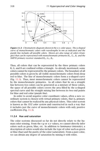

![320 11 Hyperspectral and Color Imaging
tee on Colorimetry of the Optical Society of America [4]. An excellent
treatment of color with respect to digital image processing is given by
Pratt [5] and with respect to video engineering by Inglis [6].
11.3.5 Intensity-hue-saturation color coordinate system
Here, we discuss only one further color coordinate system that is opti-
mally suited to present vectorial image information as colors on moni-
tors. With a gray scale image, only one parameter can be represented. In
color, it is, however, possible to represent three parameters simultane-
ously, for instance as intensity, hue, and saturation (IHS). This represen-
tation is known as the IHS color coordinate system. The transformation
is given by
I 1/3 1/3 1/3 R
U = 2/3 −1/3 −1/3 G
V −1/3 2/3 −1/3 B
(11.22)
V
H = arctan
U
S = (U 2 + V 2 )1/2
This transformation essentially means that the zero point in the
chromaticity diagram has been shifted to the white point. The pairs
[U , V ]T and [S, H]T are the Cartesian and polar coordinates in this new
coordinate system, respectively.
11.4 References
[1] Menke, W., (1984). Geophysical data analysis: discrete inverse theory. Or-
lando: Academic Press.
[2] DeMarco, P., Pokorny, J., and Smith, V. C., (1992). Full-spectrum cone sen-
sitivity functions for X-chromosome-linked anomalous trichromats. J. Op-
tical Society, A9:1465–1476.
[3] Wendland, B., (1988). Fernsehtechnik I: Grundlagen. Heidelberg: Hüthig.
[4] Committee on Colorimetry, Optical Society of America, (1953). The Science
of Color. Washington, D. C.: Optical Society of America.
[5] Pratt, W., (1991). Digital image processing. New York: Wiley.
[6] Inglis, A. F., (1993). Video engineering. New York: McGraw-Hill.](https://image.slidesharecdn.com/computervision-handbookofcomputervisionandapplicationsvolume1-sensorsandimaging-120205081125-phpapp02/85/Computer-vision-handbook-of-computer-vision-and-applications-volume-1-sensors-and-imaging-345-320.jpg)


![324 12 Dynamic Fluorescence Imaging
from such diverse fields as environmental physics (Volume 3, Chap-
ter 33) to the broad range of life sciences including molecular biology,
DNA-sequencing, neurobiology and biophysical studies of functional
mechanisms in living cells. As living cells are highly compartimen-
talized on a nano- to micrometer scale and respond to environmen-
tal changes on a millisecond time scale, many of their properties can
only be studied with a comprehensive approach to dynamic fluores-
cence imaging. With biological cellular preparations as examples, the
present chapter discusses the most important properties of selected
fluorescent indicators, microscopic techniques and essential steps for
the required mathematical image analysis.
Particular emphasis is given to the use of fluorescence imaging tech-
niques in the determination of intracellular ion concentrations in living
cells under in vivo and in vitro conditions. For this application fluores-
cence techniques are the most popular tools. In addition to the high
spatial and temporal resolution fluorescence imaging offers, sensitivity
and selectivity for specific ions are among the largest benefits. Further-
more, the possibility of spectroscopic analysis allows direct informa-
tion to be obtained about the molecules and the interaction with their
environment. First, we want to give a brief account of the nature of
fluorescence and its molecular origin.
12.2 Fluorescence
Fluorescence has been used by physicists and biochemists since the
1920s. Many biochemical intermediates are naturally fluorescent, for
example, the enzyme cofactor NADH involves a drop in the fluorescence
emission when oxidized to NAD+ , which can be used as a sensitive
indicator for cellular metabolism [1].
Today, there is a rapid increase in fluorescence techniques in cellu-
lar biology, especially in monitoring intracellular signaling pathways.
For example, the development of the ratiometric dyes by Prof. Roger
Y. Tsien’s group in the mid-1980s [2] has led to enormous progress
in the accurate determination of intracellular calcium concentrations.
Recently, the so-called green fluorescent protein (GFP), produced in chi-
meric target constructs with an attached fluorophore, extended as a
very specific marker for genetic expression even further the use of fluo-
rescent techniques in cell biology and molecular physiology [3].
12.2.1 Physical properties of fluorescence
Fluorescence is the result of a quantum mechanically “allowed” transi-
tion of electrons in certain molecules typically called fluorophores or
fluorescent dyes from an excited state to the ground state. The energy](https://image.slidesharecdn.com/computervision-handbookofcomputervisionandapplicationsvolume1-sensorsandimaging-120205081125-phpapp02/85/Computer-vision-handbook-of-computer-vision-and-applications-volume-1-sensors-and-imaging-349-320.jpg)
![12.2 Fluorescence 325
for the excitation of the dye is mostly supplied as photons by an excita-
tion light source as, for example, high-pressure arc lamps or lasers. The
typical fluorescence lifetimes, that is, the average time the fluorophore
stays in the excited state, range from 10−9 s to 10−7 s . Following light
absorption, several processes occur (see [4]). A fluorophore is usually
excited to some higher vibrational level of either S1 ,S2 , or S3 , as shown
in Fig. 12.1, where Si denotes the different electronic singlet states of
the fluorophore. Mostly relaxation to the lowest vibrational level of S1
occurs in the order of 10−12 s. This so-called internal conversion is ba-
sically a transfer of energy to the surrounding medium as heat. From
this state, either fluorescence emission or radiationless decay to one
of the vibrational states of S0 occurs. The emission of fluorophores
generally occurs at wavelengths longer than those of absorption. This
“Stokes shift ” is a result of several processes, including internal con-
version of excited states to the lowest vibrational level of S1 or solvent
relaxation effects as shown in Fig. 12.1. The sensitivity of fluorescence
techniques is based on the fact that the emitted fluorescence photons
can be detected against a low background, separated from the excita-
tion photons by the Stokes shift.
The energy for the excitation of the fluorophore can either origi-
nate from the absorption of a single photon with energy hνa , where
h is Planck’s constant and ν is the frequency of the light, or from the
absorption of either two photons with energy hνa /2 or from multiple
photon absorption. The absorption of two or more photons is used in
nonlinear scanning microscopy and will be described in Section 12.4.4.
The absorption probability for a single photon is linearly proportional
to the initial excitation light intensity, whereas there is a quadratic de-
pendence for the two-photon absorption process.
From the law of Lambert-Beer that states that the extinction for one
photon absorption is proportional to the concentration of the absorb-
ing species and to the optical path length, it can be derived that under
the assumption of a dilute solution the fluorescence intensity If is pro-
portional to the concentration c of the absorbing substance
If ∝ (λ)cxI0 q (12.1)
where (λ) is the wavelength-dependent extinction coefficient, x is the
thickness of the sample volume, and I0 is the excitation light intensity.
The quantum yield q is defined as the ratio of fluorescence photons to
the number of photons absorbed. Neglecting intersystem crossings in
Fig. 12.1, the quantum yield can be written approximately as
σ
q= (12.2)
σ +k](https://image.slidesharecdn.com/computervision-handbookofcomputervisionandapplicationsvolume1-sensorsandimaging-120205081125-phpapp02/85/Computer-vision-handbook-of-computer-vision-and-applications-volume-1-sensors-and-imaging-350-320.jpg)
![326 12 Dynamic Fluorescence Imaging
S 4
S 3
S 2
in te r n a l c o n v e r s io n
( 1 0 -1 2 s )
S 1 s o lv e n t r e la x a tio n
( 1 0 -1 1 s )
S 1 '
r a d ia tio n le s s
d e c a y
a b s o r p tio n (k )
h ∗ ν( 1 0 - 1 5 s )
a
flu o r e s c e n c e
h ∗ ν( 1 0 - 8 s )
f
(σ )
S 0
Figure 12.1: Typical energy levels and time scales of transitions for a fluo-
rophore. The ground, first and second electronic states are depicted by S0, S1
and S2 further divided into various vibrational and rotational states that are
omitted for simplicity; S1 is the lowered S1 state due to solvent relaxation. The
rate of fluorescence emission is denoted by σ and the rate of all possible radia-
tionless decay processes by k. Possible intersystem crossings from the S1 singlet
state to the first triplet state T1 , which result in phosphorescence emission, are
neglected. Adopted from [4].
where σ denotes the rate of fluorescence emission and k denotes the
rate of all possible radiationless decay processes.
If the fluorescence spectrum is different for the free and the bound
form of the fluorescent dye the amount of ions complexed by the dye
can be determined. The free ion-concentration can be subsequently
obtained with the knowledge of the dissociation constant Kd of the
dye-ion complexation reaction.
It is important to note that the fluorescence intensities are propor-
tional to the concentration over only a limited range of concentrations
of the fluorescent specimen; for larger concentrations the relation be-
comes nonlinear. Additionally, there are several attenuation effects,
which largely decrease the observed fluorescence. When the fluores-
cence emission passes through the solution, it can be reabsorbed lead-
ing to a decrease in fluorescence intensity. This loss is called the inner
filter effect and the attenuation of fluorescence emission increases with
increasing concentrations and increasing thickness of the sample vol-
ume.](https://image.slidesharecdn.com/computervision-handbookofcomputervisionandapplicationsvolume1-sensorsandimaging-120205081125-phpapp02/85/Computer-vision-handbook-of-computer-vision-and-applications-volume-1-sensors-and-imaging-351-320.jpg)
![12.2 Fluorescence 327
The sensitivity of a given fluorescent indicator not only depends on
the quantum yield defined by Eq. (12.2), but also on the absorption
characteristics of the fluorophore. The sensitivity S can be defined as
S = (λ)I0 q (12.3)
and is an important parameter, for example, in choosing the optimum
excitation wavelength, particularly when the main excitation band can-
not be used due to technical limitations of the excitation light source.
Fluorescence quenching generally refers to bimolecular processes,
which reduce fluorescence emission by inducing the relaxation of ex-
cited fluorophore molecules back into the ground state without the
emission of a fluorescence photon. This includes self- or concentration-
quenching, where one fluorophore is quenched by another, and colli-
sional quenching, which is due to transient excited state interactions.
The quenching effects include specific interactions with the solvent,
which lead to a decrease in fluorescence intensity, or interactions with
other substances present in the solution. The lifetime τ0 of an excited
state of a fluorophore without quenching is given by
1
τ0 = (12.4)
σ +k
and in the presence of a quenching substance with concentration c, the
lifetime τ is given by
τ
= 1 + Kc (12.5)
τ0
where K is the so-called quenching constant.
12.2.2 The oxygen quenching method
The decrease in fluorescence due to quenching can also be used for the
quantitative determination of concentrations of substances, which act
as quenchers. A major application is the measurement of oxygen con-
centrations in aqueous solutions. Oxygen quenches almost all known
fluorophores via collisional quenching. The decrease in fluorescence
intensity is described by the Stern-Volmer equation [4]:
If 0
If (c) = (12.6)
1 + Kc
where If0 is the fluorescence intensity without quenching, K is the
quenching constant, and c is the concentration of the quenching sub-
stance.
This technique can be used in a variety of different scientific applica-
tions. In the field of life sciences it can be used to measure the oxygen](https://image.slidesharecdn.com/computervision-handbookofcomputervisionandapplicationsvolume1-sensorsandimaging-120205081125-phpapp02/85/Computer-vision-handbook-of-computer-vision-and-applications-volume-1-sensors-and-imaging-352-320.jpg)
![328 12 Dynamic Fluorescence Imaging
concentration in living cells and tissue [5]. The method is also suc-
cessfully applied in environmental physics, where concentration fields
of dissolved oxygen are measured in the boundary layer at the water
surface to study the mechanisms of air-water gas transfer [6].
12.3 Fluorescent indicators
The optical methods to quantify intracellular ion concentrations can
be discussed very well using the example of Ca2+ -sensitive techniques,
as the investigation of intracellular Ca2+ -levels has been the major ap-
plication. The three most important techniques to quantify intracellu-
lar Ca2+ -levels are measurements with photoproteins, absorption mea-
surements and fluorescence measurements (see Thomas [7]). Photopro-
teins are obtained from luminescent organs of coelenterates and emit
light when reacting with Ca2+ . This method was first used by Ridgway
and Ashley [8], who could measure intracellular Ca2+ -levels in muscle
fibers.
The development of Ca2+ -sensitive dyes (azo-dyes, namely, arse-
nazo III and antipyrylazo III) in the mid-1970s has allowed the start of
absorption measurements and has been particularly useful in studying
the fast Ca2+ -transients in skeletal muscle fibers, although the absorp-
tion changes are difficult to detect and to interpret, especially in larger
cellular preparations.
The introduction of fluorescent indicators has greatly facilitated the
measurement of intracellular ion concentrations and, combined with
the various microscopic techniques available today, they provide the
most powerful tools.
12.3.1 Calcium indicators
Many useful calcium indicators have been developed in Tsien’s lab and
are derivatives of the Ca2+ buffer BABTA, including Quin-2, Fura-2,
Indo-1, Fluo-3 and Rhod-2 (see Haugland and Minta [9]). They are chem-
ically designed fluorescent dyes having an additional Ca2+ -complexing
moiety like EDTA or EGTA. For example, Fluo-3 is obtained by using
fluorescein and EDTA.
Calcium indicators need to have high affinities, as typical Ca2+ -con-
centrations in cells are very low (from 10-100 nM at rest to 1-10 µM
during activation). Additionally, the selectivity against Mg2+ -ions has
to be very high as these ions competitively bind and are present in much
higher concentrations (about 1 mM).
Since the development of the ratiometric dyes, for example, Fura-
2 and Indo-1, it is possible, even using conventional fluorescence mi-
croscopy, to accurately determine intracellular calcium ion concentra-](https://image.slidesharecdn.com/computervision-handbookofcomputervisionandapplicationsvolume1-sensorsandimaging-120205081125-phpapp02/85/Computer-vision-handbook-of-computer-vision-and-applications-volume-1-sensors-and-imaging-353-320.jpg)
![12.3 Fluorescent indicators 329
a b
Figure 12.2: a Excitation spectrum of Fura-2. For an excitation wavelength of
340 nm, the fluorescence signal increases with increasing Ca2+ -concentration
and the opposite effect can be seen for an excitation wavelength of 380 nm. The
fluorescence signal is independent of the calcium concentration at the isosbestic
point at λ =360 nm; b emission spectrum of Fluo-3. Figure courtesy of Molecular
Probes Inc., Eugene, OR [10].
tions. In addition to higher fluorescence intensities and better calcium
selectivity, these dyes exhibit a strong shift in their excitation or emis-
sion wavelength upon binding of calcium. Fura-2 is designed to shift
its wavelength of excitation to shorter wavelengths with the binding of
Ca2+ -ions. As seen in Fig. 12.2, the excitation maximum for the free dye
is at a wavelength of about 370 nm and shifts to 340 nm with the bind-
ing of Ca2+ -ions, a much larger shift than in the emission spectrum.
This allows dual-excitation ratio measurements by sampling the fluo-
rescence intensities at two appropriate wavelengths λ1 and λ2 (mostly
340 nm/380 nm). Forming the ratio R of the fluorescence emissions If1
and If2 , the calcium concentration can be calculated according to the
equation originally derived by Grynkiewicz et al. [2]:
R − Rmin
[Ca2+ ] = Kd β (12.7)
Rmax − R
where Kd is the dissociation constant of the Fura-calcium complex; Rmin
and Rmax are the ratios of the fluorescence emission in the virtual ab-
sence or with a saturating amount of calcium; and β corresponds to the
ratio of fluorescence emission of the free dye to the calcium bound dye
measured at the second wavelength. Thus, calcium concentrations can
be calibrated independently of the dye concentration, specimen thick-
ness and illumination intensity. Fura-2 is a chemical derivative of the
calcium buffer BAPTA and the absorption maximum is in the near UV
with an extinction coefficient in the range of 2-3 × 10⁴ M−1 cm−1 . The](https://image.slidesharecdn.com/computervision-handbookofcomputervisionandapplicationsvolume1-sensorsandimaging-120205081125-phpapp02/85/Computer-vision-handbook-of-computer-vision-and-applications-volume-1-sensors-and-imaging-354-320.jpg)
![330 12 Dynamic Fluorescence Imaging
emission maximum is at a wavelength of 512 nm for the free dye and
shows a shift to a wavelength of 505 nm for the Ca2+ -complexed dye.
The apparent Kd of the Ca2+ -Fura-2 complex, is in the range of 135-
300 nM, strongly depending on the ionic strength of the solution and
several other factors, such as, for example, viscosity [11].
The nonratiometric Ca2+ -indicator Fluo-3 (see Fig. 12.2) offers some
advantages over UV-excitable indicators, such as it is excited in the vis-
ible part of the spectrum. It can be excited with the 488 nm line of an
argon-ion laser and, therefore, it is frequently used in laser scanning
microscopy. Due to the longer excitation wavelength, there is reduced
photodamage, light scatter and reduced cell autofluorescence. Unlike
Fura-2, Fluo-3 is essentially nonfluorescent unless bound to Ca2+ and
exhibits a more than 100-fold increase in fluorescence upon complex-
ation. The Kd of ∼ 400 nM allows the detection of Ca2+ -concentrations
of more than 10 µM without saturation.
A new generation of calcium indicators, known as “cameleons,” has
been recently developed by Tsien’s group based on the green fluores-
cent protein (GFP) [3]. These indicators combine the brightness of fluo-
rescent indicators with the target-ability of biosynthetic indicators and
are generated in situ by gene transfer into the cells. This can be used to
target the indicator to specific intracellular locations with more or less
molecular resolution, allowing the monitoring of Ca2+ -signals that are
extremely localized with very sharp gradients to their surrounding.
12.3.2 Other ions and membrane potential
The very fundamental process of electrical excitation in nerve and mus-
cle cells is governed by diffusion potentials due to intracellular and ex-
tracellular differences for Na+ -, K+ - Cl− - and Ca2+ -ion concentrations
and due to the regulation of membrane permeabilities for these ions.
These mechanisms also play very important functional roles in nonex-
citable cells in the human body and almost all plant and animal cells.
Therefore, a number of fluorescent probes have been developed in ad-
dition to the important Ca2+ -indicators, which are sensitive to the fore-
mentioned ions and also for the other regulating ions, namely, Mg2+ and
H+ (for review, see Mason [12]). All these optical probes can be catego-
rized based on their ion dependent excitation and emission spectra as
single wavelength, dual (wavelength-) excitation and dual (wavelength-)
emission dyes. There is still a largely untapped potential in particular
for the combination of those dyes to provide a most powerful tool us-
able with dynamic imaging to monitor fast biologically or clinically im-
portant concentration changes for several ions simultaneously to gain
insight into complex regulatory processes. Often, dynamic fluores-
cence imaging techniques are combined with high-resolution electro-
physiological experiments measuring transmembrane currents through](https://image.slidesharecdn.com/computervision-handbookofcomputervisionandapplicationsvolume1-sensorsandimaging-120205081125-phpapp02/85/Computer-vision-handbook-of-computer-vision-and-applications-volume-1-sensors-and-imaging-355-320.jpg)
![12.3 Fluorescent indicators 331
specific ion channel proteins. The electrophysiological techniques use
either intracellular microelectrodes (tip diameter<0.5 µm) or external
patch electrodes of similar size. It is very difficult to use these elec-
trodes for intracellular organelles or for spatially resolved measure-
ments. Therefore, potentiometric fluorescent probes were developed
to record in a noninvasive way the membrane potential changes with
high spatial resolution (see Loew [13], Wu and Cohen [14]). These dyes
can be divided into fast response probes, which can be used to mea-
sure membrane potential changes on the millisecond time scale, as, for
example, in cardiac cells and neurons in the central nervous system.
The slow-response dyes offer in general a much larger response than
the fast dyes, but with a slower kinetic and they are particularly useful
for nonexcitable cells and cellular organelles.
12.3.3 Dye kinetic and buffering
It should be noted that fluorescent indicators all have an intrinsic ki-
netic delay to changes in their environment. The quantitative analysis
of fluorescence changes, therefore, generally has to consider the kinetic
on- and off-rate constants s(kon , koff ) of the fluorophore-ion interac-
tion, which are related to the dissociation constant KD by the following
relation:
KD = koff /kon (12.8)
A second aspect of ion binding to a fluorophore is that thereby each
fluorescent indicator acts as an ion buffer itself. In many cases this
can result in pronounced alterations of the complex ion distribution in
cellular systems. Therefore, the buffering effects should be generally
taken into account in the quantitative analysis of fluorescence signals.
12.3.4 Photobleaching and photodamage
The irreversible destruction of fluorophores (photobleaching) is mostly
influenced by the excitation illumination intensity, but also by other ex-
perimental and surrounding environmental conditions of the dye (e.g.,
impeded diffusional exchange and compartmentalization of the dye,
pH, formation of radicals and oxidation and radical formation, etc.).
Therefore, high excitation intensities should be avoided, mainly by in-
creasing the detection sensitivity, or by detecting the fluorescence emis-
sion over the broadest possible wavelength band.
Photodamage is the result of interactions of the excitation photons
with the specimen. There are many different processes, which can re-
sult in the damage of cells, proteins or DNA (see Niemz [15] for a general
discussion of laser tissue interaction). In general, it can be stated that](https://image.slidesharecdn.com/computervision-handbookofcomputervisionandapplicationsvolume1-sensorsandimaging-120205081125-phpapp02/85/Computer-vision-handbook-of-computer-vision-and-applications-volume-1-sensors-and-imaging-356-320.jpg)
![332 12 Dynamic Fluorescence Imaging
photodamage is stronger the higher the illumination intensities and the
shorter the excitation wavelengths.
12.3.5 Dye loading of cells
Fluorescence dyes also offer the advantage that cells can relatively eas-
ily be loaded with the indicator of choice. Normally, fluorescent probes
are polar and, therefore, unable to cross the cell membrane, which is
a lipid bilayer. Basically, there are two ways to insert the dye into a
cell. In the first method, the dye is directly injected into the cell with a
micropipette. In the second method, the dye is chemically transformed
to the lipophilic acetoxymethyl (AM)-ester (e. g., Fura-2-AM, Fluo-3-AM).
These dyes have their polar carboxy groups esterized and, therefore,
they are able to cross the cell membrane by diffusion. In this form the
dye can not bind Ca2+ -ions and is not fluorescent. Inside the cell, the
dye-ester is hydrolyzed to its free polar form by cytosolic esterases or
compartmentalized enzymes, and the free nonlipophilic dye is trapped
in the interior of the cell.
12.4 Microscopic techniques
In the past decade, enormous progress has been made in the develop-
ment of very sensitive fluorescence imaging techniques. At present, it
is possible to choose among various methods for recording intracellu-
lar ion concentrations, which allows a great flexibility in selecting an
appropriate technique for a particular application.
The question of a best method for intracellular ion imaging can not
be answered in general, as all techniques have their strengths and lim-
itations. Among them are spatial and temporal resolution, photodam-
age caused in the specimen, and important enough financial aspects
and ease of use. In the following we will present examples of fluo-
rescence imaging techniques applied to study relevant biophysical and
physiological questions.
12.4.1 Conventional fluorescence microscopy
Quantitative fluorescence microscopy has made enormous progress in-
cluding the development of the ratiometric fluorescent probes. The ra-
tiometric fluorescence imaging method is now very well established and
a large amount of literature is available, which discusses the method
and its potential pitfalls (e. g., Silver et al. [16]; a collection of papers
can be found in Volume 11 of Cell Calcium, 1990).
As already described in Section 12.3.1 this method allows the quanti-
tative recording of spatial and temporal ion concentration changes with](https://image.slidesharecdn.com/computervision-handbookofcomputervisionandapplicationsvolume1-sensorsandimaging-120205081125-phpapp02/85/Computer-vision-handbook-of-computer-vision-and-applications-volume-1-sensors-and-imaging-357-320.jpg)
![12.4 Microscopic techniques 333
commercially available standard equipment. For ratiometric ion con-
centration determination a typical setup consists of an epi-fluorescence
microscope equipped either with a dual excitation (monochromators,
or interference filter-based devices, for example, Uttenweiler et al. [17])
or a dual emission device.
The detectors can either be photomultipliers or the various types of
sensitive charge-coupled-device (CCD) cameras. The temporal resolu-
tion is limited by the time necessary for excitation wavelength changes
and by CCD readout, which is typically done with video frequency.
Recently, 12 to 14 bit digital CCD cameras with custom timing and
readout have become available, which generally allow much faster frame
rates without the need of image intensifiers. Therefore, it becomes
more and more feasible that conventional fluorescence imaging mea-
surements can be carried out with a very high temporal resolution. This
fast recording method was used in Fig. 12.3 to record Ca2+ -waves in
spontaneously activated rat cardiac myocytes.
In general, conventional microscopic fluorescence signals not only
contain information from the focal plane, but also from the entire cone
of the excitation light. Therefore, spatial gradients are mostly under-
estimated [18, 19]. In the next section, we will describe the method-
ological approach of image deconvolution to reduce the effect of out-
of-focus information in fluorescence images.
12.4.2 Image deconvolution
With the help of sophisticated algorithms used in digital image anal-
ysis, it is now possible to achieve a much better depth resolution in
conventional microscopy. Several deblurring techniques remove out-
of-focus information either by “nearest-neighbors” or “no-neighbors”
algorithms [20, 21]. Nearest-neighbors algorithms assume that the ma-
jority of out-of-focus information comes from adjacent sections of the
specimen. This information is estimated by sampling images from ad-
jacent sections and blurring them with the out-of-focus point spread
function. By subtraction of this contribution from the original image,
the remaining signal predominantly reflects in-focus information. If
one assumes that all the light in an observed image comes from the
in-focus image and the two adjacent image planes, the observed image
oj can be written as [21]:
oj = ij ∗ s0 + ij +1 ∗ s1 + ij −1 ∗ s−1 (12.9)
where ij is the in-focus image; ij +1 and ij −1 are the images in the neigh-
boring planes; s0 is the in-focus point spread function (PSF); s1 and s−1
are the out-of-focus point spread functions; and ∗ denotes the convolu-
tion operation. By taking the Fourier transform the equation simplifies](https://image.slidesharecdn.com/computervision-handbookofcomputervisionandapplicationsvolume1-sensorsandimaging-120205081125-phpapp02/85/Computer-vision-handbook-of-computer-vision-and-applications-volume-1-sensors-and-imaging-358-320.jpg)
![334 12 Dynamic Fluorescence Imaging
0 nM 62 nM
Figure 12.3: Example of a fast spatially resolved Ca2+ -image sequence. Car-
diac myocytes were labeled with the Ca2+ -sensitive indicator Fluo-3 (2 µM) and
spontaneous Ca2+ -waves propagating inside the myocyte can be seen. The se-
quence was recorded with a MERLIN system and an Astrocam frame transfer
camera (Life Science Resources Inc., Cambridge, UK) with an EEV37 CCD chip
read out at 5.5 MHz to capture the images. [Figure courtesy of Dr. B. Somasun-
daram, Life Science Resources Inc. and Dr. N. Freestone of Babraham Institute,
Babraham, Cambridge UK]; (see also Plate 3).
to
O j = Ij · S 0 + Ij + 1 · S 1 + Ij − 1 · S − 1 (12.10)
where S1 , S−1 and S0 are the Fourier transforms of the respective point
spread functions, the optical transfer functions (OTF).
If one assumes that the true images in the adjacent planes can be
replaced by the observed images and that S1 ≈ S−1 , that is, Ij +1 S1 ≈
Oj +1 S1 and Ij −1 S−1 ≈ Oj −1 S1 , Eq. (12.10) can be rewritten as
O j = Ij · S 0 + O j + 1 · S 1 + O j − 1 · S 1 (12.11)
and subsequently
Ij = (Oj − c · (Oj +1 + Oj −1 ) · S1 ) · S0 1
−
(12.12)
where c is an empirical constant and S0 1 is the inverted in-focus OTF.
−
In the range where the OTF is close to zero, the inverted OTF is not
suited for the inverse filtering. The use of S0 1 as a filter would result
−](https://image.slidesharecdn.com/computervision-handbookofcomputervisionandapplicationsvolume1-sensorsandimaging-120205081125-phpapp02/85/Computer-vision-handbook-of-computer-vision-and-applications-volume-1-sensors-and-imaging-359-320.jpg)
![12.4 Microscopic techniques 335
Figure 12.4: Example of a nearest-neighbors deblurring algorithm. The image
of a human skin fibroblast consists of three separate 12 bit gray-scale images,
each recorded with a different fluorescent dye. The cell has been processed for
double immunofluorescence and counterstained with Hoechst 33258 for DNA.
Microtubules in the cell are localized with a monoclonal IgG antibody to beta-
tubulin followed by a secondary antibody tagged with FITC. Mitochondria are
localized with a monoclonal IgM antibody to a novel protein, followed by a
secondary antibody tagged with Texas Red. For FITC, excitation filter = 485 nm,
with a barrier filter at 530 nm. For Texas Red, the excitation filter was 560 nm,
with a 635 nm barrier filter. Traditional UV filters were used for the Hoechst
dye. Images were captured at six depths at 1 µm steps and each color channel
was deblurred separately resulting in the deconvolved image at the right side.
[Figure courtesy of Dr. R. Zinkowski, Molecular Geriatrics Corp., Vernon Hills,
IL and Dr. Chris MacLean, VayTek Inc., Fairfield, IA]; (see also Plate 4).
in a domination of noise at high spatial frequencies. Therefore it is
replaced by a Wiener inverse filter [21].
Figure 12.4 is an example of a nearest-neighbors deblurring algo-
rithm applied to a multiple stained human skin fibroblast. The color im-
age is the overlay of three separate fluorescence images, each recorded
with a different fluorophore. A nearest-neighbors deblurring algorithm
was applied to each separate spectral channel, with 1 µm stepsize for
six image sections. The resulting image is an impressive example of
the power of this technique even with multispectral image data, as it
reveals many more details than the unprocessed image.
The no-neighbors deblurring schemes make the additional assump-
tion that the blurred image Oj S1 can be used instead of the blurred
neighbors Oj +1 S1 and Oj −1 S1 . Therefore, Eq. (12.12) can be rewritten
as
Ij = (Oj − 2c · S1 · Oj ) · S0 1
−
(12.13)](https://image.slidesharecdn.com/computervision-handbookofcomputervisionandapplicationsvolume1-sensorsandimaging-120205081125-phpapp02/85/Computer-vision-handbook-of-computer-vision-and-applications-volume-1-sensors-and-imaging-360-320.jpg)
![336 12 Dynamic Fluorescence Imaging
Figure 12.5: Example of a no-neighbors deblurring algorithm. A muscle fiber
from Xenopus laevis M. lumbricalis with a diameter of 100 µm was stained with
the ratiometric Na+ -indicator SBFI-AM (340 nm/380 nm ratio). The deblurred
image on the right contains less out-of-focus information than the original ratio
image on the left; (see also Plate 5).
where the inverse filtering with S0 1 is again replaced by a Wiener in-
−
verse filter; S0 and S1 are modeled by theoretical transfer functions.
These functions are calculated from characteristic parameters of the
optical setup including the wavelength of the emitted light, pixel size
of the detection unit, the aperture of the objective lens and the index
of refraction. The negative values introduced by the filtering are set to
zero by a threshold operation [21].
Because no-neighbors schemes model the information from adja-
cent sections from the image itself, they lack the need to acquire images
in different sections. Therefore, these algorithms are well suited for
high temporal resolution studies and an example of such an algorithm
is given in Fig. 12.5. Although no sectioning is necessary, out-of-focus
information is effectively reduced in the deblurred image.
However, in general, it should be noted that deblurring techniques
used with conventional imaging still are not able to resolve structures
parallel to the optical axis, as the optical transfer function is zero for
structures in the axial direction.
12.4.3 Confocal microscopy
For detecting highly localized gradients in ion concentrations, more
expensive equipment is needed as the observed image is contaminated
with out-of-focus information. One solution is to work with a scanning
confocal microscope, where out-of-focus information is reduced by us-
ing a detection pinhole. This approach is the most commonly used,
when depth resolution is a crucial point. In confocal microscopes the
fluorescently stained specimen is illuminated with a diffraction limited
spot created by a laser with appropriate wavelength and the discrimi-
nation of out-of-focus information is achieved by the detection pinhole.
With the confocal setup the intensity discrimination in z-direction can
be said to be roughly proportional to 1/z4 [22]. An image is obtained](https://image.slidesharecdn.com/computervision-handbookofcomputervisionandapplicationsvolume1-sensorsandimaging-120205081125-phpapp02/85/Computer-vision-handbook-of-computer-vision-and-applications-volume-1-sensors-and-imaging-361-320.jpg)
![12.4 Microscopic techniques 337
by scanning the image plane in xy-direction with the focused laser
spot via galvanometer-driven mirrors and by detecting the fluorescence
emission with a photomultiplier or other sensitive detector through the
detection pinhole. A 3-D image can be reconstructed by sampling im-
ages in different z-planes (see also Chapter 21). Confocal images yield
greatly improved axial resolution and also improved lateral resolution.
Modern point-scanning confocal microscopes allow frame rates up
to 30 frames per second with an image size of 128 × 128 pixel. There-
fore, it is possible to follow fast intracellular ion changes in space and
time, as, for example, demonstrated in the detection of spherical Ca2+ -
waves in rat cardiac myocytes using the Ca2+ -indicator Fluo-3 [23].
Potential problems of the technique especially arise with dynamic
low light level applications in highly scattering specimen. For low light
level fluorescence the amount of light detected may be too weak to
yield a reasonable signal-to-noise ratio. Opening the detection pinhole,
which results in a higher signal will lead to the loss of the advantages
of increased axial and lateral resolution. When increasing the illumi-
nation power, severe photodamage, photobleaching and fluorophore
saturation have to be avoided.
A significantly higher temporal resolution can be obtained using the
linescan mode of confocal microscopes. Although only information of
a 1-D line is available it is possible to reconstruct the full 3-D spatio-
temporal structure of ion concentration changes.
An impressive example of the power of this technique is the detec-
tion of Ca2+ -sparks, the elementary events of Ca2+ -release in skeletal
and heart muscle [24, 25, 26]. Ca2+ -sparks are the elementary events
of Ca2+ -release through ion channels of the ryanodine family from the
sarcoplasmic reticulum of muscle fibers. Figure 12.6 shows a very ele-
gant experiment to analyze small event Ca2+ -release in skeletal muscle
(for details see Shirokova and Rios [27] and Tsugorka et al. [26]), which
are even smaller than elementary events in heart muscle. The spatial
resolution of these measurements reach 300 nm, close to the theoreti-
cal resolution of the confocal microscope and the temporal resolution
is around 2 ms. The high spatial and temporal resolution allows the
reconstruction of the profile of these small elementary Ca2+ -release
events, as shown in Fig. 12.6.
12.4.4 Two-photon microscopy
Multiphoton and especially two-photon laser scanning microscopy is a
newly developed technique [28, 29]. Instead of absorbing one photon
and emitting fluorescence that is Stokes-shifted to a longer wavelength,
two-photon excitation involves the absorption of two photons simulta-
neously, with mostly the same wavelength and, thus, the same energy.
Therefore, the fluorescence wavelength is shorter than the excitation](https://image.slidesharecdn.com/computervision-handbookofcomputervisionandapplicationsvolume1-sensorsandimaging-120205081125-phpapp02/85/Computer-vision-handbook-of-computer-vision-and-applications-volume-1-sensors-and-imaging-362-320.jpg)
![338 12 Dynamic Fluorescence Imaging
a
Ca2+ sparks and triadic gradients
-58 mV
xy scan linescan 400 ms
10 µm
F/F0
1 4
modified from Tsugorka, Rios & Blatter, Science (1995)
and Shirokova & Rios, J. Physiol. (1997)
b
Sparks, in a linescan image and in
a 3-D representation
-70 mV
-90 mV 400 ms
20 µm
20 µm
25 ms
2 µm
Figure 12.6: Ca2+ -sparks measured in skeletal muscle fibers from Rana pipiens
with the fluorescent indicator Fluo-3 under voltage clamp conditions: a line-scan
image of Fluo-3 fluorescence upon 400 ms depolarization, F /F0 is the normal-
ized fluorescence; b 3-D representation of a spark as reconstructed from the
linescan image data. [Figure courtesy of Prof. E. Rios, Rush University, Chicago,
IL, USA]; (see also Plate 6).
wavelength, opening UV-excited dyes to excitation in the visible part of
the spectrum.
The axial resolution is determined by the quadratic dependence of
the two-photon absorption rate and fluorescence intensity on local ex-
citation laser power. Using a pulsed near-infrared fs-laser the two-
photon absorption probability becomes appreciable for the excitation
of the fluorescent dye and the fluorescence is highly localized in the
vicinity of the focal point. Therefore, the depth resolution of this tech-
nique is achieved without the confocal aperture, thus enabling efficient
fluorescence photon collection. In confocal scanning microscopy the
fluorescent dye is excited in the entire cone of the laser beam. Scat-](https://image.slidesharecdn.com/computervision-handbookofcomputervisionandapplicationsvolume1-sensorsandimaging-120205081125-phpapp02/85/Computer-vision-handbook-of-computer-vision-and-applications-volume-1-sensors-and-imaging-363-320.jpg)
![12.4 Microscopic techniques 339
tered fluorescence photons seem to originate from out-of-focus planes
and therefore they are rejected by the detection pinhole. Since in two-
photon microscopy the excitation is limited to the focal region, all emit-
ted fluorescence photons can be detected, resulting in a much better
fluorescence photon collection efficiency, further improved by the lack
of the necessity for a descanning optics. The localization of the excita-
tion to a very small volume, in contrast to the excitation in the entire
light cone in confocal microscopy, dramatically reduces the effects of
photodamage of the tissue and photobleaching of the dye, although ba-
sic studies of potential thermodynamic damages still have to be carried
out.
Another advantage of the two-photon excitation method is that the
infrared photons have a deeper penetration depth into biological spec-
imen and, therefore, deep tissue and thick cellular preparations can be
studied.
As two-photon microscopy is a very new technique, two-photon exci-
tation setups are still very expensive and rarely commercially available.
Additionally, there is still incomplete data on the two-photon absorp-
tion and fluorescence properties of commonly used fluorophores.
Figure 12.7 shows an example of the imaging strength of two-photon
laser scanning microscopy in highly scattering tissue. A neocortical
layerV pyramidal cell in a brain slice was imaged using two-photon
excitation with 90 to 110 fs pulses at 76 MHz from a Ti:Sa-Laser op-
erated at a wavelength centered at 840 nm coupled into an upright mi-
croscope (BX50Wi, Olympus) equipped with a 60×-objective with high
infrared transmission. The calcium transients in a basal dendrite were
measured under current clamp conditions and the action potential was
elicited by current injection of 500 to 1000 pA for 10 ms into the soma.
Again, the use of the linescan mode allows the recording of the very
fast calcium response to the physiological stimulation by an action po-
tential under close to in vivo conditions.
12.4.5 Miscellaneous techniques
Several other microscopic techniques exist that yield improved spatial
and temporal resolution. Two examples shall briefly be mentioned.
Total internal reflection microscopy. The axial resolution in fluores-
cence microscopy can be dramatically increased with the use of the
evanescent field for the excitation of the fluorophore [31]. This tech-
nique is especially valuable when single molecules have to be studied
and when surface-associated processes have to be visualized. Nor-
mally, even with confocal or nonlinear fluorescence microscopy, the
fluorescence signal would consist of many layers of molecules, result-
ing in a blurred image, where fluorescent changes of a single molecule](https://image.slidesharecdn.com/computervision-handbookofcomputervisionandapplicationsvolume1-sensorsandimaging-120205081125-phpapp02/85/Computer-vision-handbook-of-computer-vision-and-applications-volume-1-sensors-and-imaging-364-320.jpg)
![340 12 Dynamic Fluorescence Imaging
a c
b
0.6
0.5
0.4
0.3
∆F/F
0.2
0.1
0.0
-0.1
-200 0 200 400 600 800 1000
time [ms]
80
60
40
20
V [mV]
0
-20
-40
-60
-80
-200 0 200 400 600 800 1000
time [ms]
Figure 12.7: Example of two-photon microscopy in brain slices. a A neocortical
layerV pyramidal cell in a rat brain slice was filled via somatic whole-cell patch
pipettes with the calcium indicator Calcium Green-1 (100 µM) or Oregon Green
488 BAPTA-1 (100 µM); b upper trace: calcium fluorescence transient evoked
by a single backpropagating dendritic action potential; lower trace: Electro-
physiological recording of the AP with somatic whole cell recording in current-
clamp mode; c Linescan through a basal dendrite: fluorescence was recorded
in linescan-mode. Upper picture: The line in the xy-image shows the position
of the linescan. Lower picture: The linescan had a length of 1160 ms. All points
in one line between broken lines were averaged. (Figure courtesy of Helmut
Köster, Max-Planck-Institut für Medizinische Forschung, Heidelberg; see Köster
and Sakmann [30]); (see also Plate 7).](https://image.slidesharecdn.com/computervision-handbookofcomputervisionandapplicationsvolume1-sensorsandimaging-120205081125-phpapp02/85/Computer-vision-handbook-of-computer-vision-and-applications-volume-1-sensors-and-imaging-365-320.jpg)
![12.4 Microscopic techniques 341
Figure 12.8: Example of a functionally intact UV-laser microdissected myofib-
rillar preparation from Xenopus laevis muscle (panel a). The small myofibrillar
bundle retains the ability to contract as demonstrated by the release of a caged
Ca2+ -compound (nitr-7) in the vicinity of the bundle by a UV-laser pulse (panel
b). Taken from Veigel et al. [33].
or processes at biological surface are overwhelmed by the background
fluorescence. By means of total internal reflection microscopy it was
even possible to visualize ATP-turnover reactions at the single myosin
molecule level, which is important for answering the question of how
ATP hydrolysis is coupled to mechanical work at the level of the single
molecule [32].
UV-laser microdissection. In addition to the development of the new
microscopic techniques with improved spatial and temporal resolution
described in the foregoing, the microdissection of large preparations
can also result in improved optical properties. A UV-laser (N2 -laser,
337 nm, with 1µJ energy per pulse and 20 Hz repetition rate) coupled
into the fluorescence entry of an inverted microscope and focused onto
the specimen via a high NA-objective can be used to dissect function-
ally intact areas of cellular preparations with a precision unmatched
by other techniques. The effective cutting diameter can be shown to
be as small as 0.5 µm. The selective preparation of functionally intact
subunits of cellular probes by UV-laser microdissection offers the possi-
bility of recording fluorescence data from samples with minimal thick-
ness, thus avoiding many artifacts and potential problems that arise
from the thickness of the preparation. In muscle fibers, for example,
laser microdissected myofibrillar preparations with intact sarcoplas-
mic reticulum have been isolated [33]. Due to their small diameter
(around 2 µm) they are ideally suited for quantitative microscopic mea-
surements and additionally offer the advantage that diffusional delays
are dramatically reduced.](https://image.slidesharecdn.com/computervision-handbookofcomputervisionandapplicationsvolume1-sensorsandimaging-120205081125-phpapp02/85/Computer-vision-handbook-of-computer-vision-and-applications-volume-1-sensors-and-imaging-366-320.jpg)
![342 12 Dynamic Fluorescence Imaging
12.5 Analysis of fluorescence images
The analysis of high temporal and spatial resolution fluorescence im-
ages acquired with the various methods described in the foregoing re-
quires sophisticated techniques in order to derive the unbiased bio-
physical and physiological parameters from the spatiotemporal changes
in fluorescence.
First, the analysis of the fluorescence images should, whenever pos-
sible, involve the correction for experimental distortions or errors in-
herent to a certain acquisition technique. For a fluorescence micro-
scope setup this includes, for example, the correction of optical inac-
curacies. When the point spread function of the microscope is deter-
mined experimentally, the distorting effects can at least partly be re-
versed [34]. Second, a detailed analysis of fluorescence images also has
to include the corrections for the interaction of the fluorescent indica-
tor with its environment. Only in few cases, a fluorescence transient is
the direct reflection of the underlying chemical, biophysical or physio-
logical process, which is to be described. Mostly, the interaction of the
fluorescent indicator with the various constituents of the experimental
system has to be characterized in detail. For intracellular ion concentra-
tion determinations this involves, for example, studies of the buffering
effects of the fluorophore. Because the indicator itself acts as an ion
buffer , significant alterations in the intracellular concentration distri-
butions very often result. Also the kinetic properties of the indicators
have to be considered, as fluorophores have more or less pronounced
delays in their binding to ions due to the limited kinetic on- and off-rate
constants for ion binding. Furthermore, the spatiotemporal distribu-
tion of ions can only be correctly described by comprehensive spatially
resolved mathematical models of ion distributions, which account both
for the limited kinetic of the dye and the spatially inhomogeneous and
compartmented structure of all cellular preparations. An example of
such a detailed mathematical model-based analysis of fluorescence im-
ages is given in Volume 3, Chapter 34 of this handbook.
Once corrected for these biases, the broad spectrum of techniques
described in this handbook for an automated image analysis can be
applied. Fluorescence images in general pose high demands on algo-
rithms used for their analysis due to their high level of noise, all the
more considering the analysis of very fast processes with high tempo-
ral resolution and, when increasing the spatial resolution, down to the
molecular scale. An example of molecular visualization with the fluo-
rescence imaging technique is shown in Fig. 12.9, where the movement
of actin filaments (diameter 5 nm) labeled with rhodamine-phalloidin
over a myosin-decorated surface is shown. The images were captured
with video rate; due to the high temporal resolution, these images ex-
hibit significant noise levels that pose very high demands on algorithms](https://image.slidesharecdn.com/computervision-handbookofcomputervisionandapplicationsvolume1-sensorsandimaging-120205081125-phpapp02/85/Computer-vision-handbook-of-computer-vision-and-applications-volume-1-sensors-and-imaging-367-320.jpg)
![12.6 Summary 343
Figure 12.9: Example of molecular visualization in an in vitro motility assay.
The movement of rhodamine-phalloidin labeled actin filaments over a myosin-
decorated surface is visualized and yields information about the basic inter-
action of the motor proteins actin and myosin. For display each image is the
average of three raw images. From Uttenweiler et al. [35].
detecting the velocity of actin filament movement (see Uttenweiler et al.
[35]).
It should be noted that many image analysis techniques discussed
in this book have been successfully applied to noisy fluorescence im-
ages to yield an accurate description of the chemical, biophysical or
physiological processes of interest for the various fluorescence imag-
ing applications.
12.6 Summary
This chapter presents and discusses new methods and applications of
dynamic fluorescence imaging. Also, we aimed to draw the readers
attention in particular to aspects of the acquisition and analysis of high
spatially and temporally resolved fluorescence images. The reader is
also referred to the great amount of recent literature, which covers the
majority of fluorescence imaging aspects (the citations in this paper
shall be seen as some starting points).
The great amount of fluorescence imaging techniques has signifi-
cantly improved the choice of a suitable technique for chemical, bio-
physical and physiological investigations. Although the temporal and
spatial resolution has dramatically increased, the unbiased informa-
tion about the underlying processes can only be gained with power-
ful mathematical models, which account for experimental inaccuracies,
fluorescent indicator properties and the complex nature of molecular
and cellular processes.
As the field of dynamic fluorescence imaging is steadily growing,
many more improvements, new techniques, and sophisticated methods
for the analysis will certainly be available in the future.](https://image.slidesharecdn.com/computervision-handbookofcomputervisionandapplicationsvolume1-sensorsandimaging-120205081125-phpapp02/85/Computer-vision-handbook-of-computer-vision-and-applications-volume-1-sensors-and-imaging-368-320.jpg)
![344 12 Dynamic Fluorescence Imaging
Acknowledgments
The authors would like to thank the following persons for their con-
tribution of figures: Dr. R.P. Haugland and Dr. I. Johnson, Molecular
Probes Inc., Eugene, OR, USA; Dr. B. Somasundaram and Dr. W.T. Mason,
Life Science Resources, Cambridge, UK; Dr. N. Freestone, Babraham In-
stitute, Babraham, Cambridge, UK; H. Ostermann, Chromaphore GMBH,
Duisburg, Germany; Dr. R. Zinkowski, Molecular Geriatrics Corp., Ver-
non Hills, IL, USA; Dr. C. MacLean, VayTek Inc., Fairfield, IA, USA; Prof. E.
Rios, Rush University, Chicago, USA; Dipl.-Phys. H. Köster, Max-Planck
Institut für Medizinische Forschung, Heidelberg, Germany. The authors
would additionally thank Dr. M.J. Salzer, Institute of Biochemistry, Hei-
delberg, Germany, for careful reading of the manuscript and helpful
comments.
12.7 References
[1] Master, B. and Chance, B., (1993). Redox confocal imaging: intrinsic flu-
orescent probes of cellular metabolism. In Fluorescent and Luminescent
Probes for Biological Activity, W. Mason, ed., pp. 44–57. London: Academic
Press.
[2] Grynkiewicz, G., Poenie, M., and Tsien, R., (1985). A new generation of
Ca2+ indicators with greatly improved fluorescence properties. The Jour.
Biological Chemistry, 260:3440–3450.
[3] Miyawaki, A., Liopis, J., Heim, R., McCaffery, J., Adams, J., Ikural, M., and
Tsien, R., (1997). Fluorescent indicators for Ca2+ based on green fluores-
cent proteins and calmodulin. Nature, 388:882–887.
[4] Lakowicz, J. R., (1983). Principles of Fluorescence Spectroscopy. New York:
Plenum Press.
[5] Barnikol, W., Burkhard, O., Trubel, H., Petzke, F., Weiler, W., and Gaert-
ner, T., (1996). An innovative procedure of oxygen detection in medicine,
biology, environmental research and biotechnology based on lumines-
cence quenching. Biomed. Tech. Berl., 41(6):170–177.
[6] Münsterer, T., Mayer, H. J., and Jähne, B., (1995). Dual-tracer measure-
ments of concentration profiles in the aqueous mass boundary layer. In
Air-Water Gas Transfer, Selected Papers, 3rd Intern. Symp. on Air-Water
Gas Transfer, B. Jähne and E. Monahan, eds., pp. 637–648. Hanau: Aeon.
[7] Thomas, M. V., (1982). Techniques in Calcium Research. London: Aca-
demic Press.
[8] Ridgway, E. B. and Ashley, C. C., (1967). Calcium transients in single
muscle fibers. Biochem. Biophys. Res. Commun., 29(2):229–234.
[9] Haugland, R. and Minta, A., (1990). Design and application of indicator
dyes. In Noninvasive Techniques in Cell Biology, J. Foskett and S. Grinstein,
eds., pp. 1–20. New York: Wiley-Liss.](https://image.slidesharecdn.com/computervision-handbookofcomputervisionandapplicationsvolume1-sensorsandimaging-120205081125-phpapp02/85/Computer-vision-handbook-of-computer-vision-and-applications-volume-1-sensors-and-imaging-369-320.jpg)
![12.7 References 345
[10] Haugland, R., (1996). Handbook of Fluorescent Probes and Research Chem-
icals. Eugene, OR: Molecular Probes Inc.
[11] Uto, A., Arai, H., and Ogawa, Y., (1991). Reassessment of Fura-2 and the
ratio method for determination of intracellular Ca2+ concentrations. Cell
Calcium, 12:29–37.
[12] Mason, W., (1993). Fluorescent and Luminescent Probes for Biological Ac-
tivity. London: Academic Press.
[13] Loew, L., (1993). Potentiometric membrane dyes. In Fluorescent and Lumi-
nescent Probes for Biological Activity, W. Mason, ed., pp. 150–160. London:
Academic Press.
[14] Wu, J.-Y. and Cohen, L., (1993). Fast multisite optical measurement of
membrane potential. In Fluorescent and Luminescent Probes for Biological
Activity, M. Mason, ed., pp. 389–404. London: Academic Press.
[15] Niemz, M., (1996). Laser tissue interactions. Heidelberg: Springer Verlag.
[16] Silver, R. A., Whitaker, M., and Bolsover, S. R., (1992). Intracellular
ion imaging using fluorescent dyes: artifacts and limits to resolution.
Pfluegers Arch., 420:595–602.
[17] Uttenweiler, D., Wojciechowski, R., Makabe, M., Veigel, C., and Fink, R.
H. A., (1995). Combined analysis of intracellular calcium with dual exci-
tation fluorescence photometry and imaging. Optical Engineering, 34(10):
2864–2871.
[18] Duty, S. and Allen, D., (1994). The distribution of intracellular calcium
concentration in isolated single fibres of mouse skeletal muscle during
fatiguing stimulation. Pflügers Arch., 427:102–109.
[19] Uttenweiler, D., Weber, C., and Fink, R. H. A., (1998). Mathematical mod-
eling and fluorescence imaging to study the Ca2+ -turnover in skinned
muscle fibers. Biophys. J., 74(4):1640–1653.
[20] Agard, D., (1984). Optical sectioning microscopy: cellular architecture in
three dimensions. Ann. Rev. Biophys. Bioeng., 13:191–219.
[21] Monck, J., Oberhauser, A., Keating, T., and Fernandez, J., (1992). Thin-
section ratiometric Ca2+ images obtained by optical sectioning of Fura-2
loaded mast cells. The Jour. Cell Biology, 116 (3):745–759.
[22] Wilson, T., (1990). Confocal Microscopy. London: Academic Press.
[23] Wussling, M. H. P. and Salz, H., (1996). Nonlinear propagation of spherical
calcium waves in rat cardiac myocytes. Biophys. J., 70:1144–1153.
[24] Klein, M., Cheng, H., Santana, L., Y.-H-Jiang, Lederer, W., and Schneider, M.,
(1996). Two mechanisms of quantized calcium release in skeletal muscle.
Nature, 379:455–458.
[25] Lipp, P. and Niggli, E., (1996). Submicroscopic calcium signals as fun-
damental events of excitation contraction coupling in guinea pig cardiac
myocytes. J. Physiol., 492:31–38.
[26] Tsugorka, A., Rios, E., and Blatter, L., (1995). Imaging elementary events
of calcium release in skeletal muscle cells. Science, 269:1723–1726.
[27] Shirokova, N. and Rios, E., (1997). Small event Ca2+ release: a probable
precursor of Ca2+ -sparks in frog skeletal muscle. J. Physiol., 502(1):3–11.](https://image.slidesharecdn.com/computervision-handbookofcomputervisionandapplicationsvolume1-sensorsandimaging-120205081125-phpapp02/85/Computer-vision-handbook-of-computer-vision-and-applications-volume-1-sensors-and-imaging-370-320.jpg)
![346 12 Dynamic Fluorescence Imaging
[28] Denk, W., Piston, D., and Webb, W., (1995). Two-photon molecular ex-
citation in laser scanning microscopy. In The handbook of confocal mi-
croscopy, J. Pawley, ed., pp. 445–458. New York: Plenum Press.
[29] Denk, W., Strickler, J., and Webb, W., (1990). Two-photon laser scanning
fluorescence microscopy. Science, 248:73–76.
[30] Köster, H. J. and Sakmann, B., (1998). Calcium dynamics in single spines
during pre- and postsynaptic activity depend on relative timing of back-
propagating action potentials and subthreshold excitatory postsynaptic
potentials. P.N.A.S., 95(16):9596–9601.
[31] Axelrod, D., (1990). Total internal refelection fluorescence at biological
surfaces. In Noninvasive Techniques in Cell Biology, J. Foskett and S. Grin-
stein, eds., pp. 93–127. New York: Wiley-Liss.
[32] Funatsu, T., Harada, Y., Tokunaga, M., Saito, K., and Yanagida, T., (1996).
Imaging of single fluorescent molecules and individual ATP turnovers by
single myosin molecules in aqueous solution. Nature, 374:555–559.
[33] Veigel, C., Wiegand-Steubing, R., Harim, A., Weber, C., Greulich, K. O.,
and Fink, R. H. A., (1994). New cell biological applications of the laser
microbeam technique: the microdissection and skinning of muscle fibres
and the perforation and fusion of sarcolemma vesicles. European Jour.
Cell Biology, 63:140–148.
[34] Keating, T. and Cork, R., (1994). Improved spatial resolution in ratio im-
ages using computational confocal techniques. In A Practical Guide to the
Study of Calcium in Living Cells, R. Nuccitelli, ed., Vol. 40, pp. 221–241.
San Diego: Academic Press.
[35] Uttenweiler, D., Mann, S., Steubing, R., Veigel, C., Haussecker, H., Jähne, B.,
and Fink, R., (1998). Actin filament sliding velocity in the motility assay
analyzed with the structure tensor method. Jour. Muscle Res. and Cell
Motil. ( Abstract) in press.](https://image.slidesharecdn.com/computervision-handbookofcomputervisionandapplicationsvolume1-sensorsandimaging-120205081125-phpapp02/85/Computer-vision-handbook-of-computer-vision-and-applications-volume-1-sensors-and-imaging-371-320.jpg)

![348 13 Electron Microscopic Image Acquisition
13.1 Introduction
Since its development in the 1930s, electron microscopy (EM) has been
used as an imaging technique for the ultrastructural investigation of
biological as well as inorganic specimens. Its magnification and spa-
tial resolution capabilities are more than a 1000 times greater than
those of light microscopy and are being steadily improved. Electron
microscopy has been used for imaging of object areas of several mil-
limeters to individual atoms. Today’s advances in electron optics and
computer technology have led to completely computer-controlled elec-
tron microscopes and fully digitized handling and analysis of the image
data produced. Modern electron microscopy utilizes the whole palette
of image processing tools, including contrast enhancement, digital fil-
tering, image alignment, object measurement and classification, etc.
This article introduces the three basic concepts of electron-mediated
microscopic image acquisition: transmission (TEM); scanning transmis-
sion (STEM); and scanning (SEM) electron microscopy.
One uses EM to reveal the ‘true’ 3-D structure of an object in the
microns to Ångstrom range. By parallel illumination of the whole object
(TEM) or by scanning it with a focused illumination spot (STEM) and
reconstructing the image from that, transmission EM performs a 2-D
projection of the object’s 3-D spatial information. Scanning EM (SEM)
produces topographical information of the object surface by scanning
it with an illumination spot. In both cases, the 3-D object information is
lost and has to be restored by analysis and interpretation of the image
data.
In discussing the nature of the electron specimen interaction, it will
become obvious that imaging in the TEM and STEM can be described as
a phase and amplitude modulation of the incident electron wave by the
transmission function of the object. This function contains the com-
plete information of the specimen. However, imaging in a real trans-
mission microscope is not realized as a simple projection of that func-
tion. Electron wave propagation and imaging aberrations introduced by
imperfections of the real instrument can be described by introducing
a contrast transfer function (CTF) that alternates object information.
Correction for this CTF in quantitative image analysis and image re-
construction is indispensable. A brief introduction to the underlying
theoretical concepts as well as application examples with regard to cor-
responding image processing methods will be given.
Image formation in electron microscopic devices is carried out by
fast-moving electrons that are deflected in magnetic and electrostatic
fields of the constituent atoms of the object and the lenses in the mi-
croscope column. During the 1930s, Glaser and Scherzer [1] developed
the basic theory of electron optics, and Knoll and Ruska [2] built the
first prototypes of TEMs. This resulted in the introduction of the first](https://image.slidesharecdn.com/computervision-handbookofcomputervisionandapplicationsvolume1-sensorsandimaging-120205081125-phpapp02/85/Computer-vision-handbook-of-computer-vision-and-applications-volume-1-sensors-and-imaging-373-320.jpg)
![13.2 Electron-specimen interactions 349
commercial TEM by the end of that decade. Invented by von Ardenne
[3] in the 1930s, SEM was not developed for routine usage before the
1960s by Oatley [4], and it was commercialized in 1965. For a complete
review of historical aspects of electron microscopy see Hawkes [5].
13.2 Electron-specimen interactions
Electrons entering a material interact with its constituent atoms via
Coulomb force. Due to this force, some electrons are scattered, re-
sulting in an energy transfer to the atomic nucleus or electrons and a
change in their momentum vectors. Scattering events are divided into
the two categories elastic and inelastic and are usually described in
terms of scattering cross sections. In electron microscopy, the electron
energy is generally measured in electronvolts (eV); 1 eV is the amount
of kinetic energy that an electron gains when being accelerated in the
electric field that is generated by an electric potential gradient of 1 V.
Elastic scattering comprises electrons that are deflected by the elec-
tric field of the atomic nucleus. Electrons that pass close to the center of
the atom are scattered through large angles or are even backscattered
by the intense field in the immediate vicinity of the nucleus (Rutherford
scattering). Most electrons travel far from the nucleus where its electric
field is less intense and partially screened by the atomic electrons. They
are forward scattered through small angles (typically 10–100 mrad for
electrons with an initial energy of E0 = 100 keV). The energy transfer
in such small-angle scattering events is limited to fractions of an elec-
tronvolt and can therefore be treated as negligible, thus meriting the
term ‘elastic.’
Inelastic scattering results from the interaction between the incident
electrons and the atomic electrons of the target. Excitation of single
atomic electrons as well as collective excitations are possible. A fast
incident electron may remove an inner shell electron (also called core
electron) of the target atom. This process is called inner shell ionization.
As a result of the conservation of the total energy, the fast electron
loses an amount of energy equal to the binding energy of the removed
electron (some ten to several hundred electronvolts) and is scattered
through angles of the order of 10 mrad (for E0 = 100 keV). Another
atomic electron will fill the vacant core hole. Excess energy is set free
as an x-ray photon or is transferred to another atomic electron that
may in some cases gain enough kinetic energy to escape from the solid
(Auger emission).
Interaction of the incident electrons with single outer-shell electrons
(valence- or conduction-band electrons) leads to smaller energy losses
(typically a few electronvolts) and scattering through smaller angles](https://image.slidesharecdn.com/computervision-handbookofcomputervisionandapplicationsvolume1-sensorsandimaging-120205081125-phpapp02/85/Computer-vision-handbook-of-computer-vision-and-applications-volume-1-sensors-and-imaging-374-320.jpg)

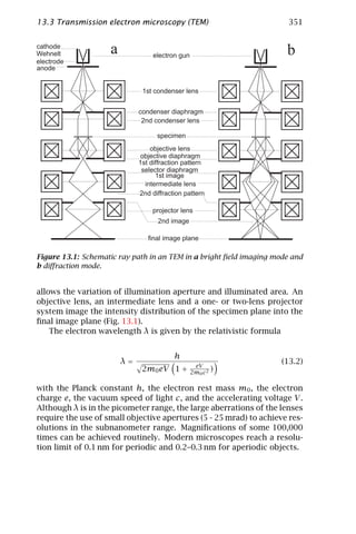

![13.3 Transmission electron microscopy (TEM) 353
plane. In summary, imaging in the ideal microscope reproduces the
object by a double Fourier transform times a linear magnification:
1
FF IP (ζ, η) = TOP (ζ, η) (13.4)
M
where FF IP and TOP denote the Fourier transforms of fF IP and tOP , M
the magnification, and ζ and η the spatial frequency components in x-
and y-direction.
On first sight, this looks like an ideal situation for imaging, providing
a simple projection of the phase and amplitude changing potentials
of the sample studied. Unfortunately, lens aberrations in a real TEM
as well as the necessity for defocus to visualize phase contrast lead
to contrast transfer modulations that change the sample information
recorded in one single image.
13.3.2 Real TEM
For real magnetic lenses, the paraxial approximation of the particle
optics model is no longer valid and higher-order terms in the equations
of motion for the electrons have to be considered. These terms account
for geometrical aberrations in a real microscope; chromatic aberrations
can be introduced via consideration of small changes in electron energy
and lens strength.
In the wave-optical approach, a thorough analysis of the situation
leads to the concept of the contrast transfer function (CTF) [6, 7], the
electron optical analogue to the optical transfer functions of light op-
tical devices (Chapter 20). Independent of specimen structure, the CTF
describes the imaging properties of the microscope.
The double Fourier transform times linear magnification as men-
tioned in Eq. (13.4) has to be multiplied by the CTF that contains the
effects of limited illumination and objective apertures, lens aberrations
and the energy spread of the electrons:
1
FF IP (ζ, η) = CT F (ζ, η)TOP (ζ, η) (13.5)
M
Thus, image formation in a TEM can be regarded as a filtering oper-
ation, the filter function CTF not being equal to unity in a real micro-
scope. Different spatial frequencies will be transferred with different
weights (Fig. 13.2).
In the following, the most important imperfections of real electron
optical systems and their contributions to phase shifting and resolution
limiting will be listed.](https://image.slidesharecdn.com/computervision-handbookofcomputervisionandapplicationsvolume1-sensorsandimaging-120205081125-phpapp02/85/Computer-vision-handbook-of-computer-vision-and-applications-volume-1-sensors-and-imaging-378-320.jpg)


![356 13 Electron Microscopic Image Acquisition
original object, it is absolutely necessary to correct for the CTF either
by combining information from defocus series (Section 13.8) or—most
recently—by improving the optical properties of the lens, for example,
by correction of the spherical aberration [8]. The latter correction leads
to an almost perfect transfer of the amplitude contrast. In the case
that samples provide strong amplitude contrast (as, e. g., for metals
or typical samples in solid state physics), this leads to almost perfect
images that are close to the ideal projection of specimen potentials,
and thus are being easily interpreted.
13.3.3 Imaging modes in the TEM
In principle, two modes of imaging can be distinguished for the con-
ventional, nonanalytical TEM: first, the imaging of the specimen itself to
visualize directly the spatial distribution of an object; and second, the
imaging of electron diffraction patterns of a given sample, thus record-
ing the amplitudes of Fourier structure factors of the spatial distribu-
tion only. These two modes are realized in the TEM by changing the
excitation current of the first projective lens that either magnifies the
first intermediate image formed by the objective lens or the first diffrac-
tion pattern in the back focal plane of the objective lens (Fig. 13.1).
On first sight, electron diffraction seems not to be very useful com-
pared to direct imaging, as all the phase information of the structure
factors is lost. However, it is relatively easy to obtain high-resolution
diffraction patterns of crystalline samples that give unique informa-
tion about the 3-D structure of the crystal, lattice excitations, or mul-
tiple elastic-inelastic scattering (Kikuchi bands in the case of dynamic
scattering on thick samples). Also for biological samples it is advanta-
geous to study crystalline arrays. Such specimens are extremely sus-
ceptible for beam damage, thus electron diffraction is the method of
choice to obtain high-resolution structure factor amplitudes because it
has a much better signal-to-noise ratio than comparable imaging (Sec-
tion 13.9).
For the normal imaging of an object TEM electron optics allows a
large variety of different techniques to obtain various aspects of the
specimen information contained in the transmitted electron beam.
Bright-field mode (BF). In conventional imaging in the BF mode, a
centered objective diaphragm (the corresponding objective apertures
are 5-20 mrad) that rejects electrons scattered into large angles leads to
scattering contrast. Therefore, the amount of transmitted and collected
electrons depends on the objective aperture, the electron energy and
the mean atomic number and mass thickness (the product of dens-
ity and thickness) of the specimen. In a thin specimen, it decreases](https://image.slidesharecdn.com/computervision-handbookofcomputervisionandapplicationsvolume1-sensorsandimaging-120205081125-phpapp02/85/Computer-vision-handbook-of-computer-vision-and-applications-volume-1-sensors-and-imaging-381-320.jpg)


![13.5 Analytical transmission electron microscopy 361
s o u rc e d e te c to r
illu m in a tio n d e te c to r
a p e r t u r e θi l l a p e r t u r e θd e t
s p e c im e n
o b je c tiv e p ro b e
a p e r t u r e θo b j a p e r t u r e θp r
o b je c tiv e
le n s
d e fle c tio n
c o ils
im a g e s o u rc e
T E M S T E M
Figure 13.3: Schematic ray path in a TEM and a STEM. Redrawn from [9].
linear photodiode or CCD arrays (parallel detection) or photomultipli-
ers over which the spectrum is shifted (serial detection) are employed.
The electron current distribution in the detector plane is a far-field
diffraction pattern of the illuminated object area. Therefore, recording
that pattern with an array of small detectors rather than one large de-
tector allows a wide range of structural and phase information to be
extracted from each object point by digital data processing.
Despite being superior to TEMs in most respects, dedicated STEMs
are today only very rarely used for some special applications due to
their complicated use and maintenance.
13.5 Analytical transmission electron microscopy
As a general trend, transmission electron microscopy moves more and
more away from simple imaging towards analytical methods, above all
element analysis. Electron energy loss spectroscopy (EELS) in the en-
ergy filtering transmission electron microscope (EFTEM) and electron-
probe microanalysis (EPMA) in the STEM provide a sensitive means of
obtaining image data specific to chemical elements or chemical phases
present in the sample, thereby introducing another ’element dimension’
to the two-dimensional image.](https://image.slidesharecdn.com/computervision-handbookofcomputervisionandapplicationsvolume1-sensorsandimaging-120205081125-phpapp02/85/Computer-vision-handbook-of-computer-vision-and-applications-volume-1-sensors-and-imaging-386-320.jpg)
![362 13 Electron Microscopic Image Acquisition
13.5.1 Electron probe x-ray microanalysis
During the past decades, electron-probe x-ray microanalysis (EPMA,
also called EDX (energy dispersive x-ray microanalysis) has become
a standard technique for the qualitative and quantitative analysis of
the element composition of very small samples. Here, the character-
istic and continuum x-ray quanta generated in the sample by the elec-
tron beam are counted by a semiconductor detector and the resulting
x-ray spectra processed quantitatively to obtain absolute concentra-
tions or concentration ratios of the elements present in the specimen
[10, 11]. When carried out in a scanning transmission electron micro-
scope (STEM), a high spatial resolution of a few nanometers and a sen-
sitivity of 10−15 g of an element can be reached, limited by the counting
statistics, the diameter of the electron probe and the thickness of the
object to be analyzed. Digitally storing the x-ray spectrum from every
pixel in a scanning image allows computation of compositional maps.
However, EDX imposes some severe disadvantages that limit its use-
fulness especially for biological specimens: in biological samples one
is generally interested in the detection of light elements with an atomic
number up to 20 such as O, Na, Mg, P, S, Cl, K and Ca. Since the x-ray
quantum yield decreases with falling atomic number in favor of non-
radiative processes and since only a small portion of the x-ray quanta
can be detected due to the limited size of the detector entrance window
(covering only about 10 % of the solid angle into which x-ray radiation
is emitted), there is a need for long acquisition times and high beam
intensities. This also results in high electron doses that produce radia-
tion damage of the delicate specimen, thus causing drift problems, loss
of the elements to be measured, and overall mass loss.
13.5.2 Energy-filtering electron microscopy
Facing these disadvantages, it seems natural to look for the primary
process of the electron beam-target interaction, that is, the elastic and
inelastic electron scattering that results in a respective energy loss of
the beam electrons, rather than to observe the ineffective secondary
process, that is, the generation of x-rays. By collecting and analyzing
the electrons transmitted through the sample spectroscopically up to
80 % of the inelastic collision events can be detected. This method—
known as electron energy loss spectroscopy (EELS)—results in smaller
electron doses needed to obtain the same amount of information as
with EDX methods. Therefore, shorter acquisition times, less beam
damage to the specimen or higher sensitivity especially for the light
elements can be achieved [12].
After the incident beam electrons with an initial kinetic energy E0
have passed the sample, they are separated according to their kinetic](https://image.slidesharecdn.com/computervision-handbookofcomputervisionandapplicationsvolume1-sensorsandimaging-120205081125-phpapp02/85/Computer-vision-handbook-of-computer-vision-and-applications-volume-1-sensors-and-imaging-387-320.jpg)
![13.5 Analytical transmission electron microscopy 363
zero-loss peak
intensity [arbitrary units]
plasmon peak
ionization edge
x 10 x 104
0 10 50 200
energy loss [eV]
Figure 13.4: Schematic electron energy loss spectrum.
energy E by means of an energy dispersive electron spectrometer to
produce what is called an electron energy loss spectrum, showing the
scattered intensity as a function of the energy loss ∆E = E0 − E of the
beam electrons.
A schematic energy loss spectrum is showed in Fig. 13.4. The first
zero-loss or elastic peak at 0 eV represents those electrons that are elas-
tically scattered into small angles.
The second plasmon-loss or low-loss peak in the region 5-50 eV rep-
resents the inelastic scattering from outer-shell electrons and shows
discrete energy losses in multiples of the plasmon energy of the re-
spective material. Towards higher energy losses, the plasmon peak
decreases smoothly according to a power of the energy loss.
Core-loss or ionization edges are superimposed on the plasmon loss
background at higher energy losses: a sharp rise in the scattered inten-
sity occurs on the ionization threshold of an inner-shell excitation—the
energy loss that approximately equals the binding energy of the corre-
sponding atomic shell—and decreases in a long tail. Since the binding
energies depend on the atomic number of the atom, the resulting edges
in the energy loss spectrum are characteristic for the elements present
in the specimen. Measuring the area under these edges allows for quan-
titative element analysis. The chemical binding type of the specimen
atoms results in a fine structure of the edges that can give information
on the chemical environment.
Similar to EDX, EELS can be carried out using a highly focused elec-
tron probe, for example, in the STEM, which allows the acquisition of
the electron energy loss spectrum from the illuminated area by a serial
detector such as a photomultiplier (serial EELS ) or a parallel detector
similar to a photodiode array, a CCD or TV camera (parallel EELS ). If
the electron probe is directed to scan over the specimen, the acquired
two-dimensional set of spectra can be processed to obtain an element
mapping of the scanned area (spectrum-imaging). Using an imaging
energy filter and parallel illumination, EELS offers the possibility of
recording images to which only electrons of a defined energy loss con-](https://image.slidesharecdn.com/computervision-handbookofcomputervisionandapplicationsvolume1-sensorsandimaging-120205081125-phpapp02/85/Computer-vision-handbook-of-computer-vision-and-applications-volume-1-sensors-and-imaging-388-320.jpg)
![364 13 Electron Microscopic Image Acquisition
tribute, so-called energy-selective or energy-filtered images. Taking 2,
3 or more energy-filtered images at different energy losses around ele-
ment specific features of the spectrum (electron spectroscopic imaging
(ESI) allows qualitative and semiquantitative element-specific imaging.
If whole series of energy-selective images at constant energy intervals
are recorded, spectra can be extracted from these series by means of
digital image processing (image EELS ). For that purpose, regions of in-
terest (ROI) are outlined in one of the images or in a separately recorded
high-contrast image. The pixel gray values from within a ROI have then
to be averaged and these average values arranged along the energy-loss
axis according to the energy intervals used during recording to end up
in a spectrum from that ROI.
With the advance in electron optics, electron detector and computer
technology during the last ten years, the routine use of EFTEM tech-
niques in EM image acquisition has become more and more feasible.
However, the large and often highly varying background underlying
the characteristic energy-loss signals demands considerable knowledge
and experience from the operator and takes far more effort for data
processing than in EDX microanalysis.
13.6 Scanning electron microscopy (SEM)
An image formation mechanism completely different from transmis-
sion microscopy is used in scanning electron microscopy (SEM). Mainly
the surface topology of thick objects is imaged. While probe form-
ing and scanning is carried out in the same way as in the STEM (Sec-
tion 13.4), there are no transmitted electrons that could be detected
from bulk specimens. The object information is contained in the var-
ious shares and emission directions of secondary and backscattered
electrons. Modern SEMs achieve a resolution in the range of up to 1
to 3 nm. SEM offers a high depth of field and delivers topographical,
magnetic, chemical and electronic state information of the sample.
13.6.1 Signal generation
The signal is generated at the specimen surface or within the speci-
men by scanning it with a fine electron probe. The signal consists of
backscattered electrons (BSE), secondary electrons (SE, Section 13.2) and
Auger electrons [13, 14]. Compared to SE, Auger electrons are emitted
from the specimen in such low numbers that, because of the low signal-
to-noise (S/N) ratio, they can be neglected in a conventional SEM; BSE
and SE are generated in sufficient numbers if high brightness electron
sources—LaB6 or field emitter—are used. Due to the low energy of SE](https://image.slidesharecdn.com/computervision-handbookofcomputervisionandapplicationsvolume1-sensorsandimaging-120205081125-phpapp02/85/Computer-vision-handbook-of-computer-vision-and-applications-volume-1-sensors-and-imaging-389-320.jpg)
![13.6 Scanning electron microscopy (SEM) 365
Conventional type SEM In-lens type SEM
Primary Primary
electrons electrons
lens pole piece
detector
specimen
specimen
SE
es
BS c
E e ape
sc
ap dep
ed th
ep
th
Figure 13.5: Signal detection in the SEM. Schematic detection of SE and BSE in a
conventional below-the-lens type of SEM (redrawn from Reimer and Pfefferkorn
[14]) compared to a high resolution “in-lens” type SEM.
compared to BSE, they can be separated by applying a small positive or
negative bias to the detector front end.
Another prerequisite for high-resolution SEM is a probe size of about
1 nm in order to deliver a highly localized signal. Analogous to the
minimum disk of confusion in the TEM, the minimum achievable spot
size is given by Eq. (13.13). A probe size of less than 1 nm as obtained
in STEM can be produced in an “in-lens” field emission SEM (FESEM)
[15]. The different arrangements of the specimen and the detectors in
an “in-lens” FESEM compared to a conventional (FE)SEM affect the signal
registration and contrast in the “in-lens” type FESEM (Fig. 13.5).
Electrons emitted from the sample with an energy below the arbi-
trary value of 50 eV are classically called secondary electrons (SE) with
a further classification into SE produced by the primary beam (SE I) and
SE produced by BSE (SE II). The volume from which SE I emerge is given
by their escape depth and the probe size. This volume being very small,
SE I carry the high spatial resolution information; SE II may be emitted
from an area of several microns squared (cross section of the SE escape
depth with the BSE escape volume), thus reducing the SE I signal con-
trast; SE generated by BSE at the lower part of the column (pole piece)
and at other parts of the specimen chamber (SE-III ), and SE generated
at the final aperture (SE-IV ) contribute disturbingly to the SE-I and SE-II
signal emitted from the sample. The SE-III, which account for 60-70 %
of the SE signal in a conventional type SEM [16] do not contribute to the](https://image.slidesharecdn.com/computervision-handbookofcomputervisionandapplicationsvolume1-sensorsandimaging-120205081125-phpapp02/85/Computer-vision-handbook-of-computer-vision-and-applications-volume-1-sensors-and-imaging-390-320.jpg)
![366 13 Electron Microscopic Image Acquisition
collected signal in an in-lens type SEM, because the SE detector is posi-
tioned behind the condenser/objective lens and the specimen between
the two pole pieces of the immersion lens [17]. In other words, the S/N
ratio and the contrast in an ‘in-lens’ type SEM depend therefore mainly
on the SE-I and SE-II signal and, besides the different geometrical ar-
rangements, may be quite different compared to the contrast obtained
in a conventional SEM.
Secondary electron imaging. The high resolving SE-I cannot be sepa-
rated from the SE-II. However, to obtain high-resolution images (< 3 nm)
with the SE-imaging mode, a way has to be found to enhance the signal
generated at the spot of incidence against the SE-II signal. Especially on
biological specimens, the SE-II signal is even enlarged due to a larger
electron interaction volume in low atomic number specimens.
The insufficient SE emission and its unsatisfactory S/N ratio from
specimens with low atomic numbers (e. g., biological samples) and in-
duced charging effects during irradiation made metal coating a power-
ful tool for SE imaging of biological samples at low and high magnifi-
cation [18, 19]. One way to increase the high resolution topographic
signal on biological samples is to coat the surface with a thin metal
film (1–2 nm). Such a thin metal film localizes the signal at the sur-
face of the specimen and reduces charging effects. A way to separate
the high resolution signal (SE-I) from the diffuse SE-II signal is to use a
coating film that has a low BSE coefficient, hence no or very few BSE are
produced. Only the SE-II produced by the BSE from the interaction vol-
ume in the biological sample below such a coating film will contribute
to the SE-image. Various light metals fulfill this condition, and thin
chromium films have proven to reveal a high SE-I signal and therefore
high resolution in SEM. Higher resolution can be achieved with the help
of fine-grained tungsten (W) films [20] due to a clear distinction and
hence localization of the fine metal grain (1–3 nm) against the vacuum
or biological material.
Backscattered electron imaging. BSE have energies of 50 eV to the
full primary beam energy with the major fraction around the primary
energy and emerge from an area of up to a few microns squared. They
therefore also contain information from beneath the surface. High-
resolution BSE (BSE-I), generated in the specimen with low energy loss
in the area of probe incidence differ from other BSE (BSE-II) that emerge
after multiple scattering and high energy loss at some distance from
the probe. With the BSE-I signal collected from highly tilted bulk-metal
or gold-coated specimens, high resolution (2 nm) in SEM with short fo-
cal lenses has been demonstrated in the low-loss imaging mode [21].
Walther and Hentschel [22] demonstrated that even from an untilted
bulk biological specimen shadowed with 2 nm platinum-carbon and sta-](https://image.slidesharecdn.com/computervision-handbookofcomputervisionandapplicationsvolume1-sensorsandimaging-120205081125-phpapp02/85/Computer-vision-handbook-of-computer-vision-and-applications-volume-1-sensors-and-imaging-391-320.jpg)
![13.6 Scanning electron microscopy (SEM) 367
a b c d
Figure 13.6: High-resolution SE-contrast from thin coating films. Types of sur-
face contrast produced by specimens coated with a thin film. a Nontopographic
contrast types are the atomic number contrast and b the mass-thickness con-
trast. c Topographic contrast types are the particle contrast d and the edge
brightness contrast.
bilized with 10 nm carbon, sufficient BSE are generated to form an im-
age with high resolution.
13.6.2 Contrast mechanisms
The basic contrast-forming mechanism in SEM is topographic contrast:
the larger the angle between incident beam and surface normal, the
larger the number of secondary electrons that lie within their escape
depth and thus contribute to the SE signal. The resulting SE image
resembles a photograph of the object taken from the direction of the
electron beam with the object illuminated from the direction of the
detector.
Contrast in the SEM of thin coated specimens (<2 nm) is obtained
because the SE and BSE signals vary with the film thickness of thin
coating films parallel to the incident beam. The different SE contrast
mechanisms in high-resolution SEM of thin coated specimens are shown
in Fig. 13.6. The so-called mass thickness contrast (Fig. 13.6b) allows
imaging structures of a few nanometers in size [19, 23]. Different mass
thicknesses can also be seen by the electron probe on a coated slope,
revealing signal variations according to the steepness of the slope. An-
other contrast mechanism is the different SE- and BSE-yield with vary-
ing atomic number Z (material or atomic number contrast, Fig. 13.6a),
which is stronger for BSE than for SE [24]. Special contrast effects ap-
pear if the electron probe is close or within the SE-escape depth at a
border (Fig. 13.6d). The contrast of such a border is enhanced due
to the emission of a higher portion of SE that still can leave the close
surface. This signal can exceed the maximum signal of a film with a
thickness corresponding to the SE-escape depth. The same effect also
enhances the contrast of small particles (particle contrast, Fig. 13.6c),
if their diameter is smaller than twice the SE-escape depth.](https://image.slidesharecdn.com/computervision-handbookofcomputervisionandapplicationsvolume1-sensorsandimaging-120205081125-phpapp02/85/Computer-vision-handbook-of-computer-vision-and-applications-volume-1-sensors-and-imaging-392-320.jpg)
![368 13 Electron Microscopic Image Acquisition
The magnetic state of the specimen surface as well as electric sur-
face potentials alter SE- and BSE-yield and allow magnetic contrast and
voltage contrast imaging. Energy-dispersive x-ray (EDX) detectors are
routinely used in the SEM to detect the x-rays that are generated by the
incident electrons inside the specimen. Counting the characteristic x-
ray quanta allows mapping and quantification of the chemical elements
present in the specimen.
Recent improvements in electron optics made it possible to work
with low acceleration voltages of 200 eV to 5 kV (LVSEM, low-voltage
scanning electron microscopy) without decreasing resolution, thus al-
lowing control of the penetration depth of the incident electrons and
therefore varying the depth of the imaged surface layer even for un-
coated specimens. Another development, the environmental scanning
electron microscope (ESEM), allows microscopy of fully hydrated bio-
logical specimens under normal conditions, imaging of water layers,
dynamic events and chemical reactions. Reconstruction of the 3-D ob-
ject topography is possible by taking images under different directions
of illumination and digitally recovering the 3-D information.
13.7 Preparation techniques
Specimen preparation is the most crucial step in electron microscopic
image acquisition. Poor preparation will lead to restricted image infor-
mation or even to the constitution of artifacts. As, with a few excep-
tions, electron microscopes have to be operated at high vacuum, it is
not possible to use living biological specimens as in a light microscope.
Living specimens have to be adequately processed by fixation, dehydra-
tion and coating or embedding in plastic resins, which also raises their
ability to withstand beam-induced structural damage [25]. The need
for very thin, electron-transparent specimens requires these embed-
ded preparations to be cut into ultrathin sections by ultramicrotomy
using glass or diamond knives. These sections have thicknesses of typ-
ically 50 to 150 nm. In HVEM, sections a few hundred nanometers thick
can be studied. Hard inorganic solids such as ceramics or metals may
be crushed or first cut into slices with diamond saws and then thinned
by mechanical polishing, electropolishing or ion milling. Ultramicro-
tome sections and small crunching chips must be supported by small
metal grids, if necessary with a supporting carbon or polymer film, to
be introduced into the microscope column.
Staining with heavy metals (“negative staining”) allows fine struc-
tures, supramolecular assemblies and single macromolecules to be vi-
sualized at a high resolution. Specific macromolecules can be high-
lighted by various labeling techniques. High-resolution imaging of spec-
imen surfaces in the TEM can be achieved by the use of replica tech-](https://image.slidesharecdn.com/computervision-handbookofcomputervisionandapplicationsvolume1-sensorsandimaging-120205081125-phpapp02/85/Computer-vision-handbook-of-computer-vision-and-applications-volume-1-sensors-and-imaging-393-320.jpg)
![13.8 Digital image processing of electron micrographs 369
niques, where thin metal films are evaporated onto the sample to be
examined in the microscope after removing the original specimen.
Conventional chemical fixation techniques for EM specimens very
often lead to preparation artifacts that can be avoided using cryofix-
ation techniques that are of increasing importance especially in bio-
logical applications. Here, rapid freezing of the specimen is used to
achieve an optimum conservation of the native ultrastructure. Freeze-
fracture and freeze-etching, two other freeze-preparation techniques,
use cleaving of the frozen specimen to reveal the interior of cells and
cell membranes.
13.8 Digital image processing of electron micrographs
The electron micrograph can be made available as a matrix of pixel gray
values either from direct digital image acquisition with a CCD camera or
adequate transformation from a photographic film or TV image in the
TEM, or by direct digital acquisition in a scanning microscope [25, 26].
It is obvious that all conventional image processing techniques can then
be applied to such image data. The whole palette of digital image en-
hancement tools can be used for visual improvement of the images
acquired: adjusting brightness and contrast, gamma correction, sharp-
ening, deblurring, or removing background structures (Chapters 5 and
6). It becomes especially necessary to use these methods to preprocess
very low signal-to-noise ratio images for image alignment and extensive
image averaging.
Electron micrographs recorded with very low electron doses, for ex-
ample, tend to be very noisy. If the image contains a sufficient number
of identical structures such as cellular organelles or macromolecules, it
is possible to average over those to obtain a noise-reduced image (Chap-
ter 7). This averaging of low-dose images requires motif-detection pro-
cedures to select similar structures (Chapter 10) and cross-correlation
algorithms to position, orient and align them. Image alignment can be
achieved by computing the necessary shift vectors (Chapter 9) from the
2-D cross-correlation between two subsequent images. Proper align-
ment is particularly essential to the processing of electron micrograph
series. For the evaluation of periodic structures in the object, fast
Fourier transform (FFT) (Chapter 3) can be used, because 2-D FFT of the
image provides the diffraction pattern of the imaged specimen area. It
can also be used to control aberrations, defocus, astigmatism and other
lens defects. The image may also be filtered in Fourier space and then
inversely transformed to perform digital filtering without loss of phase
information.
As in light optical microscopy it is also necessary to correct the
image information for the point spread function of the microscope.](https://image.slidesharecdn.com/computervision-handbookofcomputervisionandapplicationsvolume1-sensorsandimaging-120205081125-phpapp02/85/Computer-vision-handbook-of-computer-vision-and-applications-volume-1-sensors-and-imaging-394-320.jpg)

![13.9 Imaging examples 371
Figure 13.7: Image of an epitaxial Si(111)/CoSi interface illustrating the con-
trast delocalization as image artifact due to spherical aberration. Images a
and b are taken without Cs correction at different defocus values: a Scherzer
focus; b Lichte focus, Cs = 1.2 mm). Image c shows the identical sample area in
the corrected TEM at Scherzer defocus with a remaining Cs = 0.05 mm. Figure
from Haider et al. [8] courtesy Nature (London), Macmillan Magazines Ltd.
cal samples embedded in glucose or vitrified ice or imaging near atomic
resolution on thin inorganic samples. In a few cases with dedicated
instrumentation it was possible to resolve biological molecules to the
molecular level (e. g., Bacteriorhodopsin [27], Light Harvesting Complex
LHC II [28], and Tubulin [29]).
As a complement to direct imaging, the diffraction of electrons at
crystalline samples is also widely used.
13.9.1 Imaging at atomic resolution
Imaging of atom columns in crystalline samples is one application of EM
necessary to find solutions to problems in modern solid state physics or
material sciences. To overcome the optical flaws of conventional instru-
mentation, different methods have been alternatively studied. These
include electron holography, high-energy TEM, and the correction of
lens aberrations in the TEM. Whereas the first two methods try to work
around the intrinsic optical problems of conventional TEMs, the work
on a corrected TEM tries to reduce the spherical aberration of the ob-
jective lens to get a more ideal, directly interpretable image.
Figure 13.7 shows the differences between imaging using a conven-
tional objective lens and a lens system with vanishing Cs (Cs corrector).
As expected from theory and light optical devices, finite spherical aber-
ration leads to an increased error disk of each image point and thus
to contrast delocalization, contrast decrease, and lower resulting res-
olution and structural interpretability. The recent development of the
electron optical corrector elements must therefore be seen as a major
milestone in electron optical imaging.](https://image.slidesharecdn.com/computervision-handbookofcomputervisionandapplicationsvolume1-sensorsandimaging-120205081125-phpapp02/85/Computer-vision-handbook-of-computer-vision-and-applications-volume-1-sensors-and-imaging-396-320.jpg)
![372 13 Electron Microscopic Image Acquisition
Figure 13.8: Light Harvesting Complex II, electron micrograph (left, from
Kühlbrandt [30], courtesy Nature (London), Macmillan Magazines Ltd.) and
electron diffraction pattern (right, from Wang and Kühlbrandt [31], by copy-
right permission of Academic Press, San Diego).
13.9.2 Imaging of biological samples
In contrast to inorganic material, biological samples cannot be imaged
directly without great preparative efforts and dedicated instrumenta-
tion. The reason for this is the atomic composition of biological sam-
ples that almost completely consist of light atoms such as H, C, O, N,
and minor contributions of P, S and others. As was discussed in Sec-
tion 13.7, conventional preparation techniques have been developed
that use heavy atom staining of the biological sample and the imaging of
this stain instead of the biological sample itself. Obtainable maximum
structural resolutions for such samples vary with specimen thickness
and preparation technique between about 2 and 10 nm. Even if this res-
olution seems to be very limited, applying these methods to biological
material many interesting questions have been answered and will be
answered in the future.
To achieve higher structural resolution as is needed, for instance,
for the determination of molecular structures in structural biology new
preparation methods were necessary. With the development of cryo-
techniques it is possible to study cooled samples in dedicated cryo-
microscopes. In such instruments samples are cooled down to liquid
nitrogen (-196 °C) or liquid helium temperature (-269 °C). At this temper-
ature samples are less susceptible to beam damage and even the light
atoms of biological material can then be imaged. However, compared to
material sciences samples, a much lower electron dose has to be used
for imaging, which results in very noisy images. Therefore the obtain-
able resolution from such images is largely dependent on good imaging
strategies to average over large ensembles of individual particles.](https://image.slidesharecdn.com/computervision-handbookofcomputervisionandapplicationsvolume1-sensorsandimaging-120205081125-phpapp02/85/Computer-vision-handbook-of-computer-vision-and-applications-volume-1-sensors-and-imaging-397-320.jpg)
![13.9 Imaging examples 373
Figure 13.9: Light Harvesting Complex II, 3-D representation. From Kühlbrandt
et al. [28], courtesy Nature (London), Macmillan Magazines Ltd.
Such averaging is performed best on crystalline samples. All the
molecular structures obtained by EM resulted from studies of 2-D pro-
tein crystals, that is, crystalline monolayers of proteins. Such crystals
can either be conventionally imaged or electron diffraction patterns can
be recorded from them. Electron diffraction patterns of well-ordered
protein crystals diffract very often to a resolution better than 2 Å. Un-
fortunately, imaging of such crystals does not in general yield phase
information to the same resolution. Images are affected by specimen
drift, specimen charging and the low signal-to-noise ratio of the images.
Up to now, typical resolution limits for imaging on dedicated TEMs are
of the order of 3-4 Å. Combining data from higher angle specimen tilt
series, it is then possible to calculate 3-D density maps at this resolu-
tion. This resolution is sufficient for the determination of the molecu-
lar structure, that is, the known amino acid sequence can be built into
such densities as a molecular amino acid chain. For a fine example that
shows the application of all these techniques see the work on bacteri-
orhodopsin crystals [27]. Work on the Light Harvesting Complex II is
shown in Figs. 13.8 and 13.9, which illustrate typical rotary shadowing
images of crystals, electron diffraction patterns from such crystals, and
the finally obtained 3-D density maps together with the built-in amino
acid chain.
Besides the successful studies on 2-D crystalline assemblies of bi-
ological material other methods for analyzing objects with lower sym-
metry have been developed. Such systems are helical objects (actin
filaments), icosahedral objects (viruses), or—without any symmetry—](https://image.slidesharecdn.com/computervision-handbookofcomputervisionandapplicationsvolume1-sensorsandimaging-120205081125-phpapp02/85/Computer-vision-handbook-of-computer-vision-and-applications-volume-1-sensors-and-imaging-398-320.jpg)
![374 13 Electron Microscopic Image Acquisition
Figure 13.10: Cryomicrographs showing top-view images of the calcium re-
lease channel as a tilted and b untilted specimen. Corresponding molecules are
labeled with numbers. From Radermacher et al. [32], by copyright permission
of Rockefeller University Press.
assemblies of a nonsymmetric particle. Such “single particles” are spe-
cial in the sense that no averaging methods can be applied unless a thor-
ough classification and alignment procedure was applied to the image
data set. Appropriate methods have been developed by Frank and van
Heel; for a rigorous discussion of these methods see [33]. Because data
averaging and alignment is much more tedious for single particles than
for periodic objects, the structural resolution achieved up to now is not
as high as for 2-D crystals. The best examples are reconstructions of
viruses at 9 Å resolution (still applying icosahedral symmetry) [34] or
20-25 Å for ribosomes as large, asymmetric assemblies of protein and
RNA [35, 36].
A general problem for all 3-D reconstruction in electron microscopy
is the collection of the third dimension structural information from 2-
D projection images. This problem has in general been solved using
tomographic methods. For oriented samples such as 2-D crystals or
other specimens that have a preferential orientation, this is realized by
single axis tilting of the specimen in the microscope. Because the tilt
axes for individual objects are randomly oriented, merging data from
single axis tilted images give complete coverage in all three dimensions
(random conical tilt for single particles, tilt series of 2-D crystals). Fig-
ures 13.10 and 13.11 illustrate this situation for a membrane channel
protein. This flat biological object orients in only two views in the mi-
croscopical preparation (Fig. 13.11a,b, side view c does not occur in
micrographs). For technical details of the random conical tilt method
used here see [39]. In the case of completely random orientation of](https://image.slidesharecdn.com/computervision-handbookofcomputervisionandapplicationsvolume1-sensorsandimaging-120205081125-phpapp02/85/Computer-vision-handbook-of-computer-vision-and-applications-volume-1-sensors-and-imaging-399-320.jpg)
![13.9 Imaging examples 375
Figure 13.11: Stereorepresentation of the reconstruction of the calcium release
channel (Fig. 13.10) a cytoplasmic side b sarcoplasmatic side of the channel, c
side view. From Radermacher et al. [32], by copyright permission of Rockefeller
University Press.
the object in the micrograph, for example, Fig. 13.12 for E. coli ribo-
somes, images of untilted objects can be aligned and merged to obtain
the 3-D structure [35] (see van Heel [40] for technical details on direct
alignment of objects of unknown Eulerian angles).
13.9.3 Electron diffraction in material sciences
As has been pointed out for biological samples, electron diffraction
on crystalline samples is a powerful method to obtain additional high-
resolution information about the specimen. In contrast to the normal
parallel beam electron diffraction, convergent beams are often used in
material science. In contrast to the diffraction on biological samples
(Fig. 13.8), the corresponding diffraction patterns are not simple Bragg
spot patterns. Different techniques have been developed, and from
convergent beam patterns today many different kinds of information
on the 3-D structure can be collected. Typical examples of convergent
beam diffraction patterns are shown in Fig. 13.13 and Fig. 13.14.](https://image.slidesharecdn.com/computervision-handbookofcomputervisionandapplicationsvolume1-sensorsandimaging-120205081125-phpapp02/85/Computer-vision-handbook-of-computer-vision-and-applications-volume-1-sensors-and-imaging-400-320.jpg)
![376 13 Electron Microscopic Image Acquisition
a
b
Figure 13.12: a 70S ribosomes from Escherichia coli, visualized by cryo-electron
microscopy. Electron optical magnification 50,000×. b The ribosome at 15 Å,
reconstructed from 30,000 projections obtained by cryoelectron microscopy,
shown with a tRNA in the P-site position as experimentally found [37]. The
anticodon of the tRNA is in the vicinity of the channel that is thought to conduct
the messenger RNA [35], while the acceptor end (marked CCA) is seen to point
toward the opening of the tunnel that is believed to export the polypeptide chain
[38] [Prepared by Amy Heagle and Joachim Frank, Laboratory of Computational
Biology and Molecular Imaging, Wadsworth Center]; (see also Plate 8).
13.9.4 Element mapping in biology and material science
Often a quick and convenient way of producing chemical element maps
is ESI in the EFTEM (Section 13.5.2). Here one or more energy-filtered
images are acquired just before the onset of the interesting ionization
edge (pre-edge images) and another one just after the onset (post-edge
image).](https://image.slidesharecdn.com/computervision-handbookofcomputervisionandapplicationsvolume1-sensorsandimaging-120205081125-phpapp02/85/Computer-vision-handbook-of-computer-vision-and-applications-volume-1-sensors-and-imaging-401-320.jpg)
![13.9 Imaging examples 377
Figure 13.13: Convergent beam electron diffraction pattern from a MgAl2 O4
spinel single crystal obtained along the <100> zone axis. From such patterns
information can be obtained on crystal structure and space group, structure
factors and temperature factors (Debye-Waller-factors), charge density distri-
bution and bonding charge densities [Prepared by Joachim Mayer, MPI für Met-
allforschung, Stuttgart, Germany].
Figure 13.14: Large-angle convergent beam electron diffraction pattern ob-
tained with the Tanaka-technique on a LEO EM 912 microscope with zero loss
energy filtering. The pattern was obtained from an Al single crystal in <111>
orientation [Prepared by Joachim Mayer, MPI für Metallforschung, Stuttgart,
Germany].](https://image.slidesharecdn.com/computervision-handbookofcomputervisionandapplicationsvolume1-sensorsandimaging-120205081125-phpapp02/85/Computer-vision-handbook-of-computer-vision-and-applications-volume-1-sensors-and-imaging-402-320.jpg)

![13.9 Imaging examples 379
Figure 13.16: Bright field image and elemental distribution images for C, N,
O from a Si3 N4 -SiC composite ceramic prepared form polysilazan polymer pre-
cursors. The distribution of the Si3 N4 -, SiC-grains and the amorphous oxide can
be seen in the individual elemental distribution images. Elemental distribution
images obtained with the three window technique on the LEO EM 912 micro-
scope. Figure from Mayer [41], by copyright permission of Elsevier Science Ltd.,
Oxford, England.
olate the pre-edge background to the post-edge region according to
a function of the energy loss, the parameters of which are calculated
from the pre-edge image intensities for every pixel. The net element
distribution is then acquired by subtracting the calculated background
intensity from the post-edge image. Our example shows a conventional
bright-field image of a sintered polymer derived Si3 N4 /SiC-composite
ceramic (top left), a carbon map (top right), a nitrogen map (bottom
left) and an oxygen map (bottom right) obtained from the same sample
area by this three-window method.
13.9.5 SEM image examples
The advantage of SEM is that large bulk samples can be imaged with-
out or only slight fragmentation of the specimen and hence disturbing
its natural context. In addition, the large depth of focus in SEM al-
lows to image large and complex surface structures in focus and hence
makes SEM a powerful tool for the determination of surface structures.](https://image.slidesharecdn.com/computervision-handbookofcomputervisionandapplicationsvolume1-sensorsandimaging-120205081125-phpapp02/85/Computer-vision-handbook-of-computer-vision-and-applications-volume-1-sensors-and-imaging-404-320.jpg)


![13.10 References 383
many, Dr. M. Haider, CEOS GmbH, Heidelberg, Germany, Dr. W. Kühl-
brandt, MPI für Biophysik, Frankfurt, Germany.
13.10 References
[1] Glaser, W., (1952). Grundlagen der Elektronenoptik. Wien: Springer.
[2] Knoll, M. and Ruska, E., (1932). A contribution to geometrical electron
optics. Ann. Phys., 12:607–640.
[3] von Ardenne, M., (1938). Das Elektronen-Rastermikroskop. Theoretische
Grundlagen. Z. Phys., 109:533–572.
[4] Oatley, C. W., Nixon, W. L., and Pease, R. F. W., (1965). Scanning electron
microscopy. Adv. Electronics Electron Phys., 21:181–247.
[5] Hawkes, P. (ed.), (1985). The Beginnings of Electron Microscopy. Advances
in Electronics and Electron Physics, Suppl. 16. Orlando, FL: Academic Press.
[6] Thon, F., (1966). Defocus dependence of the phase contrast in the electron
microscopic image. Z. Naturforschung, 21a:476–478.
[7] Thon, F., (1971). Phase contrast electron microscopy. In Electron Mi-
croscopy in Material Science, U. Valdr, ed. New York: Academic Press.
[8] Haider, M., Uhlemann, S., Schwan, E., Rose, H., Kabius, B., and Urban, K.,
(1998). Development of the first spherical aberration corrected 200 kV
transmission electron microscope. Nature, 392:768–769.
[9] Reimer, L. (ed.), (1997). Transmission Electron Microscopy, 4th edition.
Berlin, Heidelberg, New York: Springer Verlag.
[10] Heinrich, K. and Newbury, D. (eds.), (1991). Electron Probe Quantization.
New York: Plenum Press.
[11] Scott, V., (1995). Quantitative Electron Probe Microanalysis. New York:
Ellis Horwood.
[12] Egerton, R. F., (1996). Electron Energy-loss Spectroscopy in the Electron
Microscope, 2nd edition. New York: Plenum Press.
[13] Joy, D. C., (1984). Beam interactions, contrast and resolution in the SEM.
Jour. Microsc., 136:241–258.
[14] Reimer, L. and Pfefferkorn, G., (1977). Rasterelektronenmikroskopie.
Berlin, Heidelberg, New York: Springer Verlag.
[15] Nagatani, T., Saito, S., and et al., (1987). Development of an ultra high
resolution scanning electron microscope by means of a field emission
source and in-lens system. Scanning Microscopy, 1(3):901–909.
[16] Peters, K. R., (1984). Generation, collection and properties of an SE-I en-
riched signal suitable for high resolution SEM on bulk specimen. In Elec-
tron Beam Interactions with Solids, D. F. Kyser, D. E. Newbury, H. Niedrig,
and R. Shimizu, eds., pp. 363–372. AMF O’Hare.
[17] Koike, H., Ueno, K., and Suzuki, M., (1970). Scanning device combined with
conventional electron micoscope. In Proc. 29th Ann. Meeting of EMSA,
p. 28.
[18] Echlin, P., (1979). Thin films for high resolution conventional scanning
electron microscopy. Scanning Electron Microsc., 2:21–30.](https://image.slidesharecdn.com/computervision-handbookofcomputervisionandapplicationsvolume1-sensorsandimaging-120205081125-phpapp02/85/Computer-vision-handbook-of-computer-vision-and-applications-volume-1-sensors-and-imaging-408-320.jpg)
![384 13 Electron Microscopic Image Acquisition
[19] Hermann, R. and Müller, M., (1991). High resolution biological scanning
electron microscopy: A comparative study of low temperature metal coat-
ing Techniques. Jour. El. Mic. Techn., 18:440–449.
[20] Wepf, R., Bremer, A., Amrein, M., Aebi, U., and Gross, M., (1992). Surface
imaging of F-actin filaments: a comparative study by SEM, TEM and STM,
Vol. III. Secretariado del Publicaciones de la Universidad de Granada.
[21] Wells, O. C., (1974). Resolution of the topographic image in the SEM.
Scanning Electron Microsc., I:1–8.
[22] Walther, P. and Hentschel, J., (1989). Improved representation of cell sur-
face structures by freeze substitution and backscattered electron imag-
ing. Scanning Microsc., 3:201–211.
[23] Wepf, R., Amrein, M., et al., (1991). Platinum/iridium/carbon: a high-
resolution shadowing material for TEM, STM and SEM of biological macro-
molecular structures. J. Microsc., 163(1):51–64.
[24] Reimer, L., (1979). Electron-specimen interaction. Scanning Electron Mi-
crosc., II:111–124.
[25] Glauert, A. (ed.), (1981). Practical Methods in Electron Microscopy. Am-
sterdam: North-Holland.
[26] Hawkes, P. (ed.), (1980). Computer Processing of Electron Microscopic Im-
ages. Berlin, Heidelberg, New York: Springer Verlag.
[27] Henderson, R., Baldwin, J., Ceska, T., Zemlin, F., Beckmann, E., and Down-
ing, K., (1990). Model for the structure of bacteriorhodopsin based on
high-resolution electron cryo-microscopy. Jour. Mol. Biol., 213:899–929.
[28] Kühlbrandt, W., Wang, D., and Fujiyoshi, Y., (1994). Atomic model of the
plant light-harvesting complex by electron crystallography. Nature, 367:
614–621.
[29] Nogales, E., Wolf, S., and Downing, K., (1998). Structure of the ab tubulin
dimer by electron crystallography. Nature, 391:199–203.
[30] Kühlbrandt, W., (1984). Three-dimensional structure of the light-
harvesting chlorophyll a/b-protein complex. Nature, 307:478–480.
[31] Wang, D. N. and Kühlbrandt, (1991). High-resolution electron crystallog-
raphy of light-harvesting chlorophyll a/b-protein complex in three differ-
ent media. Jour. Mol. Biol., 217(4):691–699.
[32] Radermacher, M., Rao, V., Grassucci, R., Frank, J., Timerman, A.,
Fleischer, S., and Wagenknecht, T., (1994). Cryo-electron microscopy
and three-dimensional reconstruction of the calcium release chan-
nel/ryanodine receptor from skeletal muscle. Jour. Cell Biol., 127:411–
423.
[33] Frank, J., (1996). Three-Dimensional Electron Microscopy of Macromolec-
ular Assemblies. San Diego: Academic Press.
[34] Böttcher, B., Wynne, S., and Crowther, R., (1997). Determination of the
fold of the core protein of hepatitis B virus by electron cryomicroscopy.
Nature, 386:88–91.
[35] Frank, J., Zhu, J., Penczek, P., Li, Y., Srivastava, S., Verschoor, A., Gras-
succi, R., Lata, R., and Agrawal, R., (1995). A model of protein synthesis](https://image.slidesharecdn.com/computervision-handbookofcomputervisionandapplicationsvolume1-sensorsandimaging-120205081125-phpapp02/85/Computer-vision-handbook-of-computer-vision-and-applications-volume-1-sensors-and-imaging-409-320.jpg)
![13.10 References 385
based on cryo-electron microscopy of the E. coli ribosome. Nature, 376:
441–444.
[36] Stark, H., Mueller, F., Orlova, E., Schatz, M., Dube, P., Erdemir, T., Zem-
lin, F., Brimacombe, R., and van Heel., M., (1995). The 70S Escherichia
coli ribosome at 23 Å resolution: fitting the ribosomal RNA. Structure, 3:
815–821.
[37] Malhotra, A., Penczek, P., Agrawal, R. K., Gabashvili, I. S., Grassucci, R. A.,
Juenemann, R., Burkhardt, N., Nierhaus, K. H., and Frank, J., (1998).
Escherichia coli 70S ribosome at 15 A resolution by cryo-electron mi-
croscopy: localization of fMet-tRNA(f/Met) and fitting of L1 protein. Jour.
Mol. Biol., in press.
[38] Beckmann, R., Bubeck, D., Grassucci, R. A., Penczek, P., Verschoor, A.,
Blobel, G., and Frank, J., (1997). Alignment of conduits for the nascent
polypeptide chain in the ribosome-Sec61 complex. Science, 278:2123–
2126.
[39] Radermacher, M., (1988). Three-dimensional reconstruction of single par-
ticles from random and nonrandom tilt series. Jour. Electr. Microsc. Tech.,
9:359–394.
[40] van Heel, M., (1987). Angular reconstitution: a posteriori assignment of
projection directions for 3D reconstruction. Ultramicroscopy, 21:111–
124.
[41] Mayer, J., (1996). Polymer-derived Si-based bulk ceramics: 2. Microstruc-
tural characterization by electron spectroscopic imaging. Jour. of the
European Ceramic Society, 15:717–727.](https://image.slidesharecdn.com/computervision-handbookofcomputervisionandapplicationsvolume1-sensorsandimaging-120205081125-phpapp02/85/Computer-vision-handbook-of-computer-vision-and-applications-volume-1-sensors-and-imaging-410-320.jpg)


![388 14 Processing of Ultrasound Images in Medical Diagnosis
Most clinical ultrasound imaging systems operate on the impulse-
echo principle Cho et al. [1], Hill [2]. A pulse train of acoustic waves con-
sisting of an rf sinusoidal carrier modulated by impulses of appropriate
form is launched into the region under investigation by means of one
or more piezocrystals. The reflected and backscattered acoustic waves
are collected by the same crystals in the intervals interspersed between
the transmitted impulses and converted into voltage signals. By pro-
cessing the received signal, an image of the variations of the acoustic
impedance of the area under investigation is formed. Figure 14.6 shows
typical B-mode images. Multiple reflections and diffraction are accom-
panying phenomena that affect the received signal and deteriorate the
ultrasound imaging. Furthermore, the acoustic signal is attenuated by
the tissue—with increasing frequency, the attenuation increases. Thus,
the depth up to which ultrasound imaging is feasible is limited by the
frequency. As, on the other hand, resolution increases with frequency,
trade-off between depth and resolution of imaging is inevitable.
To counteract the effects of attenuation, multiple reflection, refrac-
tion etc., techniques are developed with degrees of sophistication, which
ever increasingly go hand-in-hand with the availability of powerful dig-
ital electronics. These techniques employ the following measures:
1. Several (up to a few hundred) piezocrystals are employed in the
transmitting and receiving transducers.
2. Electronic beam forming and focusing techniques are employed.
3. Attenuation is compensated.
4. Several images are acquired, stored, and processed to obtain a re-
sulting image with a higher signal to noise ratio (SNR).
The image quality achievable is limited by the physics of ultrasound
and its interaction with tissue. One limiting factor of the fidelity of
imaging is the amplitude and phase aberration of the ultrasound waves.
A current topic of research and development is the compensation of
the effects of these aberrations. Generally, a huge volume of data is
generated and has to be handled. The processing of the beam-formed
signal is incoherent, that is, the voltage signal corresponding to the
superposition of received sinusoidal acoustic echo signals is envelope-
detected with no consideration being given to the phase. This leads to
interference of the echoes and gives rise to the familiar but disturbing
speckles in the image.
Ultrasound imaging was first employed in clinical diagnosis in the
“A-mode” in 1945. Here, the acoustic echoes (which depict the acoustic
impedance variations) in an organ or tissue along a scanning straight-
line direction were imaged. The technique became popular with the
advent of “B-mode” 2-D imaging systems, which were introduced sub-
sequently in the 1950s. These are the systems currently in widespread](https://image.slidesharecdn.com/computervision-handbookofcomputervisionandapplicationsvolume1-sensorsandimaging-120205081125-phpapp02/85/Computer-vision-handbook-of-computer-vision-and-applications-volume-1-sensors-and-imaging-413-320.jpg)


![14.2 Ultrasound imaging systems 391
B-mode
Figure 14.1: B-mode imaging of the heart.
tions of the amplitude are depicted as a function of the corresponding
depths at which these occur. This is the “A-mode” image. An alterna-
tive method of display is to make the brightness of a point moving in a
straight line corresponding to the propagation direction proportional
to the amplitude of the received signal. By successively sweeping the di-
rection of propagation in a plane and recording the series of “A-mode”
images as straight lines with varying brightness next to one another,
one obtains the “B-mode” image. Figure 14.1 shows the formation of a
B-mode image of the heart
To be able to interpret the image and study the relation between the
images and the acoustic properties of the organs and tissues that are
imaged, it is necessary to understand the mechanism of wave propaga-
tion. An exact analysis of the mechanism is the subject of continuing
research and is complex. In the following, basic equations according to
Cho et al. [1] are given.
14.2.1 Mechanisms of ultrasound wave propagation
The acoustic wave launched by the transducer is propagated in the
tissue as a longitudinal pressure wave that causes local variations of
pressure density and velocity of the medium. The tissue is assumed to
act like an isotropic nonabsorbing homogeneous fluid in which shear
forces are negligible. These and further assumptions make the prob-
lem mathematically tractable; however, they are valid only as approxi-
mations. The plane wave equation of acoustic waves in a homogeneous](https://image.slidesharecdn.com/computervision-handbookofcomputervisionandapplicationsvolume1-sensorsandimaging-120205081125-phpapp02/85/Computer-vision-handbook-of-computer-vision-and-applications-volume-1-sensors-and-imaging-416-320.jpg)


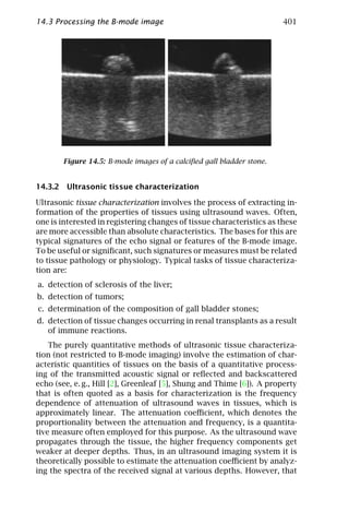


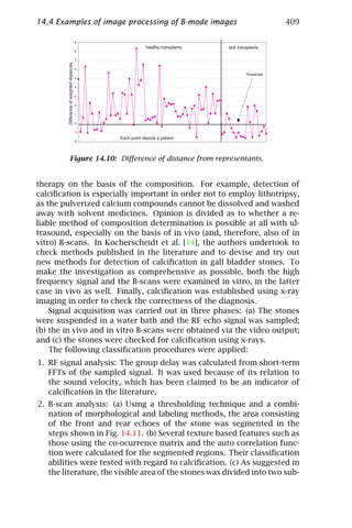


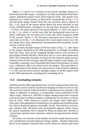


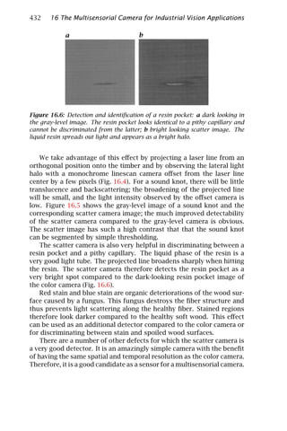


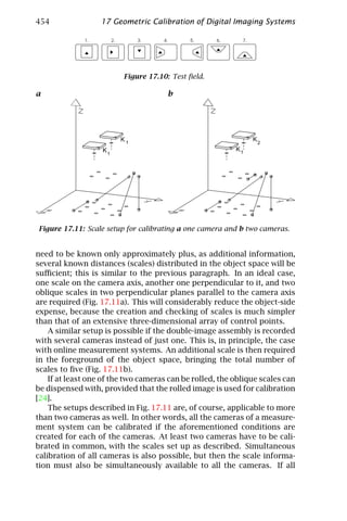


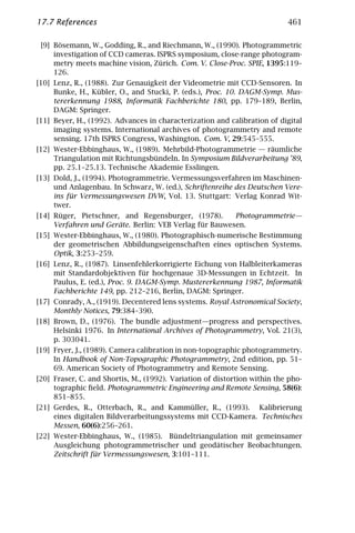


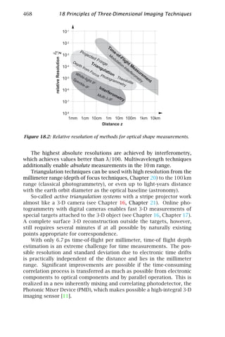


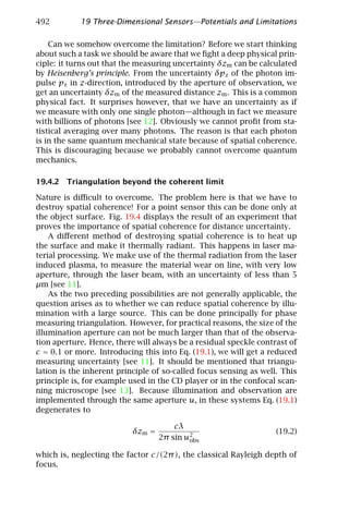


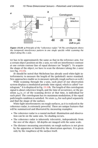


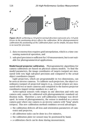


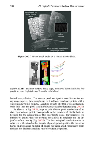
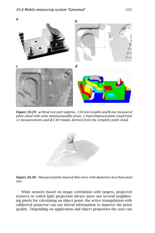
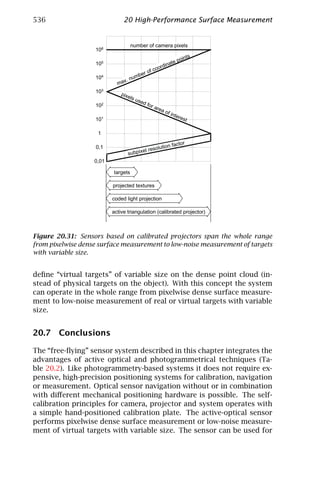


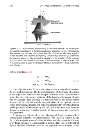


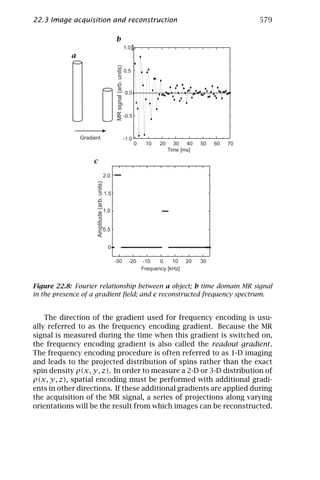


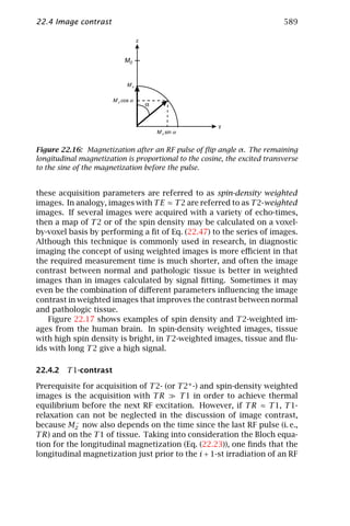


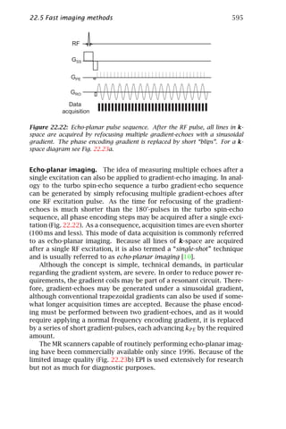

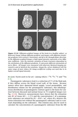


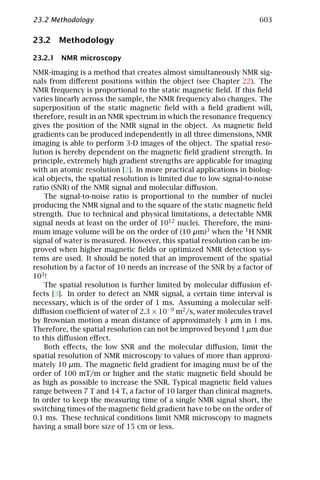
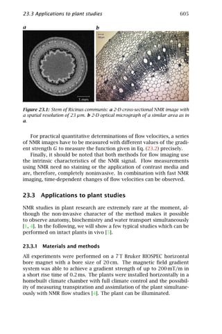

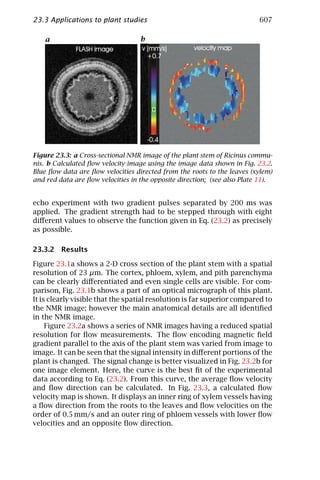
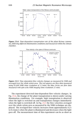
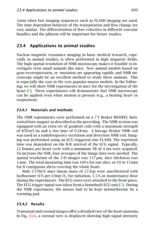

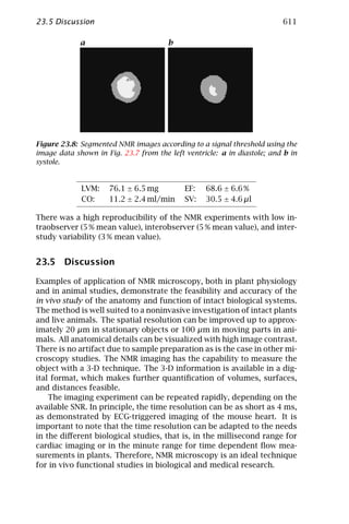


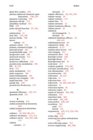


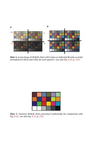


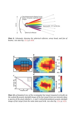

Computer vision handbook of computer vision and applications volume 1 - sensors and imaging
- 1. 1 1 2 2 1 1 2 4 2 4 2 2 1 1 2 2 1 1 HANDBOOK OF COMPUTER VISION AND APPLICATIONS Volume 1 Sensors and Imaging Bernd Jähne Horst Haußecker Peter Geißler ACADEMIC PRESS
- 2. Handbook of Computer Vision and Applications Volume 1 Sensors and Imaging
- 4. Handbook of Computer Vision and Applications Volume 1 Sensors and Imaging Editors Bernd Jähne Interdisciplinary Center for Scientific Computing University of Heidelberg, Heidelberg, Germany and Scripps Institution of Oceanography University of California, San Diego Horst Haußecker Peter Geißler Interdisciplinary Center for Scientific Computing University of Heidelberg, Heidelberg, Germany ACADEMIC PRESS San Diego London Boston New York Sydney Tokyo Toronto
- 5. This book is printed on acid-free paper. Copyright © 1999 by Academic Press. All rights reserved. No part of this publication may be reproduced or transmitted in any form or by any means, electronic or mechanical, including photocopy, recording, or any information storage and retrieval system, without permission in writing from the publisher. The appearance of code at the bottom of the first page of a chapter in this book indicates the Publisher’s consent that copies of the chapter may be made for personal or internal use of specific clients. This consent is given on the con- dition, however, that the copier pay the stated per-copy fee through the Copy- right Clearance Center, Inc. (222 Rosewood Drive, Danvers, Massachusetts 01923), for copying beyond that permitted by Sections 107 or 108 of the U.S. Copyright Law. This consent does not extend to other kinds of copying, such as copying for general distribution, for advertising or promotional purposes, for creating new collective works, or for resale. Copy fees for pre-1999 chap- ters are as shown on the title pages; if no fee code appears on the title page, the copy fee is the same as for current chapters. ISBN 0-12-379770-5/$30.00 ACADEMIC PRESS A Division of Harcourt Brace & Company 525 B Street, Suite 1900, San Diego, CA 92101-4495 http://www.apnet.com ACADEMIC PRESS 24-28 Oval Road, London NW1 7DX, UK http://www.hbuk.co.uk/ap/ Library of Congress Cataloging-In-Publication Data Handbook of computer vision and applications / edited by Bernd Jähne, Horst Haussecker, Peter Geissler. p. cm. Includes bibliographical references and indexes. Contents: v. 1. Sensors and imaging — v. 2. Signal processing and pattern recognition — v. 3. Systems and applications. ISBN 0–12–379770–5 (set). — ISBN 0–12–379771-3 (v. 1) ISBN 0–12–379772–1 (v. 2). — ISBN 0–12–379773-X (v. 3) 1. Computer vision — Handbooks, manuals. etc. I. Jähne, Bernd 1953– . II. Haussecker, Horst, 1968– . III. Geissler, Peter, 1966– . TA1634.H36 1999 006.3 7 — dc21 98–42541 CIP Printed in the United States of America 99 00 01 02 03 DS 9 8 7 6 5 4 3 2 1
- 6. Contents Preface xi Contributors xiii 1 Introduction 1 B. Jähne 1.1 Components of a vision system . . . . . . . . . . . . . . . . . . . 1 1.2 Imaging systems . . . . . . . . . . . . . . . . . . . . . . . . . . . . . 2 I Illumination and Image Formation 2 Radiation 7 H. Haußecker 2.1 Introduction . . . . . . . . . . . . . . . . . . . . . . . . . . . . . . . . 8 2.2 Fundamentals of electromagnetic radiation . . . . . . . . . . . . 9 2.3 Radiometric quantities . . . . . . . . . . . . . . . . . . . . . . . . . 13 2.4 Fundamental concepts of photometry . . . . . . . . . . . . . . . 24 2.5 Thermal emission of radiation . . . . . . . . . . . . . . . . . . . . 28 2.6 Acoustic waves . . . . . . . . . . . . . . . . . . . . . . . . . . . . . . 34 2.7 References . . . . . . . . . . . . . . . . . . . . . . . . . . . . . . . . . 35 3 Interaction of Radiation with Matter 37 H. Haußecker 3.1 Introduction . . . . . . . . . . . . . . . . . . . . . . . . . . . . . . . . 37 3.2 Basic definitions and terminology . . . . . . . . . . . . . . . . . . 39 3.3 Properties related to interfaces and surfaces . . . . . . . . . . . 43 3.4 Bulk-related properties of objects . . . . . . . . . . . . . . . . . . 52 3.5 References . . . . . . . . . . . . . . . . . . . . . . . . . . . . . . . . . 61 4 Imaging Optics 63 P. Geißler 4.1 Introduction . . . . . . . . . . . . . . . . . . . . . . . . . . . . . . . . 64 4.2 Basic concepts of geometric optics . . . . . . . . . . . . . . . . . 64 4.3 Lenses . . . . . . . . . . . . . . . . . . . . . . . . . . . . . . . . . . . . 67 4.4 Optical properties of glasses and other materials . . . . . . . . 78 4.5 Aberrations . . . . . . . . . . . . . . . . . . . . . . . . . . . . . . . . 81 4.6 Optical image formation . . . . . . . . . . . . . . . . . . . . . . . . 90 4.7 Wave and Fourier optics . . . . . . . . . . . . . . . . . . . . . . . . 96 4.8 References . . . . . . . . . . . . . . . . . . . . . . . . . . . . . . . . . 101 v
- 7. vi Contents 5 Radiometry of Imaging 103 H. Haußecker 5.1 Introduction . . . . . . . . . . . . . . . . . . . . . . . . . . . . . . . . 104 5.2 Observing surfaces . . . . . . . . . . . . . . . . . . . . . . . . . . . . 104 5.3 Propagating radiance . . . . . . . . . . . . . . . . . . . . . . . . . . 112 5.4 Radiance of imaging . . . . . . . . . . . . . . . . . . . . . . . . . . . 115 5.5 Detecting radiance . . . . . . . . . . . . . . . . . . . . . . . . . . . . 118 5.6 Concluding summary . . . . . . . . . . . . . . . . . . . . . . . . . . 134 5.7 References . . . . . . . . . . . . . . . . . . . . . . . . . . . . . . . . . 135 6 Illumination Sources and Techniques 137 H. Haußecker 6.1 Introduction . . . . . . . . . . . . . . . . . . . . . . . . . . . . . . . . 137 6.2 Natural illumination . . . . . . . . . . . . . . . . . . . . . . . . . . . 138 6.3 Artificial illumination sources . . . . . . . . . . . . . . . . . . . . . 141 6.4 Illumination setups . . . . . . . . . . . . . . . . . . . . . . . . . . . 157 6.5 References . . . . . . . . . . . . . . . . . . . . . . . . . . . . . . . . . 162 II Imaging Sensors 7 Solid-State Image Sensing 165 P. Seitz 7.1 Introduction . . . . . . . . . . . . . . . . . . . . . . . . . . . . . . . . 166 7.2 Fundamentals of solid-state photosensing . . . . . . . . . . . . 168 7.3 Photocurrent processing . . . . . . . . . . . . . . . . . . . . . . . . 175 7.4 Transportation of photosignals . . . . . . . . . . . . . . . . . . . . 182 7.5 Electronic signal detection . . . . . . . . . . . . . . . . . . . . . . . 185 7.6 Architectures of image sensors . . . . . . . . . . . . . . . . . . . . 189 7.7 Camera and video standards . . . . . . . . . . . . . . . . . . . . . 194 7.8 Semiconductor technology for image sensing . . . . . . . . . . 204 7.9 Practical limitations of semiconductor photosensors . . . . . . 207 7.10 The future of image sensing . . . . . . . . . . . . . . . . . . . . . . 209 7.11 Conclusions . . . . . . . . . . . . . . . . . . . . . . . . . . . . . . . . 218 7.12 References . . . . . . . . . . . . . . . . . . . . . . . . . . . . . . . . . 219 8 HDRC-Imagers for Natural Visual Perception 223 U. Seger, U. Apel, and B. Höfflinger 8.1 Introduction . . . . . . . . . . . . . . . . . . . . . . . . . . . . . . . . 223 8.2 Log compression at the pixel site . . . . . . . . . . . . . . . . . . 224 8.3 Random pixel access . . . . . . . . . . . . . . . . . . . . . . . . . . 228 8.4 Optimized SNR by bandwidth control per pixel . . . . . . . . . 228 8.5 Data density in the log space . . . . . . . . . . . . . . . . . . . . . 230 8.6 Color constancy in the log space . . . . . . . . . . . . . . . . . . . 230 8.7 Development of functionality and spatial resolution . . . . . . 231 8.8 References . . . . . . . . . . . . . . . . . . . . . . . . . . . . . . . . . 235 9 Image Sensors in TFA (Thin Film on ASIC) Technology 237 B. Schneider, P. Rieve, and M. Böhm 9.1 Introduction . . . . . . . . . . . . . . . . . . . . . . . . . . . . . . . . 238 9.2 Thin-film detectors . . . . . . . . . . . . . . . . . . . . . . . . . . . . 239
- 8. Contents vii 9.3 TFA properties and design considerations . . . . . . . . . . . . 249 9.4 TFA array prototypes . . . . . . . . . . . . . . . . . . . . . . . . . . 256 9.5 TFA array concepts . . . . . . . . . . . . . . . . . . . . . . . . . . . 262 9.6 Conclusions . . . . . . . . . . . . . . . . . . . . . . . . . . . . . . . . 267 9.7 References . . . . . . . . . . . . . . . . . . . . . . . . . . . . . . . . . 268 10 Poly SiGe Bolometers 271 S. Sedky and P. Fiorini 10.1 Overview . . . . . . . . . . . . . . . . . . . . . . . . . . . . . . . . . . 272 10.2 Principle of operation of bolometers . . . . . . . . . . . . . . . . 274 10.3 Microbolometer focal plane arrays . . . . . . . . . . . . . . . . . . 280 10.4 Bolometer materials . . . . . . . . . . . . . . . . . . . . . . . . . . . 284 10.5 Poly SiGe bolometers . . . . . . . . . . . . . . . . . . . . . . . . . . 288 10.6 Characterization of poly SiGe bolometers . . . . . . . . . . . . . 292 10.7 Conclusions . . . . . . . . . . . . . . . . . . . . . . . . . . . . . . . . 302 10.8 References . . . . . . . . . . . . . . . . . . . . . . . . . . . . . . . . . 303 11 Hyperspectral and Color Imaging 309 B. Jähne 11.1 Spectral signatures . . . . . . . . . . . . . . . . . . . . . . . . . . . . 309 11.2 Spectral sampling methods . . . . . . . . . . . . . . . . . . . . . . 310 11.3 Human color vision . . . . . . . . . . . . . . . . . . . . . . . . . . . 315 11.4 References . . . . . . . . . . . . . . . . . . . . . . . . . . . . . . . . . 320 III Two-Dimensional Imaging 12 Dynamic Fluorescence Imaging 323 D. Uttenweiler and R. H. A. Fink 12.1 Introduction . . . . . . . . . . . . . . . . . . . . . . . . . . . . . . . . 323 12.2 Fluorescence . . . . . . . . . . . . . . . . . . . . . . . . . . . . . . . . 324 12.3 Fluorescent indicators . . . . . . . . . . . . . . . . . . . . . . . . . 328 12.4 Microscopic techniques . . . . . . . . . . . . . . . . . . . . . . . . . 332 12.5 Analysis of fluorescence images . . . . . . . . . . . . . . . . . . . 342 12.6 Summary . . . . . . . . . . . . . . . . . . . . . . . . . . . . . . . . . . 343 12.7 References . . . . . . . . . . . . . . . . . . . . . . . . . . . . . . . . . 344 13 Electron Microscopic Image Acquisition 347 H. Stegmann, R. Wepf, and R. R. Schröder 13.1 Introduction . . . . . . . . . . . . . . . . . . . . . . . . . . . . . . . . 348 13.2 Electron-specimen interactions . . . . . . . . . . . . . . . . . . . . 349 13.3 Transmission electron microscopy (TEM) . . . . . . . . . . . . . 350 13.4 Scanning transmission electron microscopy (STEM) . . . . . . . 359 13.5 Analytical transmission electron microscopy . . . . . . . . . . . 361 13.6 Scanning electron microscopy (SEM) . . . . . . . . . . . . . . . . 364 13.7 Preparation techniques . . . . . . . . . . . . . . . . . . . . . . . . . 368 13.8 Digital image processing of electron micrographs . . . . . . . . 369 13.9 Imaging examples . . . . . . . . . . . . . . . . . . . . . . . . . . . . 370 13.10 References . . . . . . . . . . . . . . . . . . . . . . . . . . . . . . . . . 383
- 9. viii Contents 14 Processing of Ultrasound Images in Medical Diagnosis 387 W. Albert and M. Pandit 14.1 Introduction . . . . . . . . . . . . . . . . . . . . . . . . . . . . . . . . 387 14.2 Ultrasound imaging systems . . . . . . . . . . . . . . . . . . . . . 390 14.3 Processing the B-mode image . . . . . . . . . . . . . . . . . . . . . 399 14.4 Examples of image processing of B-mode images . . . . . . . . 404 14.5 Conclusions and perspectives . . . . . . . . . . . . . . . . . . . . . 411 14.6 References . . . . . . . . . . . . . . . . . . . . . . . . . . . . . . . . . 412 15 Acoustic Daylight Imaging in the Ocean 415 M. J. Buckingham 15.1 Introduction . . . . . . . . . . . . . . . . . . . . . . . . . . . . . . . . 415 15.2 The pilot experiment . . . . . . . . . . . . . . . . . . . . . . . . . . 416 15.3 ADONIS . . . . . . . . . . . . . . . . . . . . . . . . . . . . . . . . . . . 418 15.4 Acoustic daylight images . . . . . . . . . . . . . . . . . . . . . . . . 420 15.5 Concluding remarks . . . . . . . . . . . . . . . . . . . . . . . . . . . 422 15.6 References . . . . . . . . . . . . . . . . . . . . . . . . . . . . . . . . . 423 16 The Multisensorial Camera for Industrial Vision Applications 425 R. Massen 16.1 Image segmentation with little robustness . . . . . . . . . . . . 425 16.2 Sensor fusion and multisensorial camera . . . . . . . . . . . . . 426 16.3 A feature vector with every pixel . . . . . . . . . . . . . . . . . . . 428 16.4 A real-time three-dimensional linescan camera . . . . . . . . . 429 16.5 A real-time linescan scatter camera . . . . . . . . . . . . . . . . . 430 16.6 The multisensorial color-height-scatter camera . . . . . . . . . 433 16.7 Compressing the multisensorial camera signals . . . . . . . . . 435 16.8 The one-chip multisensorial camera . . . . . . . . . . . . . . . . . 435 16.9 Conclusion . . . . . . . . . . . . . . . . . . . . . . . . . . . . . . . . . 436 16.10 References . . . . . . . . . . . . . . . . . . . . . . . . . . . . . . . . . 437 IV Three-Dimensional Imaging 17 Geometric Calibration of Digital Imaging Systems 441 R. Godding 17.1 Definitions . . . . . . . . . . . . . . . . . . . . . . . . . . . . . . . . . 442 17.2 Parameters influencing geometrical performance . . . . . . . . 442 17.3 Model of image formation with the aid of optical systems . . 444 17.4 Camera models . . . . . . . . . . . . . . . . . . . . . . . . . . . . . . 445 17.5 Calibration and orientation techniques . . . . . . . . . . . . . . . 450 17.6 Photogrammetric applications . . . . . . . . . . . . . . . . . . . . 457 17.7 References . . . . . . . . . . . . . . . . . . . . . . . . . . . . . . . . . 460 18 Principles of Three-Dimensional Imaging Techniques 463 R. Schwarte, H. Heinol, B. Buxbaum, T. Ringbeck, Z. Xu, and K. Hartmann 18.1 Introduction . . . . . . . . . . . . . . . . . . . . . . . . . . . . . . . . 464 18.2 Basic principles . . . . . . . . . . . . . . . . . . . . . . . . . . . . . . 465 18.3 Some criteria and specifications . . . . . . . . . . . . . . . . . . . 467 18.4 Triangulation . . . . . . . . . . . . . . . . . . . . . . . . . . . . . . . 469 18.5 Time-of-flight (TOF) of modulated light . . . . . . . . . . . . . . 474
- 10. Contents ix 18.6 Optical Interferometry (OF) . . . . . . . . . . . . . . . . . . . . . . 479 18.7 Outlook . . . . . . . . . . . . . . . . . . . . . . . . . . . . . . . . . . . 482 18.8 References . . . . . . . . . . . . . . . . . . . . . . . . . . . . . . . . . 482 19 Three-Dimensional Sensors—Potentials and Limitations 485 G. Häusler 19.1 Introduction . . . . . . . . . . . . . . . . . . . . . . . . . . . . . . . . 485 19.2 Why three-dimensional sensors? . . . . . . . . . . . . . . . . . . . 486 19.3 Some important questions about three-dimensional sensing . 488 19.4 Triangulation on optically rough surfaces . . . . . . . . . . . . . 489 19.5 White-light interferometry on rough surfaces . . . . . . . . . . 495 19.6 Summary . . . . . . . . . . . . . . . . . . . . . . . . . . . . . . . . . . 503 19.7 Conclusion . . . . . . . . . . . . . . . . . . . . . . . . . . . . . . . . . 504 19.8 References . . . . . . . . . . . . . . . . . . . . . . . . . . . . . . . . . 505 20 High-Performance Surface Measurement 507 R. W. Malz 20.1 Introduction . . . . . . . . . . . . . . . . . . . . . . . . . . . . . . . . 508 20.2 Close-range photogrammetry . . . . . . . . . . . . . . . . . . . . . 511 20.3 Sequential light processing and information theory . . . . . . 517 20.4 Advanced self-calibration of three-dimensional sensors . . . . 526 20.5 Hybrid navigation of three-dimensional sensors . . . . . . . . . 529 20.6 Mobile measuring system “Ganymed” . . . . . . . . . . . . . . . 532 20.7 Conclusions . . . . . . . . . . . . . . . . . . . . . . . . . . . . . . . . 536 20.8 References . . . . . . . . . . . . . . . . . . . . . . . . . . . . . . . . . 538 21 Three-Dimensional Light Microscopy 541 E. H. K. Stelzer 21.1 Three-dimensional microscopy . . . . . . . . . . . . . . . . . . . . 542 21.2 Telecentricity . . . . . . . . . . . . . . . . . . . . . . . . . . . . . . . 543 21.3 Theory of three-dimensional imaging . . . . . . . . . . . . . . . . 547 21.4 Confocal microscopy . . . . . . . . . . . . . . . . . . . . . . . . . . 548 21.5 Index mismatching effects . . . . . . . . . . . . . . . . . . . . . . . 555 21.6 Developments in confocal microscopy . . . . . . . . . . . . . . . 556 21.7 Resolution versus distance . . . . . . . . . . . . . . . . . . . . . . 557 21.8 Perspectives of three-dimensional light microscope . . . . . . 558 21.9 References . . . . . . . . . . . . . . . . . . . . . . . . . . . . . . . . . 559 22 Magnetic Resonance Imaging in Medicine 563 W. G. Schreiber and G. Brix 22.1 Introduction . . . . . . . . . . . . . . . . . . . . . . . . . . . . . . . . 564 22.2 Basic magnetic resonance physics . . . . . . . . . . . . . . . . . . 564 22.3 Image acquisition and reconstruction . . . . . . . . . . . . . . . . 574 22.4 Image contrast . . . . . . . . . . . . . . . . . . . . . . . . . . . . . . 587 22.5 Fast imaging methods . . . . . . . . . . . . . . . . . . . . . . . . . . 591 22.6 Overview of quantitative applications . . . . . . . . . . . . . . . 596 22.7 References . . . . . . . . . . . . . . . . . . . . . . . . . . . . . . . . . 598
- 11. x Contents 23 Nuclear Magnetic Resonance Microscopy 601 A. Haase, J. Ruff, and M. Rokitta 23.1 Introduction . . . . . . . . . . . . . . . . . . . . . . . . . . . . . . . . 601 23.2 Methodology . . . . . . . . . . . . . . . . . . . . . . . . . . . . . . . . 603 23.3 Applications to plant studies . . . . . . . . . . . . . . . . . . . . . 605 23.4 Applications to animal studies . . . . . . . . . . . . . . . . . . . . 609 23.5 Discussion . . . . . . . . . . . . . . . . . . . . . . . . . . . . . . . . . 611 23.6 References . . . . . . . . . . . . . . . . . . . . . . . . . . . . . . . . . 612 Index 613
- 12. Preface What this handbook is about This handbook offers a fresh approach to computer vision. The whole vision process from image formation to measuring, recognition, or re- acting is regarded as an integral process. Computer vision is under- stood as the host of techniques to acquire, process, analyze, and un- derstand complex higher-dimensional data from our environment for scientific and technical exploration. In this sense the handbook takes into account the interdisciplinary nature of computer vision with its links to virtually all natural sciences and attempts to bridge two important gaps. The first is between mod- ern physical sciences and the many novel techniques to acquire images. The second is between basic research and applications. When a reader with a background in one of the fields related to computer vision feels he has learned something from one of the many other facets of com- puter vision, the handbook will have fulfilled its purpose. The handbook comprises three volumes. The first volume, Sensors and Imaging, covers image formation and acquisition. The second vol- ume, Signal Processing and Pattern Recognition, focuses on processing of the spatial and spatiotemporal signal acquired by imaging sensors. The third volume, Systems and Applications, describes how computer vision is integrated into systems and applications. Prerequisites It is assumed that the reader is familiar with elementary mathematical concepts commonly used in computer vision and in many other areas of natural sciences and technical disciplines. This includes the basics of set theory, matrix algebra, differential and integral equations, com- plex numbers, Fourier transform, probability, random variables, and graphing. Wherever possible, mathematical topics are described intu- itively. In this respect it is very helpful that complex mathematical relations can often be visualized intuitively by images. For a more for- xi
- 13. xii Preface mal treatment of the corresponding subject including proofs, suitable references are given. How to use this handbook The handbook has been designed to cover the different needs of its readership. First, it is suitable for sequential reading. In this way the reader gets an up-to-date account of the state of computer vision. It is presented in a way that makes it accessible for readers with different backgrounds. Second, the reader can look up specific topics of inter- est. The individual chapters are written in a self-consistent way with extensive cross-referencing to other chapters of the handbook and ex- ternal references. The CD that accompanies each volume of the hand- book contains the complete text of the handbook in the Adobe Acrobat portable document file format (PDF). This format can be read on all major platforms. Free Acrobat reader version 3.01 for all major com- puting platforms is included on the CDs. The texts are hyperlinked in multiple ways. Thus the reader can collect the information of interest with ease. Third, the reader can delve more deeply into a subject with the material on the CDs. They contain additional reference material, interactive software components, code examples, image material, and references to sources on the Internet. For more details see the readme file on the CDs. Acknowledgments Writing a handbook on computer vision with this breadth of topics is a major undertaking that can succeed only in a coordinated effort that involves many co-workers. Thus the editors would like to thank first all contributors who were willing to participate in this effort. Their cooperation with the constrained time schedule made it possible that the three-volume handbook could be published in such a short period following the call for contributions in December 1997. The editors are deeply grateful for the dedicated and professional work of the staff at AEON Verlag & Studio who did most of the editorial work. We also express our sincere thanks to Academic Press for the opportunity to write this handbook and for all professional advice. Last but not least, we encourage the reader to send us any hints on errors, omissions, typing errors, or any other shortcomings of the handbook. Actual information about the handbook can be found at the editors homepage http://klimt.iwr.uni-heidelberg.de. Heidelberg, Germany and La Jolla, California, December 1998 Bernd Jähne, Horst Haußecker, Peter Geißler
- 14. Contributors Werner F. Albert studied medicine at the Universities of Saarland and Cologne. He obtained the degree of Doc- tor of Medicine in 1970 and completed the Habilitation in 1981 at the University of Saarland. Since 1983 he has been Chief Physician of the Department of Internal Medicine of the Westpfalz-Klinikum Kaiserslautern and since 1991 its Medical Director. He has been an Adjunct Professor at the University of Saarland at Homburg since 1986. His current research interests include transplan- tation medicine and gastroenterology. Prof. Dr. Werner F. Albert, Medizinische Klinik III Westpfalz-Klinikum, D-67653 Kaiserslautern, Germany Uwe Apel received his diploma degree in Physics at the University of Gießen in 1984. From 1984 to 1987 he was engaged as a process engineer at the power semi- conductor facility of Robert Bosch GmbH at Reutlingen. In 1987 he changed to the Institute for Microelectronics in Stuttgart. In 1994 he joined the image sensor design team. He has made major contributions to several pend- ing patents in circuit design and camera system related topics. Uwe Apel, Institute for Microelectronics, Stuttgart Allmandring 30a, D-70569 Stuttgart, Germany apel@www.ims-chips.de Markus Böhm received the Dipl.-Ing. and the Dr.-Ing. de- grees in electrical engineering from the Technical Univer- sity, Berlin, Germany, in 1979 and 1983, respectively. In 1984/85, he was a visiting scientist with the Department of Electrical Engineering of the University of Delaware. In 1985, he joined Chronar Corporation in Princeton, New Jersey. Since 1989 he has been a Professor at the Univer- sity of Siegen, Germany, where he heads the Institute for Semiconductor Electronics. His research interests focus on thin-film technology, novel imaging devices and pho- tovoltaics. He is a co-founder of Silicon Vision GmbH. Prof. Markus Böhm, Institut für Halbleiterelektronik (IHE) Universität-GH Siegen, Hölderlinstr. 3, D-57068 Siegen, Germany boehm@teb.et-inf.uni-siegen.de, www.uni-siegen.de/˜ihe/ xiii
- 15. xiv Contributors Michael J. Buckingham is Professor of Ocean Acoustics at Scripps Institution of Oceanography. His research in- terests include imaging in the ocean, marine sediments, and sea-surface processes. He is a Fellow of the Acous- tical Society of America, the Institute of Acoustics, the Institute of Electrical Engineers, and the Explorers Club, and a member of the New York Academy of Sciences. In 1982 he received the A. B. Wood Medal from the IOA and he is the recipient of many other awards. Prof. Michael J. Buckingham Marine Physical Laboratory Scripps Institution of Oceanography University of California, San Diego 9500 Gilman Drive, La Jolla, CA 92093-0213, USA, mjb@mpl.ucsd.edu, Gunnar Brix studied physics in Karlsruhe and Heidel- berg. In 1985 he received his diploma degree from the University of Karlsruhe and in 1989 a doctoral degree from the University of Heidelberg. From 1994 to 1998 he was assistant professor for medical physics at the University of Heidelberg where he headed the depart- ment of biophysics and medical radiation physics at the German Cancer Research Center in Heidelberg. His cur- rent research interests include the development of new magnetic resonance imaging (MRI) and positron emis- sion tomography (PET) data acquisition techniques as well as the analysis of kinetic data within the framework of kinetic modeling. Priv.-Doz. Dr. Gunnar Brix Abteilung Medizinische Strahlenhygiene und nichtionisierende Strahlung Bundesamt für Strahlenschutz, Postfach 10 01 49 D-38201 Salzgitter, Germany Paolo Fiorini took his degree in Solid State Physics at the University of Rome in 1977; his thesis was on exi- tons in silicon. He has been active in the field of electri- cal and optical properties of semiconductors for many years, working at the University of Rome, Strasbourg (France), IBM Research Center in Yorktown Heights, NY (USA) and at the Interuniversity Microelectronic Center (IMEC) in Leuven (Belgium). At present, he is associate professor, Physics Department of the Third University of Rome. Prof. Paolo Fiorini, Dept. of Physics 3rd University of Rome, Via della Vasca Navale 86, I-00156 Rome, Italy
- 16. Contributors xv Rainer H.A. Fink is a professor at the II. Institute of Phys- iology at the University of Heidelberg. His research inter- ests comprise calcium regulation, activation of contrac- tile force, membrane electrophysiology, and laser appli- cations in the biophysics of muscular contraction. He held research and teaching positions at the University of Washington, Seattle, WA, U.S., La Trobe University, Mel- bourne, and the University of Adelaide, Australia, before taking up his professorship in Heidelberg in 1990. He received his PhD in 1979 at the University of Bochum, Germany. Prof. Dr. Rainer H.A. Fink, II. Physiologisches Institut Universität Heidelberg, Im Neuenheimer Feld 326 D-69120 Heidelberg, Germany fink@novsrv1.pio1.uni-heidelberg.de Peter Geißler studied physics in Heidelberg. He received his diploma and doctoral degree from Heidelberg Uni- versity in 1994 and 1998, respectively. His research in- terests include computer vision, especially depth-from- focus, adaptive filtering, and flow visualization as well as the application of image processing in physical sciences and oceanography. Dr. Peter Geißler Forschungsgruppe Bildverarbeitung, IWR Universität Heidelberg, Im Neuenheimer Feld 368 D-69120 Heidelberg, Germany Peter.Geissler@iwr.uni-heidelberg.de http://klimt.iwr.uni-heidelberg.de Robert Godding received his diploma in geodesy from the University of Bonn in 1987. From 1987 to 1989 he worked as research scientist at the Institute for Pho- togrammetry at the University of Bonn and from 1989 to 1994 at the Institute for Photogrammetry and Image Processing at the University of Braunschweig in the field of close-range photogrammetry. From 1994 to 1998 he was with Rollei Fototechnic in Braunschweig, first re- sponsible for research and development of close-range photogrammetry systems, later as head of the RolleiMet- ric Department. Since December 1998 he has been with AICON GmbH in Braunschweig. His main interests are close range-digital photogrammetry in industrial applications and the use of high-resolution digital cameras for optical measurement techniques. Robert Godding AICON GmbH, Celler Straße 32, D-38114 Braunschweig, Germany robert.godding@aicon.de, http://www.aicon.de
- 17. xvi Contributors Hermann Gröning graduated in 1996 from the Univer- sity of Heidelberg with a master degree in physics and is now pursuing his PhD at the Interdisciplinary Center for Scientific Computing. He is concerned mainly with radiometric and geometric camera calibration. Hermann Gröning Forschungsgruppe Bildverarbeitung, IWR Universität Heidelberg Im Neuenheimer Feld 368 D-69120 Heidelberg, Germany Hermann.Groening@iwr.uni-heidelberg.de Axel Haase studied physics at the universities of Erlan- gen and Gießen. He received his diploma from the Uni- versity of Gießen in 1977 and a doctoral degree in 1980. During his doctoral work and later in postdoctoral work, he worked at the Max-Planck-Institut für biophysikalis- che Chemie in Göttingen. In 1981 he spent one postdoc- toral year at the Biochemistry Department of the Univer- sity of Oxford, UK, with Prof. G. K. Radda. He worked as a scientist at the Max-Planck-Institut für biophysikalische Chemie until 1989. During this period he invented fast NMR imaging (FLASH) and other NMR techniques (CHESS imaging, STEAM imaging). He received his habilitation from the University of Frankfurt in 1987. Since 1989, he has held the chair of biophysics at the Uni- versity of Würzburg. Prof. Dr. Axel Haase, Physikalisches Institut, Universität Würzburg Am Hubland, D-97074 Würzburg, Germany haase@physik.uni-wuerzburg.de Gerd Häusler is adjunct professor, University of Erlan- gen, Chair for Optics, and director of the Optical Metrol- ogy Group. He received his diploma in 1970 and a doc- toral degree in 1974 from the Optical Institute, Techni- cal University Berlin. In 1974 he moved to the Chair for Applied Optics (later Chair for Optics), University of Er- langen. There he received his habilitation in 1982. As a doctoral fellow he worked with IBM (Sindelfingen), ENST Telecom (Paris), and RCA (Zürich). At the University of Munich and the RIKEN Institute in Tokyo he worked on optical and electronical image processing and nonlinear optical feedback systems. His current research interests include the investigation of the physical limits of range sensing and the con- struction of sensors that work at these limits and cover the nanometer to meter range, with applications in industry and medicine. Prof. Dr. Gerd Häusler, Chair for Optics, Universität Erlangen-Nürnberg Staudtstraße 7/B2, D-91056 Erlangen, Germany haeusler@physik.uni-erlangen.de
- 18. Contributors xvii Horst Haußecker studied physics in Heidelberg. He re- ceived his diploma in physics and his doctoral degree from Heidelberg University in 1994 and 1996, respec- tively. He was visiting scientist at the Scripps Institution of Oceanography in 1994. Currently he is conducting research in the image processing research group at the Interdisciplinary Center for Scientific Computing (IWR), where he also lectures on optical flow computation. His research interests include computer vision, especially image sequence analysis, infrared thermography, and fuzzy-image processing, as well as the application of im- age processing in physical sciences and oceanography. Dr. Horst Haußecker, Forschungsgruppe Bildverarbeitung, IWR Universität Heidelberg, Im Neuenheimer Feld 368, D-69120 Heidelberg Horst.Haussecker@iwr.uni-heidelberg.de http://klimt.iwr.uni-heidelberg.de Bernd Höfflinger received his Diploma in Physics in 1964 and his PhD in 1967. He was a member of the scientific staff of the Siemens Research Laboratory in Munich from 1964-1967. From 1967-1969 he was Assistant Profes- sor, School of Electrical Engineering, Cornell University, Ithaca, NY, USA. He was manager of the MOS Integrated Circuits Division of the Siemens Components Group in Munich from 1970-1972. He then founded the Depart- ment of Electrical Engineering at the University of Dort- mund. In 1981 he became Head of the Department of Electrical Engineering and Co-Director of the Microelec- tronics and Information Sciences Center at the University of Minnesota. Since September 1985 he has been Director and Chairman of the Board of the Institute for Microelectronics, Stuttgart. Prof. Dr. Bernd Höfflinger, Institute for Microelectronics Stuttgart (IMS) Allmandring 30a, D-70569 Stuttgart, Germany E-mail: hoefflinger@www.ims-chips.de Bernd Jähne studied physics in Saarbrücken and Hei- delberg. He received his diploma, doctoral degree, and habilitation degree from Heidelberg University in 1977, 1980, and 1985, respectively, and a habilitation de- gree in applied computer science from the University of Hamburg-Harburg in 1992. Since 1988 he has been a Ma- rine Research Physicist at Scripps Institution of Oceanog- raphy, University of California, and, since 1994, he has been professor of physics at the Interdisciplinary Center of Scientific Computing. He leads the research group on image processing. His research interests include com- puter vision, especially filter design and image sequence analysis, the application of image processing techniques in science and industry, and small-scale air-sea interaction processes.
- 19. xviii Contributors Prof. Dr. Bernd Jähne, Forschungsgruppe Bildverarbeitung, IWR Universität Heidelberg, Im Neuenheimer Feld 368, D-69120 Heidelberg Bernd.Jaehne@iwr.uni-heidelberg.de http://klimt.iwr.uni-heidelberg.de Reinhard Malz studied communication and computer science in Esslingen and electrical engineering in Stuttgart. He received diploma degrees in 1978 and 1984 and the doctoral degree from University of Stuttgart in 1992. His research interests include analog and digi- tal electronics, semiconductor physics, optics, pattern recognition, and active optical information processing for inspection and measurement. Currently he is a re- searcher at Daimler-Chrysler AG, where he develops 3-D measurement systems for reverse engineering and qual- ity control. Dr. Reinhard Malz, Daimler-Chrysler AG Wilhelm-Runge-Str. 11, D-89081 Ulm, Germany, Reinhard.Malz@t-online.de Robert Massen studied electronic communications at the University of Technology of Aachen, Germany. His PhD thesis covers stochastic computing, an early non-von Neumann computer architecture with random data cod- ing and massively parallel organization. In 1974, he became professor in the Department of Computer Sci- ence at the Fachhochschule (University of Applied Sci- ences) Konstanz. He has been active in industrial im- age processing since 1984, first as director of the for- profit Steinbeis Transfer Center for Image Processing. In 1992, he founded the MASSEN machine vision systems GmbH, Konstanz, through a management buy-out. The company is a major German supplier of advanced dedicated color vision systems for on-line monitoring of surfaces and for real-time sortation. Prof. Dr. Ing. Robert Massen, MASSEN machine vision systems GmbH Lohnerhofstrasse 2, D-78467 Konstanz, Germany, Robert.Massen@t-online.de Madhukar Pandit studied electrical engineering in Ban- galore and Karlsruhe. He obtained the Dr.-Ing. degree in Control Systems in the Technische Hochschule Karlsruhe and the Habilitation in the Kaiserslautern University. He worked at the National Aeronautical Laboratory, Banga- lore, Brown Boveri and Cie in Mannheim. Since 1978, he has been professor of Control Systems and Signal The- ory at the Kaiserslautern University. His group is active mainly in the areas of process control and image pro- cessing applied to medical imaging and quality control. Prof. Dr.-Ing. Madhukar Pandit, Lehrstuhl für Regelungstechnik und Signalthe- orie, Fachbereich Elektrotechnik, Universität Kaiserslautern Postfach 3049, D-67653 Kaiserslautern, Germany Pandit@e-technik.uni-kl.de, http://www.uni-kl.de/AG-Pandit/
- 20. Contributors xix Peter Rieve received the Dipl.-Ing. degree in electrical engineering from the University of Siegen, Germany, in 1994. From 1994 to 1997 he was a research engineer at the Institute for Semiconductor Electronics, University of Siegen. He worked in the field of sensor technolo- gies and focused on the development and optimization of amorphous silicon based black and white and color de- tectors for applications in image sensor systems in TFA technology. P. Rieve is now with Silicon Vision GmbH, Siegen. Peter Rieve, Silicon Vision GmbH Birlenbacher Str. 18, D-57078 Siegen, Germany rieve@siliconvision.de, http://www.siliconvision.de Markus Rokitta studied physics at the University of Würzburg. He received his diploma from the Univer- sity of Würzburg in 1994. Since 1996 he has been working for his doctoral degree in the area of NMR mi- croscopy applied to plant systems. He is member of the Graduiertenkolleg “Magnetische Kernresonanz in vivo und in vitro für die biologische und medizinische Grund- lagenforschung.” Dipl. Phys. Markus Rokitta Physikalisches Institut Universität Würzburg Am Hubland, D-97074 Würzburg, Germany Jan Ruff studied physics at the University of Würzburg. He received his diploma from the University of Würzburg in 1995. Since 1996 he has been working for his doc- toral degree in the area of NMR microscopy applied to animal studies. He is member of the Graduiertenkolleg “Magnetische Kernresonanz in vivo und in vitro für die biologische und medizinische Grundlagenforschung.” Dipl. Phys. Jan Ruff Physikalisches Institut Universität Würzburg Am Hubland, D-97074 Würzburg, Germany
- 21. xx Contributors Bernd Schneider received the Dipl.-Ing. degree in electri- cal engineering from the University of Siegen, Germany, in 1995. In the same year, he joined the Institute for Semiconductor Electronics at the University of Siegen. He works in the field of sensor technologies and focuses on the design, fabrication and characterization of ASICs for TFA image sensors. He is currently engaged in the development of new types of TFA sensor systems. Bernd Schneider, Institut für Halbleiterelektronik (IHE) Universität-GH Siegen Hölderlinstr. 3, D-57068 Siegen, Germany bernd s@teb.et-inf.uni-siegen.de http://www.uni-siegen.de/˜ihe/ Wolfgang Schreiber studied physics in Munich. He re- ceived his diploma from the University of Munich in 1990 and in 1994 a doctoral degree from the University of Hei- delberg. From 1994 to 1997 he was a postdoctoral fellow at the department of biophysics and medical radiation physics at the German Cancer Research Center in Hei- delberg. Since 1997 he has been head of the research group MR physics at the University of Mainz. His cur- rent research interests include the development of tech- niques for noninvasive assessment of physiology and pathophysiology by magnetic resonance imaging, pulse sequence development for ultrafast proton- and non-proton MRI in the brain, heart, and lung, and MRI data postprocessing techniques. Dr. Wolfgang Schreiber, Department of Radiology Johannes Gutenberg-University, Langenbeckstr. 1 D-55131 Mainz, Germany Wolfgang.Schreiber@radiologie.klinik.uni-mainz.de Rasmus R. Schröder studied physics and biology at the Ruprechts-Karls-Universität Heidelberg, Germany and at the Trinity College Dublin, Ireland. After receiving his PhD at Heidelberg University in theoretical elementary particle physics, he took up his biological interests by continuing his work in the department of Kenneth C. Holmes at the Max-Planck-Institut for medical research in Heidelberg. Here he started his work in electron mi- croscopy and image processing. Today he is group leader at the Max-Planck-Institut doing research on the image formation in energy filtered electron microscopes, quan- titative image processing, and investigating molecular structures of the muscle proteins actin and myosin in its force-producing interactions. Dr. Rasmus R. Schröder, MPI für medizinische Forschung Jahnstr. 29, D-69120 Heidelberg, Germany rasmus@mpimf-heidelberg.mpg.de
- 22. Contributors xxi Rudolf Schwarte studied electrical engineering at the RWTH Aachen. He received his diploma and doctoral de- gree from RWTH Aachen in 1965 and 1972. From 1973- 1978 he worked as the head research engineer at the In- stitute for Technical Electronics in Aachen, founded the company Sympuls GmbH in Aachen, followed by three years of leading research departments in several com- panies in Germany. Since 1981 he has been professor at the University of Siegen and head of the Institute for Data Processing (INV). He is the initiator and chair of the Center for Sensory Systems (ZESS) in Siegen. In 1995 he received the NRW innovation prize. He holds several patents in the fields of optical measurement and communication systems. In 1997 he founded S-TEC GmbH in Siegen. His main research interests include laser ranging systems, optical sensory systems, optical data communication, and digital signal processing. Prof. Dr. Rudolf Schwarte, Institut für Nachrichtenverarbeitung (INV) Universität-GH Siegen, Hölderlinstr. 3, D-57068 Siegen, Germany schwarte@nv.et-inf.uni-siegen.de http://www.nv.et-inf.uni-siegen.de/inv/inv.html Ulrich Seger received his diploma in electrical engineer- ing from the Fachhochschule Konstanz for his work on digital image preprocessing for optical character recognition in 1987. As design engineer in Computer Gesellschaft Konstanz mbHs R&D-department he was en- gaged in the development of a multiprocessor character recognition system. In 1989 he joint the Mikrosystems Division of the IMS, where he worked on chip and system design of CMOS microsystems involving optical sensors and analog signal processors and started the develop- ment of the first HDRC sensors. He is co-inventor of the basic HDRC principle and made major contributions to several pending patents in circuit design and camera system related topics. Ulrich Seger, Institute for Microelectronics Stuttgart Allmandring 30a, D-70569 Stuttgart, Germany seger@www.ims-chips.de Peter Seitz received his PhD degree in physics in 1984 from the Swiss Federal Institute of Technology (ETH) in Zürich, Switzerland. From 1984 to 1987 he was a staff member of the RCA research laboratories in Prince- ton, New Jersey and Zürich, Switzerland. Afterwards he transferred to the Swiss Paul Scherrer Institute. Since 1997 he has been working for the Swiss Center for Elec- tronics and Microtechnology (CSEM) in Neuchatel and Zürich, heading the Image Sensing Section in the Re- search division. Peter Seitz is the author of 90 publica- tions in the fields of applied optics, image sensing, ma- chine vision, and optical microsystems engineering, and he holds 8 patents.
- 23. xxii Contributors Prof. Dr. Peter Seitz Centre Suisse d’Electronique et de Microtechnique SA (CSEM) Badenerstrasse 569, CH-8048 Zurich, Switzerland peter.seitz@csem.ch, http://www.csem.ch/ Sherif Sedky graduated in 1992 from the department of Electrical and Communication Engineering of Cairo Uni- versity. In 1995 he obtained a master degree in Engi- neering Physics at the same university. In 1998 he was granted a PhD degree in micro electronics and material science from the Catholic University of Leuven (Belgium). He is active in the field of Sensors and Actuators. He is now a member of the microsystem technology group of the Interuniversity Microelectronics Center (IMEC) in Leuven (Belgium). He is also an assistant professor at the department of Engineering Physics, Faculty of Engineer- ing, Cairo University. Dr. Sherif Sedky Department of Engineering, Mathematics and Physics Faculty of Engineering, Cairo University, Giza, Egypt, sedky@imec.be E. H. K. Stelzer studied physics in Frankfurt am Main and in Heidelberg, Germany. During his Diploma thesis at the Max-Planck-Institut für Biophysik he worked on the physical chemistry of phospholipid vesicles, which he characterized by photon correlation spectroscopy. Since 1983 he has worked at the European Molecular Biol- ogy Laboratory (EMBL). He has contributed extensively to the development of confocal fluorescence microscopy and its application in life sciences. His group works on the development and application of high-resolution techniques in light microscopy, video microscopy, con- focal microscopy, optical tweezers, single particle analy- sis, and the documentation of relevant parameters with biological data. Prof. Dr. E. H. K. Stelzer, Light Microscopy Group, European Molecular Biology Laboratory (EMBL), Postfach 10 22 09 D-69120 Heidelberg, Germany, stelzer@EMBL-Heidelberg.de, Heiko Stegmann studied physics at the Ruprecht-Karls- Universität Heidelberg, Germany. He received his diplo- ma degree in 1996 and his PhD degree in 1998 from that university, working on analytical electron microscopy techniques for the investigation of muscle biophysics. At present he works on 3-D reconstruction of mo- tor molecules by cryo-electron microscopy at the Max- Planck-Institut for medical research in Heidelberg. Heiko Stegmann, MPI für medizinische Forschung Jahnstr. 29, D-69120 Heidelberg, Germany stegmann@mpimf-heidelberg.de
- 24. Contributors xxiii Dietmar Uttenweiler is a research fellow at the II. Insti- tute of Physiology at the University of Heidelberg in the group of Prof. Dr. R. H. A. Fink. He studied physics in Freiburg and Heidelberg. In 1990–1991 he worked at the University of Sussex, UK, supported by an Erasmus schol- arship. He graduated as Diplom-Physiker in 1994 and received his doctoral degree (Dr. rer. nat.) in physics in 1997 from the University of Heidelberg. His research interests in biophysics comprise fluorescence imaging techniques, mathematical modeling, and digital image processing, in particular for the study of motor proteins and the calcium regulation of force generation in muscle. Dr. Dietmar Uttenweiler, II. Physiologisches Institut University of Heidelberg, Im Neuenheimer Feld 326, D-69120 Heidelberg dietmar.uttenweiler@urz.uni-heidelberg.de Roger Wepf studied biology at the ETH, Swiss Federal Institute of Technology in Zurich, Switzerland, received his PhD at the Institute of Cell Biology, Swiss Federal In- stitute of Technology on surface imaging with high res- olution coating and worked as a postdoctoral fellow at the same institute on imaging of actin binding proteins, and at the EMBL, Heidelberg, Germany on new prepara- tion techniques for high-resolution LVSEM in the group of Max Haider. He then became a staff member in the junior-group Cryopreparation for EM and Cryo-SEM in the Cell Biology dept. at EMBL. At present he is the group leader of Electron Microscopy in the Central Analytical Dept. at Beiersdorf AG, Hamburg, Germany. Dr. Roger Wepf, Beiersdorf AG Unnastr. 48, D-20245 Hamburg, Germany wepf-r.ocp-65@bdfde86mhs.compuserve.com
- 25. xxiv Contributors
- 26. 1 Introduction Bernd Jähne Interdisziplinäres Zentrum für Wissenschaftliches Rechnen (IWR) Universität Heidelberg, Germany 1.1 Components of a vision system . . . . . . . . . . . . . . . . . . . 1 1.2 Imaging systems . . . . . . . . . . . . . . . . . . . . . . . . . . . . . 2 1.1 Components of a vision system Computer vision is a complex subject. As such it is helpful to divide it into the various components or function modules. On this level, it is also much easier to compare a technical system with a biological system. In this sense, the basic common functionality of biological and machine imaging includes the following components: Radiation source. If no radiation is emitted from the scene or the ob- ject of interest, nothing can be observed or processed. Thus appro- priate illumination is necessary for objects that are themselves not radiant. Camera. The “camera” collects the radiation received from the object in such a way that the radiation’s origins can be pinpointed. In the simplest case this is just an optical lens. But it could also be a completely different system, for example, an imaging optical spec- trometer, an x-ray tomograph, or a microwave dish. Sensor. The sensor converts the received radiative flux density into a suitable signal for further processing. For an imaging system nor- mally a 2-D array of sensors is required to capture the spatial dis- tribution of the radiation. With an appropriate scanning system in some cases a single sensor or a row of sensors could be sufficient. Processing unit. It processes the incoming, generally higher-dimen- sional data, extracting suitable features that can be used to measure object properties and categorize them into classes. Another impor- tant component is a memory system to collect and store knowl- edge about the scene, including mechanisms to delete unimportant things. 1 Handbook of Computer Vision and Applications Copyright © 1999 by Academic Press Volume 1 All rights of reproduction in any form reserved. Sensors and Imaging ISBN 0–12–379771–3/$30.00
- 27. 2 1 Introduction Property Radiance Irradiance Electric Digital Object signal ADC image Imaging Photo- radiation sampling system sensor s(x) interaction l(x) E(x) g(x) Gmn Figure 1.1: Chain of steps linking an object property to the signal measured by an imaging system. Actors. Actors react to the result of the visual observation. They be- come an integral part of the vision system when the vision system is actively responding to the observation by, for example, tracking an object of interest or by using a vision-guided navigation (active vision, perception action cycle). 1.2 Imaging systems Volume 1 of this handbook deals with imaging systems. It covers all processes involved in the formation of an image from objects and the sensors that convert radiation into electric signals. Generally the goal is to attain a signal from an object in such a form that we know where it is (geometry) and what it is or what properties it has. It is important to note that the type of answer we receive from these two implicit questions depends on the purpose of the vision system. The answer could be of qualitative or quantitative nature. For some ap- plications it could be sufficient to obtain a qualitative answer like “there is a car on the left coming towards you.” The “what” and “where” ques- tions can thus cover the entire range from “there is something,” a spec- ification of the object in the form of a class, to a detailed quantitative description of various properties of the objects of interest. The relation that links the object property to the signal measured by an imaging system is a complex chain of processes (Fig. 1.1). Interaction of the radiation with the object (possibly using an appropriate illumi- nation system) causes the object to emit radiation. A portion (usually only a very small part) of the emitted radiative energy is collected by the optical system and perceived as an irradiance (radiative energy/area). A sensor (or rather an array of sensors) converts the received radiation into an electrical signal that is subsequently sampled and digitized to form a digital image as an array of digital numbers. Only direct imaging systems provide a direct point to point corre- spondence between points of the objects in the 3-D world and at the image plane. Indirect imaging systems also give a spatially distributed irradiance but with no such one-to-one relation. Generation of an im- age requires reconstruction of the object from the perceived irradiance. Examples of such imaging techniques include radar imaging, various techniques for spectral imaging, acoustic imaging, tomographic imag- ing, and magnetic resonance imaging (Chapters 22 and 23).
- 28. 1.2 Imaging systems 3 The first part of this volume covers the basics of image formation (Chapters 2–6). The fundamentals of electromagnetic radiation, ra- diometry and photometry, and of thermal radiation are discussed in Chapter 2. Chapter 4 discusses basis knowledge regarding optics and optical systems, areas that are helpful to know for computer vision. Chapter 3 deals with the basic physical laws that determine the relation between object properties and the emitted radiation while Chapter 5 deals with the basic relations between the emitted radiation (radiance) and the received radiation at the sensor plane (irradiance). Chapter 6 covers two practical topics. First, it introduces various types of illu- mination sources that are available to illuminate a scene. Second, it describes the basic possibilities for illumination setups and their rela- tion to the imaged object properties. The second part of this volume covers imaging sensors. It starts with an survey of solid state imaging (Chapter 7) and then details some important recent developments including logarithmic complementary metal-oxide-semiconductor (CMOS) sensors for natural vision percep- tion (Chapter 8), a novel family of vision sensors built as thin films on top of application specific circuits (Chapter 9), and a chapter on mod- ern developments with uncooled infrared imaging sensors (Chapter 10). The second part concludes with a chapter on the principles of color and spectral imaging (Chapter 11). The third and fourth parts present in detail various 2-D (Chapters 12– 16) and 3-D (Chapters 17–23) imaging systems, respectively. The part on 2-D imaging discusses fluorescence imaging (Chapter 12), electron microscopic imaging (Chapter 13), acoustic imaging (Chapters 14 and 15), and multisensorial cameras for industrial vision applications (Chap- ter 16). Techniques for 3-D imaging have experienced an enormous progress in the last several years. While traditional computer vision is only con- cerned with classical paradigms such as structure from stereo, shape from shading, depth from focus, or structure from motion (see Vol- ume 2), recent advances in sensor technology have advanced a host of techniques for 3-D imaging. This is the topic of part IV of Volume 1. Reconstruction of 3-D geometry from images requires careful geomet- rical calibration (Chapter 17). Chapter 18 surveys the principles of 3-D imaging and shows that the wide variety of available techniques can be categorized into a scheme with only a few basic principles. Chap- ter 19 focuses on the physical principles that ultimately limit the accu- racy of 3-D imaging and explores some new techniques such as optical coherence tomography while Chapter 20 discusses high-performance surface measuring by combining photogrammetric and sequential-light techniques. The remainder of part IV deals with 3-D light microscopy (Chapter 21) and magnetic resonance (MR) imaging in medical and bio- logical research (Chapters 22 and 23).
- 29. 4 1 Introduction
- 30. Part I Illumination and Image Formation
- 32. 2 Radiation Horst Haußecker Interdisziplinäres Zentrum für Wissenschaftliches Rechnen (IWR) Universität Heidelberg, Germany 2.1 Introduction . . . . . . . . . . . . . . . . . . . . . . . . . . . . . . . . 8 2.2 Fundamentals of electromagnetic radiation . . . . . . . . . . . . 9 2.2.1 Electromagnetic waves . . . . . . . . . . . . . . . . . . . . 9 2.2.2 Dispersion and attenuation . . . . . . . . . . . . . . . . . 11 2.2.3 Polarization of radiation . . . . . . . . . . . . . . . . . . . 11 2.2.4 Coherence of radiation . . . . . . . . . . . . . . . . . . . . 12 2.3 Radiometric quantities . . . . . . . . . . . . . . . . . . . . . . . . . 13 2.3.1 Solid angle . . . . . . . . . . . . . . . . . . . . . . . . . . . . 13 2.3.2 Conventions and overview . . . . . . . . . . . . . . . . . . 14 2.3.3 Definition of radiometric quantities . . . . . . . . . . . . 16 2.3.4 Relationship of radiometric quantities . . . . . . . . . . 19 2.3.5 Spectral distribution of radiation . . . . . . . . . . . . . 23 2.4 Fundamental concepts of photometry . . . . . . . . . . . . . . . 24 2.4.1 Spectral response of the human eye . . . . . . . . . . . 24 2.4.2 Definition of photometric quantities . . . . . . . . . . . 25 2.4.3 Luminous efficacy . . . . . . . . . . . . . . . . . . . . . . . 27 2.5 Thermal emission of radiation . . . . . . . . . . . . . . . . . . . . 28 2.5.1 Blackbody radiation . . . . . . . . . . . . . . . . . . . . . . 28 2.5.2 Properties of Planck’s distribution . . . . . . . . . . . . 30 2.5.3 Approximations of Planck’s distribution . . . . . . . . 32 2.5.4 Luminous efficacy of blackbody radiation . . . . . . . . 33 2.6 Acoustic waves . . . . . . . . . . . . . . . . . . . . . . . . . . . . . . 34 2.7 References . . . . . . . . . . . . . . . . . . . . . . . . . . . . . . . . . 35 7 Handbook of Computer Vision and Applications Copyright © 1999 by Academic Press Volume 1 All rights of reproduction in any form reserved. Sensors and Imaging ISBN 0–12–379771–3/$30.00
- 33. 8 2 Radiation 2.1 Introduction Visual perception of scenes depends on appropriate illumination to vi- sualize objects. The human visual system is limited to a very narrow portion of the spectrum of electromagnetic radiation, called light . In some cases natural sources, such as solar radiation, moonlight, light- ning flashes, or bioluminescence, provide sufficient ambient light to navigate our environment. Because humankind was restricted mainly to daylight one of the first attempts was to invent an artificial light source, fire (not only as a food preparation method). Computer vision is not dependent upon visual radiation, fire, or glowing objects to illuminate scenes. As soon as imaging detector sys- tems became available other types of radiation were used to probe scenes and objects of interest. Recent developments in imaging sen- sors cover almost the whole electromagnetic spectrum from x-rays to radiowaves (Chapters 7–11). In standard computer vision applications illumination is frequently taken as given and optimized to illuminate objects evenly with high contrast. Such setups are appropriate for ob- ject identification and geometric measurements. Radiation, however, can also be used to visualize quantitatively physical properties of ob- jects by analyzing their interaction with radiation (Chapter 3). Physical quantities such as penetration depth or surface reflectivity are essential to probe the internal structures of objects, scene geome- try, and surface-related properties. The properties of physical objects therefore can be encoded not only in the geometrical distribution of emitted radiation but also in the portion of radiation that is emitted, scattered, absorbed, or reflected, and finally reaches the imaging sys- tem. Most of these processes are sensitive to certain wavelengths and additional information might be hidden in the spectral distribution of radiation. Using different types of radiation allows taking images from different depths or different object properties. As an example, infrared radiation of between 3 and 5 µm is absorbed by human skin to a depth of < 1 mm, while x-rays penetrate an entire body without major attenu- ation. Therefore, totally different properties of the human body (such as skin temperature as well as skeletal structures) can be revealed for medical diagnosis. This chapter provides the fundamentals for a quantitative descrip- tion of radiation emitted from sources. The interaction of radiation with objects and matter is the subject of Chapter 3. Radiometry, the measurement of radiation properties by imaging systems, will be de- tailed in Chapter 5. Although the theory will be introduced in a general way for all types of radiation, a large portion of this chapter is dedicated to the two spectral ranges of visible and infrared (IR) radiation. While visible radiation plays the most important role in computer vision, the latter has been gaining in importance due to recent performance im- provements in infrared imaging technology (see Chapter 10).
- 34. 2.2 Fundamentals of electromagnetic radiation 9 2.2 Fundamentals of electromagnetic radiation 2.2.1 Electromagnetic waves Electromagnetic radiation consists of electromagnetic waves carrying energy and propagating through space. Electrical and magnetic fields are alternating with a temporal frequency ν and a spatial wavelength λ. The metric units of ν and λ are cycles per second (s−1 ), and meter (m), respectively. The unit 1 s−1 is also called one hertz (1 Hz). Wavelength and frequency of waves are related by the speed of light c: c = νλ (2.1) The speed of light depends on the medium through which the electro- magnetic wave is propagating. In vacuum, the speed of light has the value 2.9979 × 10⁸ m s−1 , which is one of the fundamental physical constants and constitutes the maximum possible speed of any object. The speed of light decreases as it penetrates matter, with slowdown dependent upon the electromagnetic properties of the medium (see Section 3.3.2). Photon energy. In addition to electromagnetic theory, radiation can be treated as a flow of particles, discrete packets of energy called pho- tons. One photon travels at the speed of light c and carries the energy hc ep = hν = (2.2) λ where h = 6.626 × 10⁻³⁴ J s is Planck’s constant. Therefore the energy content of radiation is quantized and can only be a multiple of hν for a certain frequency ν. While the energy per photon is given by Eq. (2.2), the total energy of radiation is given by the number of photons. It was this quantization of radiation that gave birth to the theory of quantum mechanics at the beginning of the twentieth century. The energy of a single photon is usually given in electron volts (1 eV = 1.602 × 10⁻¹⁹ ). One eV constitutes the energy of an electron being accelerated in an electrical field with a potential difference of one volt. Although photons do not carry electrical charge this unit is useful in radiometry, as electromagnetic radiation is usually detected by inter- action of radiation with electrical charges in sensors (Chapter 7). In solid-state sensors, for example, the energy of absorbed photons is used to lift electrons from the valence band into the conduction band of a semiconductor. The bandgap energy Eg defines the minimum pho- ton energy required for this process. As a rule of thumb the detector material is sensitive to radiation with energies Ev > Eg . As an example, indium antimonide (InSb) is a doped semiconductor with a bandgap of only 0.18 eV. It is sensitive to wavelengths below 6.9 µm (which can be
- 35. 10 2 Radiation 100nm ν[Hz] -C UV 1024 10-15 ys γ-ra 280nm 1021 10-12 UV-B W 315nm W W av s x-ray Fr UV-A r r re av ave en e 1018 380nm En 10-9 qq q q number [m blue el ele ele uency [Hz ergy [eV] l UV mb mb mb ngth [ nc nght 1015 red visible y y y 10-6 780nm IR-A (near IR) 1µm t [m t IR 1,4µm m 1012 IR-B m ] ] ] 10-3 ] -1 ] ] ] 3µm mic 109 wa ro (radves 1 ar) IR (far -C 106 IR) r 103 waadio ve 10µm s λ[m] 100µm 1mm Figure 2.1: Spectrum of electromagnetic radiation. (By Sven Mann, University of Heidelberg.) derived from Eq. (2.2)). Silicon (Si) has a bandgap of 1.1 eV and requires wavelengths below 1.1 µm to be detected. This shows why InSb can be used as detector material for infrared cameras in the 3-5 µm wave- length region, while silicon sensors are used for visible radiation. It also shows, however, that the sensitivity of standard silicon sensors extends beyond the visible range up to approximately 1 µm, which is often neglected in applications. Electromagnetic spectrum. Monochromatic radiation consists of only one frequency and wavelength. The distribution of radiation over the range of possible wavelengths is called spectrum or spectral distribu- tion. Figure 2.1 shows the spectrum of electromagnetic radiation to-
- 36. 2.2 Fundamentals of electromagnetic radiation 11 gether with the standardized terminology1 separating different parts. Electromagnetic radiation covers the whole range from very high energy cosmic rays with wavelengths in the order of 10−16 m (ν = 1024 Hz) to sound frequencies above wavelengths of 106 m (ν = 102 Hz). Only a very narrow band of radiation between 380 and 780 nm is visible to the human eye. Each portion of the electromagnetic spectrum obeys the same princi- pal physical laws. Radiation of different wavelengths, however, appears to have different properties in terms of interaction with matter and de- tectability that can be used for wavelength selective detectors. For the last 100 yr detectors have been developed for radiation of almost any region of the electromagnetic spectrum. Recent developments in de- tector technology incorporate point sensors into integrated detector arrays, which allows setting up imaging radiometers instead of point measuring devices. Quantitative measurements of the spatial distribu- tion of radiometric properties are now available for remote sensing at almost any wavelength. 2.2.2 Dispersion and attenuation A mixture of radiation consisting of different wavelengths is subject to different speeds of light within the medium it is propagating. This fact is the basic reason for optical phenomena such as refraction and disper- sion. While refraction changes the propagation direction of a beam of radiation passing the interface between two media with different opti- cal properties, dispersion separates radiation of different wavelengths (Section 3.3.2). 2.2.3 Polarization of radiation In electromagnetic theory, radiation is described as oscillating electric and magnetic fields, denoted by the electric field strength E and the magnetic field strength B, respectively. Both vector fields are given by the solution of a set of differential equations, referred to as Maxwell’s equations. In free space, that is, without electric sources and currents, a special solution is a harmonic planar wave, propagating linearly in space and time. As Maxwell’s equations are linear equations, the superposition of two solutions also yields a solution. This fact is commonly referred to as the superposition principle. The superposition principle allows us to explain the phenomenon of polarization, another important property of electromagnetic radia- tion. In general, the 3-D orientation of vector E changes over time and 1 International Commission on Illumination (Commission Internationale de l’Eclairage, CIE); http://www.cie.co.at/cie
- 37. 12 2 Radiation a b E n tio ga pa pro ion ect dir Figure 2.2: Illustration of a linear and b circular polarization of electromag- netic radiation. (By C. Garbe, University of Heidelberg.) mixtures of electromagnetic waves show randomly distributed orienta- tion directions of E. If, however, the electromagnetic field vector E is confined to a plane, the radiation is called linearly polarized (Fig. 2.2a). If two linearly polarized electromagnetic waves are traveling in the same direction, the resulting electric field vector is given by E = E 1 + E 2 . Depending on the phase shift Φ in the oscillations of E 1 and E 2 , the net electric field vector E remains linearly polarized (Φ = 0), or rotates around the propagation direction of the wave. For a phase shift of Φ = 90◦ , the wave is called circularly polarized (Fig. 2.2b). The general case consists of elliptical polarization, that is, mixtures between both cases. Due to polarization, radiation exhibits different properties in differ- ent directions, such as, for example, directional reflectivity or polariza- tion dependent transmissivity. 2.2.4 Coherence of radiation Mixtures of electromagnetic waves, which are emitted from conven- tional light sources, do not show any spatial and temporal relation. The phase shifts between the electric field vectors E and the corresponding orientations are randomly distributed. Such radiation is called incoher- ent . Special types of light sources, mainly those operating by stimulated emission of radiation (e. g., lasers), emit radiation with a fixed system- atic relationship between the phases of the electromagnetic field vec- tors, a property called coherence. Such radiation can be subject to constructive and destructive inter- ference if it is superposed. As the electric field vectors can add up to high amplitudes, the local energy impact of coherent radiation is much more severe and can cause damage to delicate body tissue.
- 38. 2.3 Radiometric quantities 13 s f r Figure 2.3: Definition of plane angle. 2.3 Radiometric quantities 2.3.1 Solid angle In order to quantify the geometric spreading of radiation leaving a source, it is useful to recall the definition of solid angle. It extends the concept of plane angle into 3-D space. A plane angle θ is defined as the ratio of the arc length s on a circle to the radius r centered at the point of definition: s θ= (2.3) r The arc length s can be considered as projection of an arbitrary line in the plane onto the circle (Fig. 2.3). Plane angles are measured in rad (radians). A plane angle θ quantifies the angular subtense of a line segment in the plane viewed from the point of definition. A circle has a circumference of 2π r and, therefore, subtends a plane angle of 2π rad. A solid angle ω is similarly defined as the ratio of an area A on the surface of a sphere to the square radius, as shown in Fig. 2.4: A Ω= (2.4) r2 The area segment A can be considered as the projection of an arbitrarily shaped area in 3-D space onto the surface of a sphere. Solid angles are measured in sr (steradian). They quantify the areal subtense of a 2-D surface area in 3-D space viewed from the point of definition. A sphere subtends a surface area of 4π r 2 , which corresponds to a solid angle of 4π sr. Given a surface area A that is tilted under some angle θ between the surface normal and the line of sight the solid angle is reduced by a factor of cos θ: A Ω= cos θ (2.5) r2
- 39. 14 2 Radiation z r 9 A x y Figure 2.4: Definition of solid angle. (By C. Garbe, University of Heidelberg.) Table 2.1: Definitions of radiometric quantities (corresponding photometric quantities are defined in Table 2.2) Quantity Symbol Units Definition Total energy emitted by a source Radiant energy Q Ws or received by a detector Total power emitted by a source Radiant flux Φ W or received by a detector Power emitted per unit surface Radiant exitance M W m−2 area Power received at unit surface Irradiance E W m−2 element Power leaving a point on a sur- Radiant intensity I W sr−1 face into unit solid angle Power leaving unit projected sur- Radiance L W m−2 sr−1 face area into unit solid angle From the definition of angles as ratios of lengths or areas it follows that they have no physical unit. However, it is advisable always to use the artificial units rad and sr when referring to quantities related to angles to avoid confusion. Radiometric and photometric quantities also have to be defined carefully as their meaning cannot be inferred from physical units (Tables 2.1 and 2.2). 2.3.2 Conventions and overview Measurements of radiometric and photometric quantities very often are subject to confusion related to terminology and units. Due to di- verse historical developments and often inaccurate usage of names, radiometry is one of the least understood subjects in the field of op-
- 40. 2.3 Radiometric quantities 15 Table 2.2: Definitions of photometric quantities (corresponding radiometric quantities are defined in Table 2.1) Quantity Symbol Units Definition Total luminous energy Luminous energy Qν lm s emitted by a source or received by a detector Total luminous power Luminous flux Φν lm (lumen) emitted by a source or received by a detector Luminous power emitted Luminous exitance Mν lm m−2 per unit surface area lm m−2 Luminous power received Illuminance Eν = lx (lux) at unit surface element Luminous power leaving lumen sr−1 Luminous intensity Iν a point on a surface into = cd (candela) unit solid angle Luminous power leaving lumen m−2 sr−1 Luminance Lν unit projected surface = cd m−2 area into unit solid angle tics. However, it is not very difficult if some care is taken with regard to definitions of quantities related to angles and areas. Despite confusion in the literature, there seems to be a trend to- wards standardization of units. In pursuit of standardization we will use only SI units, in agreement with the International Commission on Illumination CIE. The CIE is the international authority defining termi- nology, standards, and basic concepts in radiometry and photometry. The radiometric and photometric terms and definitions are in com- pliance with the American National Standards Institute (ANSI) report RP-16, published in 1986. Further information on standards can be found at the web sites of CIE (http://www.cie.co.at/cie/) and ANSI (http://www.ansi.org), respectively. In this section, the fundamental quantities of radiometry will be defined. The transition to photometric quantities will be introduced by a generic equation Eq. (2.31) that can be used to convert each of these radiometric quantities to its corresponding photometric counterpart. We will start from the concept of radiative flux and derive the most important quantities necessary to define the geometric distribution of radiation emitted from or irradiated on surfaces. The six fundamen- tal concepts relating the spatial distribution of energy in electromag- netic radiation are summarized in Table 2.1. The term “radiant” is only
- 41. 16 2 Radiation added to the names of those quantities that could be confused with the corresponding photometric quantity (see Table 2.2). 2.3.3 Definition of radiometric quantities Radiant energy and radiant flux. Radiation carries energy that can be absorbed in matter heating up the absorber or interacting with electrical charges. Radiant energy Q is measured in units of Joule (J). It quantifies the total energy emitted by a source or received by a detector. Radiant flux Φ is defined as radiant energy per unit time interval dQ Φ= (2.6) dt passing through or emitted from a surface. Radiant flux has the unit Watts (W) and is also frequently called radiant power , which corre- sponds to its physical unit. Quantities describing the spatial and ge- ometric distributions of radiative flux are introduced in the following sections. The units for radiative energy, radiative flux, and all derived quan- tities listed in Table 2.1 are based on Joule as the fundamental unit. Instead of these energy-derived quantities an analogous set of photon- derived quantities can be defined based on the number of photons. Photon-derived quantities are denoted by the subscript p, while the energy-based quantities are written with a subscript e if necessary to distinguish between them. Without a subscript, all radiometric quanti- ties are considered energy-derived. Given the radiant energy the num- ber of photons can be computed from Eq. (2.2) Qe λ Np = = Qe (2.7) ep hc With photon-based quantities the number of photons replaces the ra- diative energy. The set of photon-related quantities is useful if radia- tion is measured by detectors that correspond linearly to the number of absorbed photons (photon detectors) rather than to thermal energy stored in the detector material (thermal detector ). Photon flux Φp is defined as the number of photons per unit time interval dNp λ dQe λ Φp = = = Φe (2.8) dt hc dt hc Similarly, all other photon-related quantities can be computed from the corresponding energy-based quantities by dividing them by the energy of a single photon.
- 42. 2.3 Radiometric quantities 17 a b dS dS Figure 2.5: Illustration of the radiometric quantities: a radiant exitance and b irradiance. (By C. Garbe, University of Heidelberg.) Because the conversion from energy-derived to photon-derived quan- tities Eq. (2.7) depends on the wavelength of radiation, spectral distri- butions of radiometric quantities will have different shapes for both sets of units (Fig. 2.10). Radiant exitance and irradiance. Radiant exitance M defines the ra- diative flux emitted per unit surface area dΦ M= (2.9) dS of a specified surface. The flux leaving the surface is radiated into the whole hemisphere enclosing the surface element dS and has to be inte- grated over all angles to obtain M (Fig. 2.5a). The flux is, however, not radiated uniformly in angle. Radiant exitance is a function of position on the emitting surface, M = M(x). Specification of the position on the surface can be omitted if the emitted flux Φ is equally distributed over an extended area S. In this case M = Φ/S. Irradiance E similarly defines the radiative flux incident on a certain point of a surface per unit surface element dΦ E= (2.10) dS Again, incident radiation is integrated over all angles of the enclosing hemisphere (Fig. 2.5b). Radiant exitance characterizes an actively radi- ating source while irradiance characterizes a passive receiver surface. Both are measured in W m−2 and cannot be distinguished by their units if not further specified. Radiant intensity. Radiant intensity I describes the angular distribu- tion of radiation emerging from a point in space. It is defined as radiant
- 43. 18 2 Radiation a b Z Z G G d 9 d 9 dS = dS cos G B dS Y B Y X X Figure 2.6: Illustration of radiometric quantities: a radiant intensity and b radiance. (By C. Garbe, University of Heidelberg.) flux per unit solid angle dΦ I= (2.11) dΩ and measured in units of W sr−1 . Radiant intensity is a function of the direction of the beam of radiation, defined by the spherical coordinates θ and φ (Fig. 2.6). Intensity is usually used to specify radiation emitted from point sources, such as stars or sources that are much smaller than their distance from the detector, that is, dxdy r 2 . In order to use it for extended sources those sources have to be made up of an infinite number of infinitesimal areas. The radiant intensity in a given direc- tion is the sum of the radiant flux contained in all rays emitted in that direction under a given solid angle by the entire source (see Eq. (2.22)). The term intensity is frequently confused with irradiance or illumi- nance. It is, however, a precisely defined quantity in radiometric termi- nology and should only be used in this context to avoid confusion. Radiance. Radiance L defines the amount of radiant flux per unit solid angle per unit projected area of the emitting source d2 Φ d2 Φ L= = (2.12) dΩ dS⊥ dΩ dS cos θ The differential dS⊥ = dS cos θ defines a surface element perpendicu- lar to the direction of the radiated beam (Fig. 2.6b). The unit of radiance is W m−2 sr−1 . Radiance combines the concepts of exitance and inten- sity, relating intensity in a certain direction to the area of the emitting surface. And conversely, it can be thought of as exitance of the pro- jected area per unit solid angle. Radiance is used to characterize an extended source that has an area comparable to the squared viewing distance. As radiance is a
- 44. 2.3 Radiometric quantities 19 dΩ dθ dΩ = sin θ dθ dφ r θ dS φ dφ Figure 2.7: Illustration of spherical coordinates. function of both position on the radiating surface as well as direction L = L(x, θ, φ), it is important always to specify the point in the surface and the emitting angles. It is the most versatile quantity in radiometry as all other radiometric quantities can be derived from the radiance integrating over solid angles or surface areas (Section 2.3.4). 2.3.4 Relationship of radiometric quantities Spatial distribution of exitance and irradiance. Solving Eq. (2.12) for dΦ/dS yields the fraction of exitance radiated under the specified direction into the solid angle dΩ dΦ dM(x) = d = L(x, θ, φ) cos θ dΩ (2.13) dS Given the radiance L of an emitting surface, the radiant exitance M can be derived by integrating over all solid angles of the hemispheric enclosure H : 2π π /2 M(x) = L(x, θ, φ) cos θ dΩ = L(x, θ, φ) cos θ sin θ dθ dφ H 0 0 (2.14) In order to carry out the angular integration spherical coordinates have been used (Fig. 2.7), replacing the differential solid angle element dΩ by the two plane angle elements dθ and dφ: dΩ = sin θ dθ dφ (2.15)
- 45. 20 2 Radiation Correspondingly, the irradiance E of a surface S can be derived from a given radiance by integrating over all solid angles of incident radiation: 2π π /2 E(x) = L(x, θ, φ) cos θ dΩ = L(x, θ, φ) cos θ sin θ dθ dφ (2.16) H 0 0 A perfectly collimated beam of radiation, for example a very narrow laser beam, does not diverge and therefore occupies no finite solid angle (Ω = 0). From Eq. (2.16) it follows that, in this case, E = 0. Therefore, a collimated beam cannot produce irradiance and does not seem to carry radiant flux. The concept of rays, however, frequently proves to be important for geometric optics. In order to combine radiometry and geometric optics it is useful to express the radiance L by the total amount of irradiance E0 carried by the beam and the direction of propagation by the Dirac delta distribution δ(θ − θ0 , φ − φ0 ): E0 (x) L(x, θ, φ) = δ(θ − θ0 , φ − φ0 ) (2.17) cos θ The delta distribution is defined by the following mathematical prop- erties: ∞ for θ = θ0 and φ = φ0 δ(θ − θ0 , φ − φ0 ) = (2.18) 0 for θ ≠ θ0 and φ ≠ φ0 and 2π π /2 δ(θ − θ0 , φ − φ0 ) sin θ dθ dφ = 1 (2.19) 0 0 Equation (2.19) constitutes a special form of the general integral prop- erty of the delta distribution for spherical coordinates. Substituting Eq. (2.17) into Eq. (2.16) and using Eq. (2.19) yields the beam irradiance 2π π /2 E(x) = E0 (x) δ(θ − θ0 , φ − φ0 ) sin θ dθ dφ = E0 (x) (2.20) 0 0 Angular distribution of intensity. Solving Eq. (2.12) for dΦ/ dΩ yields the fraction of intensity emitted from an infinitesimal surface element dS dΦ dI = d = L(x, θ, φ) cos θ dS (2.21) dΩ
- 46. 2.3 Radiometric quantities 21 Extending the point source concept of radiant intensity to extended sources, the intensity of a surface of finite area can be derived by inte- grating the radiance over the emitting surface area S: I(θ, φ) = L(x, θ, φ) cos θ dS (2.22) S The infinitesimal surface area dS is given by dS = ds1 ds2 , with the gen- eralized coordinates s = [s1 , s2 ]T defining the position on the surface. For planar surfaces these coordinates can be replaced by Cartesian co- ordinates x = [x, y]T in the plane of the surface. Total radiant flux. Solving Eq. (2.12) for d2 Φ yields the fraction of radiant flux emitted from an infinitesimal surface element dS under the specified direction into the solid angle dΩ d2 Φ = L(x, θ, φ) cos θ dS dΩ (2.23) The total flux emitted from the entire surface area S into the hemispher- ical enclosure H can be derived by integrating over both the surface area and the solid angle of the hemisphere 2π π /2 Φ= L(x, θ, φ) cos θ dΩ dS = L(x, θ, φ) cos θ sin θ dθ dφ dS SH S 0 0 (2.24) Again, spherical coordinates have been used for dΩ and the surface element dS is given by dS = ds1 ds2 , with the generalized coordinates s = [s1 , s2 ]T . The flux emitted into a detector occupying only a fraction of the surrounding hemisphere can be derived from Eq. (2.24) by inte- grating over the solid angle ΩD subtended by the detector area instead of the whole hemispheric enclosure H . Inverse square law. A common rule of thumb for the decrease of ir- radiance of a surface with distance of the emitting source is the inverse square law. Solving Eq. (2.11) for dΦ and dividing both sides by the area dS of the receiving surface, the irradiance of the surface is given by dΦ dΩ E= =I (2.25) dS dS For small surface elements dS perpendicular to the line between the point source and the surface at a distance r from the point source, the
- 47. 22 2 Radiation Io Io cosq q Figure 2.8: Illustration of angular distribution of radiant intensity emitted from a Lambertian surface. subtended solid angle dΩ can be written as dΩ = dS/r 2 . This yields the expression I dS I E= = 2 (2.26) dSr 2 r for the irradiance E at a distance r from a point source with radiant intensity I. This relation is an accurate and simple means of verifying the linearity of a detector. It is, however, only true for point sources. For extended sources the irradiance on the detector depends on the geometry of the emitting surface (Chapter 3). Lambert’s cosine law. Radiant intensity emitted from extended sur- faces is usually not evenly distributed in angle. A very important rela- tion for perfect emitters, or perfect receivers, is Lambert’s cosine law. A surface is called Lambertian if its radiance is independent of view angle, that is, L(x, θ, φ) = L(x). The angular distribution of radiant intensity can be computed directly from Eq. (2.22): I(θ) = cos θ L(x) dS = I0 cos θ (2.27) S It is independent of angle φ and shows a cosine dependence on the angle of incidence θ as illustrated in Fig. 2.8. The exitance of a planar Lambertian surface is derived from Eq. (2.14), pulling L outside of the angular integrals 2π π /2 M(x) = L(x) cos θ sin θ dθ dφ = π L(x) (2.28) 0 0
- 48. 2.3 Radiometric quantities 23 The proportionality factor of π shows that the effect of Lambert’s law is to yield only one-half the exitance, which might be expected for a sur- face radiating into 2π steradians. For point sources, radiating evenly into all directions with an intensity I, the proportionality factor would be 2π . Non-Lambertian surfaces would have proportionality constants smaller than π . Another important consequence of Lambert’s cosine law is the fact that Lambertian surfaces appear to have the same brightness under all view angles. This seems to be inconsistent with the cosine dependence of emitted intensity. To resolve this apparent contradiction, radiant power transfer from an extended source to a detector element with an area of finite size has to be investigated. This is the basic topic of radiometry and will be presented in detail in Chapter 5. It is important to note that Lambert’s cosine law only describes per- fect radiators or perfect diffusers. It is frequently used to define rules of thumb, although it is not valid for real radiators in general. For small angles of incidence, however, Lambert’s law holds for most sur- faces. With increasing angles of incidence, deviations from the cosine relationship increase (Section 3.3.3). 2.3.5 Spectral distribution of radiation So far spectral distribution of radiation has been neglected. Radiative flux is made up of radiation at a certain wavelength λ or mixtures of wavelengths, covering fractions of the electromagnetic spectrum with a certain wavelength distribution. Correspondingly, all derived radio- metric quantities have certain spectral distributions. A prominent ex- ample for a spectral distribution is the spectral exitance of a blackbody given by Planck’s distribution (Section 2.5.1). Let Q be any radiometric quantity. The subscript λ denotes the cor- responding spectral quantity Qλ concentrated at a specific wavelength within an infinitesimal wavelength interval dλ. Mathematically, Qλ is defined as the derivative of Q with respect to wavelength λ: ∆Q Qλ = dQλ = lim (2.29) ∆λ→0 ∆λ The unit of Qλ is given by [·/m] with [·] denoting the unit of the quan- tity Q. Depending on the spectral range of radiation it sometimes is more convenient to express the wavelength dependence in units of [·/µm] (1 µm = 10−6 m) or [·/nm] (1 nm = 10−9 m). Integrated quan- tities over a specific wavelength range [λ1 , λ2 ] can be derived from
- 49. 24 2 Radiation spectral distributions by λ2 λ2 Q λ1 = Qλ dλ (2.30) λ1 with λ1 = 0 and λ2 = ∞ as a special case. All definitions and relations derived in Sections 2.3.3 and 2.3.4 can be used for both spectral distri- butions of radiometric quantities and total quantities, integrated over the spectral distribution. 2.4 Fundamental concepts of photometry Photometry relates radiometric quantities to the brightness sensation of the human eye. Historically, the naked eye was the first device to measure light and visual perception is still important for designing il- lumination systems and computing the apparent brightness of sources and illuminated surfaces. While radiometry deals with electromagnetic radiation of all wave- lengths, photometry deals only with the visible portion of the electro- magnetic spectrum. The human eye is sensitive to radiation between 380 and 780 nm and only radiation within this visible portion of the spectrum is called “light.” 2.4.1 Spectral response of the human eye Light is perceived by stimulating the retina after passing the preretinal optics of the eye. The retina consists of two different types of receptors: rods and cones. At high levels of irradiance the cones are used to detect light and to produce the sensation of colors (photopic vision). Rods are used mainly for night vision at low illumination levels (scotopic vision). Both types of receptors have different sensitivities to light at different wavelengths. The response of the “standard” light-adapted eye is defined by the normalized photopic spectral luminous efficiency function V (λ) (Fig. 2.9). It accounts for eye response variation as relates to wavelength and shows the effectiveness of each wavelength in evoking a brightness sen- sation. Correspondingly, the scotopic luminous efficiency function V (λ) defines the spectral response of a dark-adapted human eye (Fig. 2.9). These curves were formally adopted as standards by the International Lighting Commission (CIE) in 1924 and 1951, respectively. Tabulated values can be found in [1, 2, 3, 4, 5]. Both curves are similar in shape. The peak of the relative spectral luminous efficiency curve for scotopic vision is shifted to 507 nm compared to the peak at 555 nm for photopic vision. The two efficiency functions can be thought of as the transfer
- 50. 2.4 Fundamental concepts of photometry 25 Figure 2.9: Spectral luminous efficiency function of the “standard” light- adapted eye for photopic vision V (λ) and scotopic vision V (λ), respectively. function of a filter, which approximates the behavior of the human eye under good and bad lighting conditions, respectively. As the response of the human eye to radiation depends on a variety of physiological parameters, differing for individual human observers, the spectral luminous efficiency function can correspond only to an average normalized observer. Additional uncertainty arises from the fact that at intermediate illumination levels both photopic and scotopic vision are involved. This range is called mesopic vision. 2.4.2 Definition of photometric quantities In order to convert radiometric quantities to their photometric counter- parts, absolute values of the spectral luminous efficiency function are needed instead of relative functions. The relative spectral luminous efficiency functions for photopic and scotopic vision are normalized to their peak values, which constitute the quantitative conversion factors. These values have been repeatedly revised and currently (since 1980) are assigned the values 683 lm W−1 (lumen/watt) at 555 nm for photopic vision, and 1754 lm W−1 at 507 nm for scotopic vision, respectively. The absolute values of the conversion factors are arbitrary numbers based on the definition of the unit candela (or international standard candle) as one of the seven base units of the metric system (SI). The name of this unit still reflects the historical illumination standard: a candle at a distance of 1 mile observed by the human eye. It is obvious that this corresponds to the definition of light intensity: a point source emitting light into a solid angle defined by the aperture of an average human eye and the squared distance. The current definition of candela is the luminous intensity of a source emitting monochromatic radiation of frequency 5.4×10¹⁴ Hz with a radiant intensity of 1/683 W sr−1 [2]. A practical calibration standard is the primary standard of light adopted
- 51. 26 2 Radiation in 1918. It defines the candela as luminous intensity in the perpendic- ular direction of a surface of 1/60 cm2 of a blackbody (Section 2.5.1) at the temperature of freezing platinum under a pressure of 1013.25 mbar [6, 7]. The conversion from photometric to radiometric quantities reduces to one simple equation. Given the conversion factors for photopic and scotopic vision, any (energy-derived) radiometric quantity Qe,λ can be converted into its photometric counterpart Qν by 780 Qν = 683 lm W−1 Qe,λ V (λ) dλ (2.31) 380 for photopic vision and 780 Qν = 1754 lm W−1 Qe,λ V (λ) dλ (2.32) 380 for scotopic vision, respectively. From this definition it can be con- cluded that photometric quantities can be derived only from known spectral distributions of the corresponding radiometric quantities. For invisible sources emitting radiation below 380 nm or above 780 nm all photometric quantities are null. Table 2.2 on page 15 summarizes all basic photometric quantities together with their definition and units. Luminous energy and luminous flux. The luminous energy can be thought of as the portion of radiant energy causing a visual sensation at the human retina. Radiant energy beyond the visible portion of the spectrum can also be absorbed by the retina, eventually causing severe damage to the tissue, but without being visible to the human eye. The luminous flux defines the total luminous energy per unit time interval (“luminous power”) emitted from a source or received by a detector. The units for luminous flux and luminous energy are lm (lumen) and lm s, respectively. Luminous exitance and illuminance. Corresponding to radiant exi- tance and irradiance, the photometric quantities luminous exitance and illuminance define the luminous flux per unit surface area leaving a surface or incident on a surface, respectively. As with the radiometric quantities, they are integrated over the angular distribution of light. The units of both luminous exitance and illuminance are lm m−2 or lux. Luminous intensity. Luminous intensity defines the total luminous flux emitted into unit solid angle under a specified direction. As with its
- 52. 2.4 Fundamental concepts of photometry 27 radiometric counterpart, radiant intensity, it is used mainly to describe point sources and rays of light. Luminous intensity has the unit lm sr−1 or candela (cd). For a monochromatic radiation source with Iλ = I0 δ(λ − 555 nm) and I0 = 1/683 W sr−1 , Eq. (2.31) yields Iν = 1 cd in correspondence to the definition of candela. Luminance. Luminance describes the subjective perception of “bright- ness” because the output of a photometer is proportional to the lumi- nance of the measured radiation (Chapter 5). It is defined as luminant flux per unit solid angle per unit projected surface area perpendicular to the specified direction, corresponding to radiance, its radiometric equivalent. Luminance is the most versatile photometric quantity, as all other quantities can be derived by integrating the luminance over solid angles or surface areas. Luminance has the unit cd m−2 . 2.4.3 Luminous efficacy Luminous efficacy is used to determine the effectiveness of radiative or electrical power in producing visible light. The term “efficacy” must not be confused with “efficiency”. Efficiency is a dimensionless constant describing the ratio of some energy input to energy output. Luminous efficacy is not dimensionless and defines the fraction of luminous en- ergy output able to stimulate the human visual system with respect to incoming radiation or electrical power. It is an important quantity for the design of illumination systems. Radiation luminous efficacy. Radiation luminous efficacy Kr is a mea- sure of the effectiveness of incident radiation in stimulating the percep- tion of light in the human eye. It is defined as the ratio of any photo- metric quantity Qν to the radiometric counterpart Qe integrated over the entire spectrum of electromagnetic radiation: ∞ Qν Kr = [lm W−1 ], where Qe = Qe,λ dλ (2.33) Qe 0 It is important to note that Eq. (2.33) can be evaluated for any radiomet- ric quantity with the same result for Kr . Substituting Qν in Eq. (2.33) by Eq. (2.31) and replacing Qe,λ by monochromatic radiation at 555 nm, that is, Qe,λ = Q0 δ(λ − 555 nm), Kr reaches the value 683 lm W−1 . It can be easily verified that this is the theoretical maximum luminous efficacy a beam can have. Any invisible radiation, such as infrared or ultraviolet radiation, has zero luminous efficacy. Lighting system luminous efficacy. The lighting system luminous ef- ficacy Ks of a light source is defined as the ratio of perceptible luminous
- 53. 28 2 Radiation flux Φν to the total power Pe supplied to the light source: Φν Ks = [lm W−1 ] (2.34) Pe ˜ With the radiant efficiency η = Φe /Pe defining the ratio of total radiative flux output of an illumination source to the supply power, Eq. (2.34) can be expressed by the radiation luminous efficacy, Kr : Φν Φe Ks = ˜ = Kr η (2.35) Φe Pe Because the radiant efficiency of an illumination source is always smaller than 1, the lighting system luminous efficacy is always smaller than the radiation luminous efficacy. An extreme example is monochromatic laser light at a wavelength of 555 nm. Although Kr reaches the max- imum value of 683 lm W−1 , Ks might be as low as 1 lm W−1 due to the low efficiency of laser radiation. 2.5 Thermal emission of radiation All objects at temperatures above absolute zero emit electromagnetic radiation. This thermal radiation is produced by accelerated electri- cal charges within the molecular structure of objects. Any accelerated charged particle is subject to emission of electromagnetic radiation ac- cording to the Maxwell equations of electromagnetism. A rise in tem- perature causes an increase in molecular excitation within the mate- rial accelerating electrical charge carriers. Therefore, radiant exitance of thermally emitting surfaces increases with the temperature of the body. 2.5.1 Blackbody radiation In order to formulate the laws of thermal radiation quantitatively, an idealized perfect steady-state emitter has been specified. A blackbody is defined as an ideal body absorbing all radiation incident on it regard- less of wavelength or angle of incidence. No radiation is reflected from the surface or passing through the blackbody. Such a body is a perfect absorber. Kirchhoff demonstrated in 1860 that a good absorber is a good emitter and, consequently, a perfect absorber is a perfect emitter. A blackbody, therefore, would emit the maximum possible radiative flux that any body can radiate at a given kinetic temperature, unless it contains fluorescent or radioactive materials. Due to the complex internal structure of matter thermal radiation is made up of a broad range of wavelengths. However, thermal radiation
- 54. 2.5 Thermal emission of radiation 29 emitted from incandescent objects obeys the same laws as thermal ra- diation emitted from cold objects at room temperature and below. In 1900, Max Planck theoretically derived the fundamental relationship between the spectral distribution of thermal radiation and tempera- ture [8]. He found that the spectral radiance of a perfect emitter at absolute temperature T is given by −1 2hc 2 ch Le,λ (T ) = exp −1 (2.36) λ5 kB λT −1 2c ch Lp,λ (λ, T ) = exp −1 (2.37) λ4 kB λT with h = 6.6256 × 10⁻³⁴ J s Planck’s constant kB = 1.3805 × 10⁻²³ J K−1 Boltzmann constant (2.38) c = 2.9979 × 10⁸ m s−1 speed of light in vacuum The photon-related radiance of a blackbody Lp,λ (T ) is obtained by di- viding the energy related radiance Le,λ (T ) by the photon energy ep as given by Eq. (2.2). Detailed derivations of Planck’s law can be found in [7, 9, 10]. Although the assumption of a perfect emitter seems to restrict the practical usage, Planck’s law proves useful to describe a broad range of thermally emitting objects. Sources like the sun, incandescent lamps, or—at much lower temperatures—water and human skin have black- body-like emission spectra. The exact analytical form of blackbody radiation is an invaluable prerequisite for absolute radiometric calibra- tion standards. Figure 2.10 shows several Planck distributions for different temper- atures. As already pointed out at the beginning of this chapter, the shapes of energy-derived and photon-derived quantities deviate from each other due to the conversion from photon energy into photon num- ber. It is also of interest to note that a single generalized blackbody radiation curve may be drawn for the combined parameter λT , which can be used for determining spectral exitance at any wavelength and temperature. Figure 2.11a shows this curve as fractional exitance rel- ative to the peak value, plotted as a function of λT . The fraction of the total exitance lying below any given value of λT is also shown. An interesting feature of Planck’s curve is the fact that exactly one-fourth of the exitance is radiated below the peak value. In Fig. 2.11b the solar irradiance above the earth’s atmosphere is plotted together with the exitance of a blackbody at T = 6000 K, which corresponds to the temperature of the solar surface (Section 6.2.1).
- 55. 30 2 Radiation a 9 10 6400 K 7 10 3200 K Me,l (T) [Wm ] -2 5 1600 K 10 3 800 K 10 400 K 1 visible 10 200 K -1 100 K 10 -3 10 0.1 1 10 100 1000 l m [ m] b 30 10 visible 6400 K 26 10 3200 K 1600 K Mp,l (T) [Wm ] -2 22 10 800 K 400 K 18 10 200 K 100 K 14 10 10 10 4 6 0.01 1 100 10 10 l m [ m] Figure 2.10: a Spectral energy-derived exitance of a blackbody vs wavelength at temperatures from 100 K-6400 K. b Spectral photon-derived exitance of a blackbody at the same temperatures. 2.5.2 Properties of Planck’s distribution Angular Distribution. A blackbody, by definition, radiates uniformly in angle. The radiance of a blackbody surface is independent of view angle, that is, Lλ (T , θ, φ) = Lλ (T ). This surface property is called Lam- bertian (Section 2.3.4). Therefore, blackbody radiation is fully specified by the surface temperature T . All radiometric quantities can be de- rived from the spectral radiance distributions, Eq. (2.36) or Eq. (2.37), as outlined in Section 2.3.4. An important example is the spectral ra- diant exitance of a blackbody Mλ (T ), which is simply given by π Lλ (T ) because a blackbody, by definition, has a Lambertian surface: −1 2π hc 2 ch Me,λ (T ) = exp −1 (2.39) λ5 kB λT −1 2π c ch Mp,λ (T ) = exp −1 (2.40) λ4 kB λT
- 56. 2.5 Thermal emission of radiation 31 a b Figure 2.11: a Generalized blackbody exitance for any combination of λ and T . b Solar irradiance above the earth’s atmosphere compared to the exitance of a blackbody at a temperature of T = 6000 K (dashed line). Stefan-Boltzmann law. Integrating the spectral radiant exitance Mλ (T ) over all wavelengths yields the total radiant exitance M(T ): ∞ 2 k4 π 5 4 B Me (T ) = Me,λ (T )dλ = T = σT4 (2.41) 15 c 2 h3 0 where σ = 5.668 × 10⁻⁸ W m−2 K−4 is the Stefan-Boltzmann constant . The total radiant flux emitted by a blackbody per unit surface element increases with the fourth power of the temperature, which is known as the Stefan-Boltzmann law. This relation was originally postulated by Josef Stefan in 1879 and verified by Ludwig Boltzmann in 1884 by thermodynamic considerations, before the Planck relation was derived. Similarly, the total photon exitance over all wavelengths can be de- rived by integrating Eq. (2.40) over the entire spectrum: ∞ Mp (T ) = Mp,λ (T ) dλ = σp T 3 (2.42) 0 where σp is approximately σp = 1.52 × 10¹⁵ photon s−1 m−2 K−3 . Note that the total photon exitance only increases with the third power of the temperature. Not only does the total radiant exitance increase with temperature but also the spectral radiant exitance for any wavelength. This means that the Planck curve for a temperature T2 lies completely above the Planck curve for any temperature T1 with T1 < T2 (Fig. 2.10). This property allows a quantitative temperature measurement of a black- body surface from the radiant exitance within any spectral subregion of Planck’s distribution (Chapter 5). For overlapping curves this could not be done unambiguously.
- 57. 32 2 Radiation Wien’s displacement law. The wavelength of maximum radiant exi- tance of a blackbody is given by the zero crossing of the partial deriva- tive of Me,λ (T ) with respect to λ: dMe,λ (T ) ch ch =0 1− exp =1 (2.43) dλ 5kb λT kb λT Solving Eq. (2.43) for λ yields Wien’s displacement law λm,e T = 2.891 × 10⁻³ m K (2.44) quantifying the decrease in the wavelength of peak energy exitance of a blackbody λm,e to be inversely proportional to the temperature T . If the integral in Eq. (2.41) is split into two parts for wavelengths 0 < λ < λm,e and λm,e < λ < ∞, it can be verified that exactly 25 % of the total radiant exitance is emitted below λm,e and the remaining 75 % above λm,e . Typical incandescent lamps with a temperature of approximately 1000 K have a peak exitance at λm,e ≈ 3 µm. Therefore, only a small portion well below 25 % of the total exitance is emitted in the visible spectral range (Section 2.5.4). Similarly, the corresponding Wien’s displacement law for maximum wavelength for photon-related radiant exitance can be found to be λm,p T = 3.662 × 10⁻³ m K (2.45) Therefore, the peak photon exitance (Fig. 2.10b) is shifted towards longer wavelengths compared to the peak energy-related exitance of a blackbody (Fig. 2.10a). 2.5.3 Approximations of Planck’s distribution For small and large values of λT the Planck curve can be approximated by two distributions that historically were known as partial solutions before Planck’s law. Wien’s radiation law. If λT is sufficiently small, that is, λT hc/kB , then exp(hc/λkB T ) 1 and Eq. (2.36) reduces to 2hc 2 ch Le,λ (T ) = exp − (2.46) λ5 kB λT This relation is known as Wien’s radiation law. It predicts the existence of a peak exitance but deviates for large values of λT from the Planck distribution (Fig. 2.12).
- 58. 2.5 Thermal emission of radiation 33 λ T [µm°K] 3x10 2 3x10 3 3x10 4 3x10 5 3x10 6 10 7.5 Rayleigh-Jeans 5 deviation [ %] 2.5 Planck 0 -2.5 Wien -5 -7.5 -10 1 10. 100. 1000. 10000. wavelength λ λ µ µm] ö (at T = 300 K) [ ° Figure 2.12: Deviation of Wien’s radiation law and Rayleigh-Jeans law from the exact Planck distribution. Rayleigh-Jeans law. For large values of λT hc/kB an approximate solution can be found by expanding the exponential factor of Eq. (2.36) in a Taylor series 2 −1 2hc 2 ch 1 ch Le,λ (T ) = + + ··· (2.47) λ5 kB λT 2 kB λT Disregarding all terms of second and higher order in Eq. (2.47) yields the Rayleigh-Jeans law 2ckB Le,λ (T ) = T (2.48) λ4 This law is a good approximation of the decrease of Le,λ (T ) at large wavelengths. At small wavelengths the predicted exitance approaches infinity, which is known as the UV catastrophe (Fig. 2.12). 2.5.4 Luminous efficacy of blackbody radiation An important quantity of an incandescent object used as illumination source is the radiation luminous efficacy Kr . Replacing Qν in Eq. (2.33) by the blackbody luminous exitance Mν (T ) computed from Eq. (2.31) with Eq. (2.39) and using the Stefan-Boltzmann law Eq. (2.41) yields 780 683 Kr (T ) = Mλ (T )V (λ)dλ [lm W−1 ] (2.49) σT4 380 Figure 2.13 shows Kr for a temperature range from 2000 K to 40,000 K. For temperatures up to 2000 K the radiant luminous efficacy lies well
- 59. 34 2 Radiation 100 50 20 K r(T) 10 5 2 2 5 6.6 10 20 40 T [K] x 103 Figure 2.13: Radiation luminous efficacy of a blackbody vs temperature T . below 1 lm W−1 . This shows that typical incandescent lamps with tem- peratures below 2000 K are very inefficient illumination sources. Most of the energy is emitted in the IR region. The peak of the radiation lu- minous efficacy of blackbody radiation lies at 6600 K which is close to the surface temperature of the sun. This demonstrates how the human visual system has adapted to the solar spectrum by evolution. 2.6 Acoustic waves Although it does not belong to electromagnetic radiation, ultrasound is gaining increasing importance in acoustic imaging applications such as medical imaging. With improved detector performance resolutions of less than 1 mm can be achieved. The major advantage of ultrasound is its performance in penetrating opaque objects, rigid bodies, as well as fluid systems, in a nondestructive way. Prominent examples are material research and medical diagnostics Ultrasound consists of acoustic waves with frequencies between 15 kHz and 10 GHz (1010 Hz). It is generated by electroacoustical trans- ducers such as piezoelectric crystals at resonant frequencies. The low- est eigenfrequency of a Piezo quartz plate of thickness l is given by ν0 = cq /2l (2.50) where cq = 5.6 × 105 cm s−1 is the speed of sound in quartz. The spec- trum of emitted frequencies consists of integer multiples of ν0 . In contrast to electromagnetic waves, acoustic waves need a carrier. They travel with the speed of sound in the carrier medium, which is given by cm = (ρ0 βad )−1/2 (2.51)
- 60. 2.7 References 35 where ρ0 is the static density and βad the adiabatic compressibility: 1 ∂V βad = − (2.52) V ∂P It is given as the relative volume change caused by a uniform pressure without heat exchange. As the speed of acoustic waves cm depends only on the elastic properties of the medium, acoustic waves of all fre- quencies travel with the same speed. Thus, acoustic waves show no dis- persion. This important feature is used in acoustic imaging techniques to measure the density of the medium by run length measurements of ultrasonic reflexes. Equation (2.51) is only valid for longitudinal waves caused by iso- tropic pressure with deformation in the direction of propagation. Due to the internal structure of solids the propagation of sound waves is no longer isotropic and shear forces give rise to transversal acoustic waves. 2.7 References [1] Oriel Corporation, (1994). Light Sources, Monochromators & Spectro- graphs, Detectors & Detection Systems, Fiber Optics, Vol. II. Stratford, CT: Oriel Corporation. [2] CIE, (1983). The Basis of Physical Photometry. Technical Report. [3] Kaufman, J. E. (ed.), (1984). IES Lighting Handbook—Reference Volume. New York: Illuminating Engineering Society of North America. [4] Laurin Publishing, (1998). The Photonics Design and Applications Hand- book, 44th edition. Pittsfield, MA: Laurin Publishing CO. [5] McCluney, W. R., (1994). Introduction to Radiometry and Photometry. Boston: Artech House. [6] Walsh, J. W. T. (ed.), (1965). Photometry, 3rd edition. New York: Dover. [7] Wolfe, W. L. and Zissis, G. J. (eds.), (1989). The Infrared Handbook, 3rd edition. Michigan: The Infrared Information Analysis (IRIA) Center, Envi- ronmental Research Institute of Michigan. [8] Planck, M., (1901). Ann. Phys., 4(3):p. 553. [9] Dereniak, E. L. and Boreman, G. D., (1996). Infrared Detectors and Systems. New York: John Wiley & Sons, Inc. [10] Planck, M., (1991). The Theory of Heat Radiation. New York: Dover.
- 61. 36 2 Radiation
- 62. 3 Interaction of Radiation with Matter Horst Haußecker Interdisziplinäres Zentrum für Wissenschaftliches Rechnen (IWR) Universität Heidelberg, Germany 3.1 Introduction . . . . . . . . . . . . . . . . . . . . . . . . . . . . . . . . 37 3.2 Basic definitions and terminology . . . . . . . . . . . . . . . . . . 39 3.2.1 Definition of optical properties . . . . . . . . . . . . . . 39 3.2.2 Spectral and directional dependencies . . . . . . . . . . 40 3.2.3 Terminology conventions . . . . . . . . . . . . . . . . . . 41 3.2.4 Spectral selectivity . . . . . . . . . . . . . . . . . . . . . . . 41 3.2.5 Kirchhoff’s law . . . . . . . . . . . . . . . . . . . . . . . . . 41 3.2.6 Index of refraction . . . . . . . . . . . . . . . . . . . . . . . 43 3.3 Properties related to interfaces and surfaces . . . . . . . . . . . 43 3.3.1 Surface emission . . . . . . . . . . . . . . . . . . . . . . . . 43 3.3.2 Refraction . . . . . . . . . . . . . . . . . . . . . . . . . . . . 46 3.3.3 Specular reflection . . . . . . . . . . . . . . . . . . . . . . . 46 3.3.4 Diffuse reflection . . . . . . . . . . . . . . . . . . . . . . . . 48 3.3.5 Reflection models in computer graphics . . . . . . . . . 50 3.4 Bulk-related properties of objects . . . . . . . . . . . . . . . . . . 52 3.4.1 Attenuation of radiation . . . . . . . . . . . . . . . . . . . 52 3.4.2 Volume emission . . . . . . . . . . . . . . . . . . . . . . . . 58 3.4.3 Luminescence . . . . . . . . . . . . . . . . . . . . . . . . . . 59 3.5 References . . . . . . . . . . . . . . . . . . . . . . . . . . . . . . . . . 61 3.1 Introduction This chapter provides the fundamentals of interaction of radiation with objects and matter. It should help those who want to search for an ap- propriate spectral range to visualize object features rather than taking illumination as the given. Quantitative visualization in computer vi- sion requires knowledge of both the physical properties of the objects 37 Handbook of Computer Vision and Applications Copyright © 1999 by Academic Press Volume 1 All rights of reproduction in any form reserved. Sensors and Imaging ISBN 0–12–379771–3/$30.00
- 63. 38 3 Interaction of Radiation with Matter emission surface-related properties detection (imaging) bulk-related properties Figure 3.1: Illustration of the radiometric chain of image formation. (By C. Garbe, University of Heidelberg.) of interest in terms of interaction with radiation as well as the optical properties of the imaging system. In addition to the performance of the detector, the performance and availability of optical components are essential factors for quality and computer vision system costs. Physical quantities such as penetration depth or surface reflectivity are essential to probe the internal structures of objects, scene geom- etry, and surface-related properties. Physical object properties, there- fore, not only can be encoded in the geometrical distribution of emitted radiation but also in the portion of radiation being emitted, scattered, absorbed, or reflected and finally reaching the imaging system. Most of these processes are sensitive to certain wavelengths and additional information might be hidden in the spectral distribution of radiation. Using different types of radiation allows images from different depths or object properties to be attained. As an example, infrared radiation of between 3 and 5 µm is absorbed in human skin within a depth of less than 1 mm, while x-rays pass through the whole body without ma- jor attenuation. Therefore, totally different properties of the human body (such as skin temperature as well as skeletal structures) can be revealed for medical diagnosis. Standard scenes usually contain more than one single object in a uniform enclosure. Radiation has to pass a series of events, called the radiometric chain, before it reaches the imaging system. Figure 3.1 il- lustrates how incident radiation is influenced by all objects and matter along the optical path. In this chapter, the basic mechanisms influ- encing the emission of radiation and its propagation in matter will be detailed.
- 64. 3.2 Basic definitions and terminology 39 aF ~ i incident n radiation absorptio transmission F i { tF~ n i emis tio lec sion ref rF ~ i eF ~ e Figure 3.2: Radiative flux, Φi incident on an object is partially reflected (fraction ˜ ˜ ˜ ρ) and absorbed (fraction α). For nonopaque objects a fraction τ is passing the body. The radiative flux ˜Φe is emitted to maintain or reach thermodynamic equilibrium. 3.2 Basic definitions and terminology 3.2.1 Definition of optical properties Radiation incident on or passing through objects is subject to various processes changing the direction of propagation, attenuating or ampli- fying the radiant intensity, and changing the spectral distribution or polarization of radiation. Without going into the details of the com- plex physical processes governing the interaction of radiation with the molecular structure of objects, the macroscopic properties of objects relevant for radiometry are detailed in this section. In order to quantify the optical properties of surfaces and objects the following dimensionless quantities are defined (Fig. 3.2): ˜ Reflectivity Reflectivity or reflectance ρ defines the ratio of the re- flected radiative flux Φr to the incident radiative flux Φi , Φr ˜ ρ= (3.1) Φi ˜ Absorptivity Absorptivity or absorptance α defines the ratio of the absorbed radiative flux Φa to the incident radiative flux Φi , Φa ˜ α= (3.2) Φi ˜ Transmissivity Transmissivity or transmittance τ defines the ratio of the radiative flux Φt transmitting the object to the incident radiative flux Φi , Φt ˜ τ= (3.3) Φi
- 65. 40 3 Interaction of Radiation with Matter ˜ ˜ ˜ Emissivity The forementioned quantities ρ, α, and τ define the prop- erty of passive receivers in modifying incident radiative flux. The emissivity or emittance ˜ quantifies the performance of an actively radiating object compared to a blackbody, which provides the upper limit of the spectral exitance of a source. It is defined by the ratio of the exitances, Ms (T ) ˜= (3.4) Mb (T ) where Ms and Mb denote the exitance of the emitting source, and the exitance of the blackbody at the temperature T , respectively. As a blackbody has the maximum possible exitance of an object at the given temperature, ˜ is always smaller than 1. 3.2.2 Spectral and directional dependencies All of the foregoing introduced quantities can have strong variations with direction, wavelength, and polarization state that have to be spec- ified in order to measure the optical properties of an object. The emis- sivity of surfaces usually only slightly decreases for angles of up to 50° and rapidly falls off for angles larger than 60°; it approaches zero for 90° [1]. The reflectivity shows the inverse behavior. To account for these dependencies, we define the spectral direc- tional emissivity ˜(λ, θ, φ) as ratio of the source spectral radiance Lλ,s to the spectral radiance of a blackbody Lλ,b at the same temperature T : Lλ,s (θ, φ, T ) ˜(λ, θ, φ) = (3.5) Lλ,b (θ, φ, T ) The spectral hemispherical emissivity ˜(λ) is similarly given by the ra- diant exitance of the source and a blackbody at the same temperature, T: Mλ,s (T ) ˜(λ) = (3.6) Mλ,b (T ) Correspondingly, we can define the spectral directional reflectivity, the spectral directional absorptivity, and the spectral directional trans- missivity as functions of direction and wavelength. In order to simplify notation, the symbols are restricted to ρ, α, τ and ˜ without further in- ˜ ˜ ˜ dices. Spectral and/or directional dependencies will be indicated by the variables and are mentioned in the text.
- 66. 3.2 Basic definitions and terminology 41 3.2.3 Terminology conventions Emission, transmission, reflection, and absorption of radiation either refer to surfaces and interfaces between objects or to the net effect of extended objects of finite thickness. In accordance with Siegel and Howell [2] and McCluney [3] we assign the suffix -ivity to surface-related (intrinsic) material properties and the suffix -ance to volume-related (extrinsic) object properties. To reduce the number of equations we exclusively use the symbols ˜, α, ρ and τ for both types. If not further ˜ ˜ ˜ specified, surface- and volume-related properties can be differentiated by the suffixes -ivity and -ance, respectively. More detailed definitions can be found in the CIE International Lighting Vocabulary [4]. 3.2.4 Spectral selectivity For most applications the spectral optical properties have to be related to the spectral sensitivity of the detector system or the spectral distri- ˜ bution of the radiation source. Let p(λ) be any of the following material properties: α, ρ, τ , or ˜. The spectral selective optical properties ps can ˜ ˜ ˜ ˜ be defined by integrating the corresponding spectral optical property ˜ p(λ) over the entire spectrum, weighted by a spectral window function w(λ): ∞ ˜ w(λ)p(λ)dλ 0 ˜ ps = ∞ (3.7) w(λ) dλ 0 Examples of spectral selective quantities include the photopic lumi- nous transmittance or reflectance for w(λ) = V (λ) (Chapter 2), the solar transmittance, reflectance, or absorptance for w(λ) = Eλ,s (so- lar irradiance), and the emittance of an object at temperature T for ˜ w(λ) = Eλ,b (T ) (blackbody irradiance). The total quantities p can be ˜ obtained by integrating p(λ) over all wavelengths without weighting. 3.2.5 Kirchhoff’s law Consider a body that is in thermodynamic equilibrium with its sur- rounding environment. Conservation of energy requires Φi = Φa + Φr + Φt and, therefore, ˜ ˜ ˜ α+ρ+τ =1 (3.8)
- 67. 42 3 Interaction of Radiation with Matter Table 3.1: Basic (idealized) object and surface types Object Properties Description Opaque ˜ ˜(λ) + ρ(λ) = 1, Cannot be penetrated by radiation. All exi- body ˜ τ (λ) = 0 tant radiation is either reflected or emitted. AR coating ˜ ˜(λ) + τ (λ) = 1, No radiation is reflected at the surface. All ˜ ρ(λ) = 0 exitant radiation is transmitted or emitted. Ideal ˜ ˜(λ) = ρ(λ) = 0, All radiation passes without attenuation. window ˜ τ (λ) = 1 The temperature is not accessible by IR thermography because no thermal emission takes place. Mirror ˜ ˜(λ) = τ (λ) = 0, All incident radiation is reflected. The tem- ˜ ρ(λ) = 1 perature is not accessible by IR thermo- graphy because no thermal emission takes place. Blackbody ˜ ˜ τ (λ) = ρ(λ) = 0, All incident radiation is absorbed. It has the ˜(λ) = ˜ = 1 maximum possible exitance of all objects. Graybody ˜(λ) = ˜ < 1, Opaque object with wavelength independent ˜ ρ(λ) = 1 − ˜, emissivity. Same spectral radiance as a ˜ τ (λ) = 0 blackbody but reduced by the factor ˜. In order to maintain equilibrium, the emitted flux must equal the ab- sorbed flux at each wavelength and in each direction. Thus ˜ α(λ, θ, φ) = ˜(λ, θ, φ) (3.9) This relation is known as Kirchhoff’s law [5]. It also holds for the in- tegrated quantities ˜(λ) and ˜. Kirchoff’s law does not hold for active optical effects shifting energy between wavelengths, such as fluores- cence, or if thermodynamic equilibrium is not reached. Kirchhoff’s law also does not apply generally for two different components of polar- ization [6, 7]. Table 3.1 summarizes basic idealized object and surface types in terms of the optical properties defined in this section. Real objects and surfaces can be considered a mixture of these types. Although the ideal cases usually do not exist for the entire spectrum, they can be realized for selective wavelengths. Surface coatings, such as, for example, anti-reflection (AR) coatings, can be technically produced with high precision for a narrow spectral region. Figure 3.3 shows how radiometric measurements are influenced by the optical properties of objects. In order to measure the emitted flux Φ1 (e. g., to estimate the temperature of the object), the remaining seven quantities ˜1 , ˜2 , ˜3 , ρ1 , τ1 , Φ2 , and Φ3 have to be known. Only for a ˜ ˜ blackbody is the total received flux the flux emitted from the object of interest.
- 68. 3.3 Properties related to interfaces and surfaces 43 object 1 object 2 e ~F 1 1 e ~F 2 2 t ~e 1 F ~ 2 2 r ~F 1 ~ e 3 3 e ~F 3 3 object 3 Figure 3.3: Radiometric measurements of object 1 are biased by the radiation of the environment emitted from objects 2 and 3. 3.2.6 Index of refraction Solving the Maxwell equations for electromagnetic radiation in matter yields the complex index of refraction, N: N(λ) = n(λ) + ik(λ) (3.10) with the real part n and the imaginary part k. The real part n constitutes the well-known index of refraction of geometric optics (Section 3.3.2, Chapter 4). From the complex part k other important optical properties of materials, such as reflection, and absorption can be derived (Sections 3.3 and 3.4). 3.3 Properties related to interfaces and surfaces In this section properties of interfaces between two different materials are detailed. In this context an interface is defined as a discontinu- ity in optical properties over a distance that is much smaller than the wavelength of the radiation. 3.3.1 Surface emission Thermal emission of radiation from object surfaces is characterized by the surface emissivity ˜. The spectral radiance of a real source Lλ,s is given by Lλ,s (θ, φ, T ) = ˜(λ, θ, φ)Lλ,b (θ, φ, T ) (3.11) where Lλ,b denotes the radiance of a blackbody. A blackbody source will have ˜(λ, θ, φ) = ˜ = 1. A surface is called graybody if the emissivity is independent from wavelength and angle, ˜(λ, θ, φ) = ˜ < 1. Graybodies are by defini- tion Lambertian radiators. Radiometric quantities of graybodies have
- 69. 44 3 Interaction of Radiation with Matter a 3 5 3 0 ]-2 2 5 m ε= 1 (3 0 0 K ) [W 2 0 1 5 ε= 0 . 6 e ,λ 1 0 5 ε = ε( λ) M 0 0 5 1 0 1 5 2 0 2 5 3 0 λ [ µm ] b 1.0 1.0 Mb(λ,T), Eb(λ,T) (normalized) white paint reflectance ~ ρ T = 29 ission T = 60 iance 00 K 3K 0.1 0.5 al em rad solar ir therm aluminum 0.0 0.0 0.1 0.5 1 5 10 50 λ [µm] Figure 3.4: a Spectral exitance of a blackbody, a graybody, and a selective emitter at the same temperature. b Spectral solar irradiance and spectral ther- mal exitance of a blackbody at ambient temperature vs spectral emissivity of aluminum and white paint, respectively (schematic). the same spectral shape as the same radiometric quantity of blackbod- ies, multiplied by the constant factor ˜ (Fig. 3.4a). Graybodies do not necessarily have to be gray. They appear to have the same color as a blackbody at the same temperature but have a lower total exitance: Mλ,g (T ) = ˜σ T 4 (3.12) A surface is called nonblackbody if the emissivity varies with wave- length. Such a surface is the general case and is also called selective emitter (Fig. 3.4a). Tabulated values of ˜ for common surface materials can be found in [3, 7]. Example 3.1: Infrared thermography The temperature T of objects can be measured remotely by infrared thermography (Section 2.5, and Volume 3, Chapter 35). As already pointed out in Section 3.2, the fraction (1 − ˜) of the total exitance originates from the environment biasing the temperature measure- ment. The measured total exitance is interpreted to originate from
- 70. 3.3 Properties related to interfaces and surfaces 45 a blackbody at the apparent temperature T . Assuming an isother- mal environment at blackbody temperature Te , the temperatures are related by the Stefan-Boltzmann law Eq. (2.41): 4 σT = ˜σ T 4 + (1 − ˜)σ Te 4 (3.13) In the limit of small temperature differences between environment and the body of interest (Te − T T ), Eq. (3.13) can be approximated by [8] T ≈ ˜T + (1 − ˜)Te or T − T = (1 − ˜)(Te − T ) (3.14) This simplified estimation gives a rule of thumb for errors associated with low emissivity. A 1 % deviation of from unity results in a 0.01 K temperature error per 1 K difference of object and ambient temper- ature. Although this is a simplified computation, it can be used to estimate the influence of ambient temperature on thermography of nonblackbodies. If the ambient temperature and the emissivity of the object are known, this error can be corrected according to Eq. (3.13). In this context it has to be pointed out that radiation from the en- vironment can also originate from the cooled CCD detector of an IR camera itself being reflected from the object of interest. As IR de- tectors usually operate at liquid nitrogen temperature (75 K), errors in the temperature measurement in the order of 2 K can occur even for a very high emissivity of ˜ = 0.99! Uncooled infrared imagers can reduce this type of error. Example 3.2: Solar absorbers A solar absorber has to be designed in such a way that as much so- lar irradiance as possible is collected without emitting the collected energy by thermal radiation. The absorber has to be covered with a coating that has a high absorptivity and, correspondingly, a high emis- sivity over the solar spectrum and a low emissivity over the longwave IR portion of the spectrum. Example 3.3: Solar emitters An aircraft painting needs to be a solar emitter . In order to reduce thermal heating and relieve air conditioning requirements during ground-based operations, the solar irradiance has to be reflected as much as possible. The absorptivity over the solar spectrum, there- fore, has to be as low as possible. According to Fig. 3.4b this can be ˜ achieved by either white paint (TiO2 , α(0.5 µm) = 0.19 [7]) or polished ˜ aluminum (α(0.5 µm) = 0.19 [7]). Because an aircraft is made from aluminum, the surfaces used to be finished by the blank aluminum. Aluminum, however, remains at low emissivity over the entire IR por- tion of the spectrum (˜(10 µm) = 0.05 [3]; refer to Fig. 3.4b). Any solar energy that is not reflected heats up the plane and has to be emitted in the IR with maximum emissive power near 10 µm. White paint has a much higher emissivity in this portion of the spectrum (TiO2 , ˜(10 µm) = 0.94 [9]), so white-painted surfaces remain up to
- 71. 46 3 Interaction of Radiation with Matter surface normal ra ed in ay y r cid ct fle en Φi re t θ1 θ1 Φr n1 n2 > n1 Φ (z) Φt refr ray θ2 acte d Figure 3.5: Refraction and specular reflection at interfaces. 19 K cooler under direct sunlight exposure than aluminum surfaces [10, 11]. Airline operators paint fuselage tops white today, rather than leaving their aluminum surface shiny. 3.3.2 Refraction The real part n(λ) of the complex index of refraction N Eq. (3.10) con- stitutes the index of refraction of geometric optics, that is, the ratio of the speed of light in a vacuum to the speed of light in a medium under consideration. It determines the change in the direction of propaga- tion of radiation passing the interface of two materials with different dielectric properties. According to Snell’s law, the angles of incidence θ1 and refraction θ2 are related by (Fig. 3.5) sin θ1 n2 = (3.15) sin θ2 n1 where n1 and n2 are the indices of refraction of the two materials. It is the basis for transparent optical elements, such as lenses and prisms (Chapter 4). While prisms make use of the wavelength dependence of refraction to separate radiation of different wavelengths, lenses suffer from this effect (chromatic aberration). 3.3.3 Specular reflection The direction of incident ray, reflected ray, and the surface normal vec- tor span the plane of incidence perpendicular to the surface of reflec- tion (Fig. 3.5). At smooth interfaces between two materials with dif- ferent dielectric properties specular reflection occurs. The angles of incidence and reflection are equal (Fig. 3.6a). ˜ The reflectivity, ρ, of a surface is defined as the ratio between in- cident and reflected flux. It depends on the indices of refraction of the two materials, the angle of incidence, and the polarization of the
- 72. 3.3 Properties related to interfaces and surfaces 47 a b c θi θr Figure 3.6: a Specular, b diffuse, c and subsurface reflection at interfaces. a b 1.0 1.0 || || Transmissivity θc = 41.24° (n = 1.517) 0.8 ⊥ 0.8 Transmissivity ⊥ critical angle of total reflection 0.6 0.6 0.4 0.4 0.2 ⊥ 0.2 ⊥ Reflectivity Reflectivity || || 0.0 0.0 0 10 20 30 40 50 60 70 80 90 0 10 20 30 40 50 60 70 80 90 Figure 3.7: Reflectivities and transmissivities vs angle of incidence for parallel ( ) and perpendicular (⊥) polarized light at the interface between air (n1 = 1.0) and BK7 glass (n2 = 1.517). a Transition air to glass. b Transition glass to air. The shaded area shows angles beyond the critical angle of total internal reflection. radiation. The specular reflectivities of the polarization components parallel ( ) and perpendicular (⊥) to the plane of incidence are given by Fresnel’s equations [12]: tan2 (θ1 − θ2 ) sin2 (θ1 − θ2 ) ˜ ˜ ρ + ρ⊥ ˜ ρ = , ˜ ρ⊥ = , ˜ and ρ = (3.16) tan2 (θ1 + θ2 ) 2 sin (θ1 + θ2 ) 2 ˜ where the total reflectivity for unpolarized radiation ρ is the average (arithmetic mean) of the two polarization components. The angles θ1 and θ2 are the angles of incidence and refraction in the medium, which are related by Snell’s law, Eq. (3.15). Figure 3.7 shows the angular de- pendence of Eq. (3.16) for the transition from BK7 glass to air and vice versa. From Fresnel’s equations three important properties of specular re- flection at object interfaces can be inferred (Fig. 3.7): 1. Parallel polarized light is not reflected at all at a certain angle, called the polarizing or Brewster angle θb . At this angle the reflected and
- 73. 48 3 Interaction of Radiation with Matter refracted rays are perpendicular to each other [12]: 1 θb = arcsin (3.17) 1 + n2 /n2 1 2 2. At the transition from the medium with higher refractive index to the medium with lower refractive index, there is a critical angle θc n1 θc = arcsin , with n1 < n 2 (3.18) n2 beyond which all light is reflected back into the medium of origin. At this angle Snell’s law would produce an angle of refraction of 90°. The reflectivity is unity for all angles of incidence greater than θc , which is known as total internal reflection and used in light conduc- tors and fiber optics. 3. At large (grazing) angles, object surfaces have a high reflectivity, independent from n. Therefore, objects usually deviate from an ideal Lambertian reflector for large angles of incidence. At normal incidence (θ = 0) there is no difference between perpen- dicular and parallel polarization and (n1 − n2 )2 (n − 1)2 n1 ˜ ρ= 2 = , with n= (3.19) (n1 + n2 ) (n + 1)2 n2 Note that Eqs. (3.16) and (3.19) are only exact solutions for transparent dielectric objects (Section 3.4) with small imaginary parts, k, of the com- plex refractive index N, Eq. (3.10): k 1. For non-negligible imaginary parts the normal reflectivity Eq. (3.19) has to be modified: (n1 − n2 )2 + k2 ˜ ρ= (3.20) (n1 + n2 )2 + k2 The wavelength dependence of the refractive index can change the spectral composition of radiation by reflection. Silver (Ag) has a high reflectivity above 0.9 over the entire visible spectrum. The reflectivity of Gold (Au) also lies above 0.9 for wavelengths beyond 600 nm, but shows a sudden decrease to 0.4 for wavelengths below 500 nm. This increased absorption of blue light compared to red light is responsible for the reddish appearance of gold surfaces in contrast to the white metallic glare of silver surfaces. 3.3.4 Diffuse reflection Very few materials have pure specular surface reflectivity. Most sur- faces show a mixture of matte and specular reflection. As soon as sur- face microroughness has the same scale as the wavelength of radiation,
- 74. 3.3 Properties related to interfaces and surfaces 49 dΩr dΩi θr θi dS φr φi Figure 3.8: Illustration of the angles used in the definition of the bidirectional reflectivity distribution function (BRDF). diffraction at the microstructures occurs. At larger scales, microfacets with randomly distributed slopes relative to the surface normal are re- flecting incident light in various directions (Fig. 3.6b). Depending on the size and slope distribution of the microroughness, these surfaces have a great variety of reflectivity distributions ranging from isotropic (Lambertian) to strong forward reflection, where the main direction is still the angle of specular reflection. An excellent introduction into light scattering and surface roughness is provided by Bennet and Mattsson [13]. A mixture of specular and diffuse reflection can also be caused by subsurface scattering of radiation, which is no longer a pure surface- related property. Radiation penetrating a partially transparent object can be scattered at optical inhomogeneities (Section 3.4) and leave the object to cause diffuse reflection (Fig. 3.6c). Reflected light from below the surface is subject to bulk related interactions of radiation with mat- ter that can change the spectral composition of radiation before it is re-emitted. For this reason, diffusely scattered light shows the colors of objects while highlights of specular reflections usually show the color of the incident light, which is white for ambient daylight. In order to describe quantitatively the angular reflectivity distribu- tion of arbitrary objects, the bidirectional reflectivity distribution func- tion (BRDF), f , is used (Fig. 3.8). It is a function of the spherical angles of incidence (θi , φi ) and reflection (θr , φr ), and defines the ratio of re- flected radiance Lr to the incident irradiance Ei of the reflecting surface [7]: Lr (θr , φr ) f (θi , φi , θr , φr ) = (3.21) Ei (θi , φi ) This definition accounts for the fact that an optical system measures the radiance leaving a surface while distribution of incident radiation
- 75. 50 3 Interaction of Radiation with Matter a b c Figure 3.9: Spheres shaded using the Phong illumination model: a ambient reflection, b diffuse reflection, and c specular reflection. (By C. Garbe, University of Heidelberg.) is quantified by the surface irradiance. The two extreme cases are spec- ular and Lambertian surfaces. A purely specular surface has a nonzero ˜ value only for θi = θr and φi = φr so that f = ρδ(θi − θr )δ(φi − φr ). A Lambertian surface has no dependence on angle, and a flat surface therefore has f = ρπ −1 . The hemispherical reflectivity in each case is ˜ ˜ ρ. 3.3.5 Reflection models in computer graphics A major task of computer graphics is the realistic visualization of ob- ject surfaces incorporating material properties. A number of illumina- tion models, called lighting models or shading models, have been de- veloped for photorealistic rendering. Graphics researchers have often approximated the underlying rules of radiation theory either to sim- plify computation or because more accurate models were not known in the graphics community [14]. A physically motivated model has been introduced by Cook and Tor- rance [15], incorporating the surface roughness by microfacets with a certain probability distribution around the normal of the macroscopic surface. The internal complexity, however, prevents this approach from common usage in real-time computer graphics. For practical usage an illumination model has become standard in computer graphics, assuming reflection to be a mixture of ambient, diffuse (Lambertian), and specular reflection. It can be implemented very efficiently and allows adaptation to most natural surface proper- ties with good agreement to physical models1 . 1 To stay consistent with radiometric notation, we replace the computer graphics ˜ symbols for reflectivity kx by ρx and replace the color coefficient Ox,λ by using a spec- ˜ tral reflectivity ρx,λ . The subscript x denotes one of the indices a, d, and s for ambient, diffuse, and specular reflection. It also has to be pointed out that the term intensity is frequently used for the apparent brightness of a surface in computer graphics. As the brightness of a surface corresponds to the radiometric term radiance (Section 2.3.3) we use the term radiance exclusively.
- 76. 3.3 Properties related to interfaces and surfaces 51 n l r v θ θ α Figure 3.10: Reflection at surfaces: Direction to light source ¯ surface normal l ¯ ¯ ¯ vector n, direction of specular reflection r direction to the viewer, v . Ambient reflection. The most simple approach assumes ambient light , with a spectral intensity Iaλ , impinging equally on all surfaces from all directions. The reflected spectral radiance Laλ of such a surface will be independent from viewing direction: ˜ Laλ = Iaλ ρaλ (3.22) ˜ where ρaλ is the spectral ambient reflection coefficient . It is a material property that does not necessarily correspond to the physical reflec- tivity of the material. A surface rendered according to Eq. (3.22) will ˜ appear flat with a homogeneous brightness if ρaλ remains constant over the object surface (Fig. 3.9a). Diffuse reflection. For a perfectly diffuse (Lambertian) surface the re- flected radiance Ldλ does not depend on the angle of reflection. If a Lambertian surface is illuminated by a point light source with intensity Ipλ , the surface irradiance will vary with the cosine of the angle of inci- dence θ, which can be replaced by the inner vector product nT ¯ of the ¯ l surface normal n and the normalized direction of incidence ¯ (Fig. 3.10). ¯ l Thus, Ldλ = fp Ipλ ρdλ cos θ = fp Ipλ ρdλ nT ¯ ˜ ˜ ¯ l (3.23) ˜ where ρdλ is the diffuse reflection coefficient and fp defines the light source attenuation factor accounting for the distance d of the point source. A common practice is to set fp = 1/d2 according to the inverse square law Eq. (2.26). Refined models use an inverse second-order poly- nomial [14]. Objects rendered according to Eq. (3.23) appear to have been illuminated by a flashlight in a dark room (Fig. 3.9b). Specular reflection. A popular illumination model for nonperfect re- flectors was developed by Phong [16]. The Phong illumination model assumes that maximum reflectance occurs when the angle α between ¯ ¯ the direction of specular reflection r and the viewing direction v is
- 77. 52 3 Interaction of Radiation with Matter zero and falls off sharply with increasing α (Fig. 3.10). The falloff is approximated by cosn α with the specular reflection exponent n. This complies with the fact that the BRDF f of Eq. (3.21) can be approxi- mated by a power of cosine for most surfaces. For a point light source with intensity Ipλ , the reflected radiance Lsλ in this model is given by n Lsλ = fp Ipλ ρsλ (θ) cosn α = fp Ipλ ρsλ r T n ˜ ˜ ¯ ¯ (3.24) ˜ where the specular reflection coefficient ρsλ depends on the angular re- flectivity distribution of specular reflection. It is, however, typically set to a constant. For a perfect mirror, n would be infinite; for a Lamber- tian surface it would be zero. Figure 3.9c shows a sphere illuminated by the Phong illumination model with n = 10. Combined model. Combining all three different contributions gives the total reflected radiance n Lλ = Iaλ ρaλ + fp Ipλ ρdλ nT ¯ + ρsλ r T n ˜ ˜ ¯ l ˜ ¯ ¯ (3.25) Instead of the accurate wavelength dependence, a simplified solution can be obtained, replacing Eq. (3.25) by three separate equations LR , LG , and LB for the red, green, and blue components of the light source intensity and the reflection coefficients, respectively. Refined surface illumination models can be found in [14]. Visual- ization of volume data will be detailed in Volume 2, Chapter 28. 3.4 Bulk-related properties of objects This section deals with the various processes influencing the propa- gation of radiation within optical materials. The basic processes are attenuation by absorption or scattering, changes in polarization, and frequency shifts. For active emitters, radiation emitted from partially transparent sources can originate from subsurface volumes, which changes the radiance compared to plain surface emission. 3.4.1 Attenuation of radiation Only a few optical materials have a transmissivity of unity, which allows radiation to penetrate without attenuation. The best example is ideal crystals with homogeneous regular grid structure. Most materials are either opaque or attenuate transmitted radiation to a certain degree. Let z be the direction of propagation along the optical path. Consider the medium being made up from a number of infinitesimal layers of thickness dz (Fig. 3.11). The fraction of radiance dLλ = Lλ (z) − Lλ (z +
- 78. 3.4 Bulk-related properties of objects 53 absorption emission L(z) dz L(z+dz) z Figure 3.11: Depth dependence of the volumetric absorption and emission of radiation. dz) removed within the layer will be proportional to both the thickness dz and the radiance Lλ (z) incident on the layer at z: dLλ (z) = −κ(λ, z)Lλ (z) dz (3.26) with the extinction coefficient or attenuation coefficient κ of the material (in environmental sciences, κ is sometimes referred to as turbidity). The unit of κ is a reciprocal length, such as m−1 . Solving Eq. (3.26) for L and integrating over z yields: z Lλ (z) = Lλ (0) exp − κ(λ, z ) dz (3.27) 0 If the medium shows homogeneous attenuation, that is, κ(λ, z) = κ(λ), Eq. (3.27) reduces to Lλ (z) = Lλ (0) exp (−κ(λ)z) (3.28) which is known as Lambert Beer’s or Bouguer’s law of attenuation. It has to be pointed out that Bouguer’s law holds only for first-order (lin- ear) processes Eq. (3.26), where dL is proportional to L. This is true for a wide range of practical applications, but breaks down for very high intensities, such as laser radiation, or if multiscatter processes play a dominant role. So far there has not been a discussion as to which processes are responsible for attenuation of radiation. The two basic processes are absorption and scattering. Separating the total amount dL of radia- tion that is lost into the parts dLa (absorption) and dLs (scattering), dL = dLa + dLs , the attenuation coefficient κ splits into the absorption
- 79. 54 3 Interaction of Radiation with Matter coefficient α and the scattering coefficient β: 1 dL 1 dLa 1 dLs κ=− =− − =α+β (3.29) L dz L dz L dz Both coefficients have the dimension of a reciprocal length (m−1 ) and are intrinsic material properties. In order to separate the effect of absorption and scattering on at- tenuation, both the transmitted as well as the scattered radiation in all directions has to be measured. For the transmitted beam, only the net effect of both processes can be measured if no further knowledge on the material properties is available. The transmittance2 of a layer of thickness z can be computed from Eq. (3.28) as Lλ (z) ˜ τ (λ) = = exp (−κ(λ)z) (3.30) Lλ (0) Therefore, a layer of thickness κ −1 (λ) has a transmittance of e−1 . This distance is called penetration depth of the radiation at the specific wave- length. A variety of materials do not exhibit scattering. In these cases κ = α. Another frequently used term (mainly in spectroscopy) is the optical depth τ(z1 , z2 ) of a medium. It is defined as integral over the attenu- ation coefficient: z2 τ(z1 , z2 ) = κ(z) dz (3.31) z1 Taking the logarithm of the radiance, Lambert Beer’s law (see Eq. (3.27)) reduces to a sum over the optical depths of all M layers of material: M ln Lλ (z) − ln Lλ (0) = τ(zm , zm+1 ) (3.32) m =0 Again, for nonscattering media κ has to be replaced by α. Absorption. The absorption coefficient α of a material can be com- puted from the imaginary part k of the complex index of refraction (Eq. (3.10)): 4π k(λ) α(λ) = (3.33) λ 2 As mentioned in Section 3.2.1, the transmittance of a layer of finite thickness must not be confused with the transmissivity of an interface.
- 80. 3.4 Bulk-related properties of objects 55 L(z) θ dz L(z+dz) Figure 3.12: Single and multiple scatter of radiation in materials with local inhomogeneities. Tabulated values of absorption coefficients for a variety of optical ma- terials can be found in [7, 9, 17, 18]. The absorption coefficient of a medium is the basis for quantitative spectroscopy. With an imaging spectrometer, the distribution of a sub- stance can be quantitatively measured, provided there is appropriate illumination (Volume 3, Chapter 37). The measured spectral absorption coefficient of a substance depends on the amount of material along the optical path and, therefore, is proportional to the concentration of the substance: α= c (3.34) where c is the concentration in units mol l−1 and denotes the molar absorption coefficient with unit l mol−1 m−1 ). Scattering. Scatter of radiation is caused by variations of the refrac- tive index as light passes through a material [18]. Causes include for- eign particles or voids, gradual changes of composition, second phases at grain boundaries, and strains in the material. If radiation traverses a perfectly homogeneous medium, it is not scattered. Although any material medium has inhomogeneities as it consists of molecules, each of which can act as a scattering center, whether the scattering will be effective depends on the size and arrangement of these molecules. In a perfect crystal at zero temperature the molecules are arranged in a very regular way and the waves scattered by each molecule interfere in such a way as to cause no scattering at all but just a change in the velocity of propagation, given by the index of refraction (Section 3.3.2). The net effect of scattering on incident radiation can be described in analogy to absorption Eq. (3.26) with the scattering coefficient β(λ, z) defining the proportionality between incident radiance Lλ (z) and the amount dLλ removed by scattering along the layer of thickness dz (Fig. 3.12).
- 81. 56 3 Interaction of Radiation with Matter Ls(θ) dΩ θ Li Lt dS dz Figure 3.13: Geometry for the definition of the volume scattering function fV SF . The basic assumption for applying Eq. (3.26) to scattering is that the effect of a volume containing M scattering particles is M times that scat- tered by a single particle. This simple proportionality to the number of particles holds only, if the radiation to which each particle is exposed is essentially radiation of the initial beam. For high particle densities and, correspondingly, high scattering coefficients, multiple scattering occurs (Fig. 3.12) and the simple proportionality does not exist. In this case the theory becomes very complex. A means of testing the propor- tionality is to measure the optical depth τ Eq. (3.31) of the sample. As a rule of thumb, single scattering prevails for τ < 0.1. For 0.1 < τ < 0.3 a correction for double scatter may become necessary. For values of τ > 0.3 the full complexity of multiple scattering becomes a factor [19]. Examples of multiple scatter media are white clouds. Although each droplet may be considered an independent scatterer, no direct solar radiation can penetrate the cloud. All droplets only diffuse light that has been scattered by other drops. So far only the net attenuation of the transmitted beam due to scat- tering has been considered. A quantity accounting for the angular dis- tribution of scattered radiation is the spectral volume scattering func- tion, fV SF : d2 Φs (θ) d2 Ls (θ) fV SF (θ) = = (3.35) Ei dΩ dV Li dΩ dz where dV = dS dz defines a volume element with a cross section of dS and an extension of dz along the optical path (Fig. 3.13). The indices i and s denote incident and scattered quantities, respectively. The vol- ume scattering function considers scatter to depend only on the angle θ with axial symmetry and defines the fraction of incident radiance being scattered into a ring-shaped element of solid angle (Fig. 3.13).
- 82. 3.4 Bulk-related properties of objects 57 From the volume scattering function, the total scattering coefficient β can be obtained by integrating fV SF over a full spherical solid angle: 2π π π β(λ) = fV SF (λ, θ) dθ dΦ = 2π sin θfV SF (λ, θ) dθ (3.36) 0 0 0 Calculations of fV SF require explicit solutions of Maxwell’s equa- tions in matter. A detailed theoretical derivation of scattering is given in [19]. Three major theories can be distinguished by the radius r of the scattering particles compared to the wavelength λ of radiation being scattered, which can be quantified by the dimensionless ratio q = 2π r /λ. q 1: If the dimension of scattering centers is small compared to the wavelength of the radiation, Rayleigh theory can be applied. It pre- dicts a volume scattering function with a strong wavelength depen- dence and a relatively weak angular dependence [3]: π 2 (n2 − 1)2 fV SF (λ, θ) = (1 + cos2 θ) (3.37) 2Nλ4 depending on the index of refraction n of the medium and the den- sity N of scattering particles. It is due to this λ−4 dependence of the scattering that the sky ap- pears to be blue, compared to direct solar illumination, since short wavelengths (blue) are scattered more efficiently than the long wave (red) part of the solar spectrum. For the same reason the sun ap- pears to be red at sunset and sunrise as the blue wavelengths have been scattered away along the optical path through the atmosphere at low angles. q ≈ 1: For scattering centers with sizes about the wavelength of the ra- diation, Mie scatter is the dominant process. Particles of this size act as diffractive apertures. The composite effect of all scattering parti- cles is a complicated diffraction and interference pattern. Approxi- mating the scattering particles by spheres, the solutions of Mie’s the- ory are series of associated Legendre polynomials Plm (cos θ), where θ is the scattering angle with respect to the initial direction of prop- agation. They show strong variations with the scattering angle with maximum scatter in a forward direction. The wavelength depen- dence is much weaker than that of Rayleigh scatter. q 1: Particles that can be considered macroscopic compared to the wavelength act as apertures in terms of geometric optics (Chapter 4). A particle either blocks the light if it completely reflects the radia- tion or it has partial transparency.
- 83. 58 3 Interaction of Radiation with Matter 3.4.2 Volume emission For partially transparent sources the emission of radiation is no longer a plain surface property. Volume emission cannot be separated from absorption as all radiation emitted from subsurface volume elements is subject to reabsorption along the optical path within the medium. Likewise, all subsurface layers contribute to the net radiance by their local radiance and emissivity. Assuming that no reflection occurs at interfaces between adjacent layers within the same medium, the transmittance of a layer of thick- ˜ ness z (Fig. 3.11a) is given by Eq. (3.30) as τ (z) = exp (−α(λ)z). If ˜ ˜ ρ(z) = 0 the emissivity of the same layer is ˜(z) = 1 − τ (z) = 1 − exp (−α(λ)z). With d˜(z) = α(λ) exp (−α(λ)z) (3.38) dz the infinitesimal emissivity of a layer with thickness dz at depth z is given as: d˜ = α(λ) exp (−α(λ)z) dz (3.39) With this result, the net radiance leaving the surface of the medium can be computed by integrating the local radiance along the optical path, weighted by the local emissivity Eq. (3.39). For emission per- pendicular to the surface the integration can be carried out along the z-direction: Dz Dz Lλ = Lλ (z) d˜ = α(λ) Lλ (z) exp (−α(λ)z) dz (3.40) 0 0 with the diameter Dz of the object along the optical path. For Dz α−1 the exponential factor approaches zero long before the upper integra- tion limit is reached and the integration can be carried out from zero to infinity. At the surface the radiance will be partially reflected according to Eq. (3.19) and the net radiance leaving the object will be additionally reduced by the factor ρ.˜ Although Eq. (3.40) depends on the depth distribution of the radi- ance (e. g., the temperature profile in infrared thermography), two sim- ple cases will demonstrate the basic properties of volume emission. Generally Lλ (z) is not known a priori and Eq. (3.40) constitutes an ill- posed problem that is referred to in mathematics as the inverse prob- lem. The depth profile of an object cannot be inferred simply from measuring its net radiance.
- 84. 3.4 Bulk-related properties of objects 59 Example 3.4: Homogeneous radiance For Lλ (z) = Lλ (0) the integral Eq. (3.40) has the simple solution Dz Lλ = Lλ (0)α(λ) exp (−α(λ)z) dz = Lλ (0) exp (−α(λ)Dz ) (3.41) 0 For a medium with infinite thickness Dz α−1 with homogeneous radiance, the net emitted radiance is the same as the radiance emitted from a surface with the radiance Lλ (0). For a thick body with homo- geneous temperature, the temperature measured by IR thermography equals the surface temperature. Thin sources (Dz α−1 ) with ho- mogeneous radiance behave like surface emitters with an emissivity given by the exponential factor in Eq. (3.41). For IR thermography, the absorption constant α has to be known to account for transmitted thermal radiation that does not originate from the temperature of the body (Fig. 3.3). Example 3.5: Linear radiance profile For a linear radiance profile, Lλ (z) = Lλ (0) + az, a = dLλ / dz, the integral Eq. (3.40) yields ∞ Lλ = α(λ) (Lλ (0) + az) exp (−α(λ)z) dz 0 (3.42) a = Lλ (0) + = Lλ (α−1 (λ)) α(λ) For a medium with infinite thickness Dz α−1 with a linear radiance profile, the net emitted radiance equals the radiance emitted from a subsurface element at depth z = α−1 . For infrared thermography, the measured temperature is not the surface temperature but the temper- ature in a depth corresponding to the penetration depth of the radia- tion. As the absorption coefficient α can exhibit strong variability over some orders of magnitude within the spectral region of a thermog- raphy system, the measured radiation originates from a mixture of depth layers. An application example is IR thermography to measure the temperature gradient at the ocean surface (detailed in Volume 3, Chapter 35 and [20]). 3.4.3 Luminescence Luminescence describes the emission of radiation from materials by radiative transition between an excited state and a lower state. In a complex molecule, a variety of possible transitions between states exist and not all are optical active. Some have longer lifetimes than others, leading to a delayed energy transfer. Two main cases of luminescence are classified by the time constant of the process.
- 85. 60 3 Interaction of Radiation with Matter Fluorescence. Fluorescence, by definition, constitutes the emission of electromagnetic radiation, especially of visible light, stimulated in a substance by the absorption of incident radiation and persisting only as long as the stimulating radiation is continued. It has short lifetimes, that is, the radiative emission occurs within 1–200 ns after the excita- tion. Phosphorescence. Phosphorescence defines a delayed luminescence, occurring milliseconds to minutes after the excitation. Prominent ex- amples of such materials are watch displays or light switches that glow in the dark. The intensity decreases as the time from the last exposure to light increases. There are a variety of physical and chemical processes leading to a transition between molecular states. A further classification of lumi- nescence accounts for the processes that lead to excitation: • Photoluminescence: Excitation by absorption of radiation (photons); • Electroluminescence: Excitation by electric current (in solids and so- lutions) or electrical discharge (in gases); • Thermoluminescence: Thermal stimulation of the emission of al- ready excited states; • Radioluminescence: Excitation by absorption of ionizing radiation or particle radiation; • Chemoluminescence: Excitation by chemical reactions; and • Bioluminescence: Chemoluminescence in living organisms; promi- nent examples include fireflies and marine organisms. For practical usage in computer vision applications, we have to con- sider how luminescence can be used to visualize the processes or ob- jects of interest. It is important to note that fluorescent intensity de- pends on both the concentration of the fluorescent material as well as on the mechanism that leads to excitation. Thus, fluorescence allows us to visualize concentrations and processes quantitatively. The most straightforward application can be found in biology. Many biological processes are subject to low-level bioluminescence. Using appropriate cameras, such as amplified intensity cameras (Chapter 5), these processes can be directly visualized (Chapter 12). An application example is the imaging of Ca2+ concentration in muscle fibers, as will be outlined in (Volume 3, Chapter 34). Other biochemical applications make use of fluorescent markers. They use different types of fluorescent dyes to mark individual parts of chromosomes or gene sequences. The resulting image data are mul- tispectral confocal microscopic images (Volume 3, Chapters 40 and 41) encoding different territories within the chromosomes).
- 86. 3.5 References 61 Fluorescent dyes can also be used as tracers in fluid dynamics to visualize flow patterns. In combination with appropriate chemical trac- ers, the fluorescence intensity can be changed according to the relative concentration of the tracer. Some types of molecules, such as oxygen, are very efficient in deactivating excited states during collision with- out radiative transfer—a process referred to as fluorescence quench- ing. Thus, fluorescence is reduced proportional to the concentration of the quenching molecules. In addition to the flow field, a quantitative analysis of the fluorescence intensity within such images allows direct measurement of trace gas concentrations (Volume 3, Chapter 30). 3.5 References [1] Gaussorgues, G., (1994). Infrared Thermography. London: Chapmann & Hall. [2] Siegel, R. and Howell, J. R. (eds.), (1981). Thermal Radiation Heat Transfer, 2nd edition. New York: McGraw-Hill Book, Co. [3] McCluney, W. R., (1994). Introduction to Radiometry and Photometry. Boston: Artech House. [4] CIE, (1987). CIE International Lighting Vocabulary. Technical Report. [5] Kirchhoff, G., (1860). Philosophical Magazine and Journal of Science, 20(130). [6] Nicodemus, F. E., (1965). Directional reflectance and emissivity of an opaque surface. Applied Optics, 4:767. [7] Wolfe, W. L. and Zissis, G. J. (eds.), (1989). The Infrared Handbook, 3rd edition. Michigan: The Infrared Information Analysis (IRIA) Center, Envi- ronmental Research Institute of Michigan. [8] Jähne, B., (1997). Handbook of Digital Image Processing for Scientific Ap- plications. Boca Raton, FL: CRC Press. [9] Dereniak, E. L. and Boreman, G. D., (1996). Infrared Detectors and Systems. New York: John Wiley & Sons, Inc. [10] Arney, C. M. and Evans, C. L., Jr., (1953). Effect of Solar Radiation on the Temperatures in Metal Plates with Various Surface Finishes. Technical Report. [11] Merrit, T. P. and Hall, F. F., (1959). Blackbody radiation. Proc. IRE, 47(2): 1435–1441. [12] Hecht, E. and Zajac, A., (1977). Optics, 2nd edition. Addison-Wesley World Student Series. Reading, MA: Addison-Wesley Publishing. [13] Bennet, J. M. and Mattsson, L. (eds.), (1989). Introduction to Surface Rough- ness and Scattering. Washington, DC: Optical Society of America. [14] Foley, J. D., van Dam, A., Feiner, S. K., and Hughes, J. F., (1990). Computer Graphics, Principles and Practice, 2nd edition. Reading, MA: Addison- Wesley. [15] Cook, R. and Torrance, K., (1982). A reflectance model for computer graphics. ACM TOG, 1(1):7–24.
- 87. 62 3 Interaction of Radiation with Matter [16] Phong, B.-T., (1975). Illumination for computer generated pictures. CACM, 6:311–317. [17] Bass, M., Van Stryland, E. W., Williams, D. R., and Wolfe, W. L. (eds.), (1995). Handbook of Optics. Fundamentals, Techniques, and Design, 2nd edition, Vol. 1. New York: McGraw-Hill. [18] Harris, D. C., (1994). Infrared Window and Dome Materials. Bellingham, WA: SPIE Optical Engineering Press. [19] van de Hulst, H. C., (1981). Light Scattering by Small Particles. New York: Dover Publications. [20] Haussecker, H., (1996). Messung und Simulation von kleinskaligen Aus- tauschvorgängen an der Ozeanoberfläche mittels Thermographie. Dis- sertation, Universität Heidelberg.
- 88. 4 Imaging Optics Peter Geißler Interdisziplinäres Zentrum für Wissenschaftliches Rechnen (IWR) Universität Heidelberg, Germany 4.1 Introduction . . . . . . . . . . . . . . . . . . . . . . . . . . . . . . . . 64 4.2 Basic concepts of geometric optics . . . . . . . . . . . . . . . . . 64 4.2.1 Reflection and refraction . . . . . . . . . . . . . . . . . . . 65 4.2.2 Multimedia refraction . . . . . . . . . . . . . . . . . . . . . 66 4.2.3 Paraxial optics . . . . . . . . . . . . . . . . . . . . . . . . . 66 4.3 Lenses . . . . . . . . . . . . . . . . . . . . . . . . . . . . . . . . . . . . 67 4.3.1 Definitions . . . . . . . . . . . . . . . . . . . . . . . . . . . . 67 4.3.2 Spherical lenses . . . . . . . . . . . . . . . . . . . . . . . . 69 4.3.3 Aspherical lenses . . . . . . . . . . . . . . . . . . . . . . . 71 4.3.4 Paraxial lenses . . . . . . . . . . . . . . . . . . . . . . . . . 72 4.3.5 Thick lenses . . . . . . . . . . . . . . . . . . . . . . . . . . . 73 4.3.6 Systems of lenses . . . . . . . . . . . . . . . . . . . . . . . 74 4.3.7 Matrix optics . . . . . . . . . . . . . . . . . . . . . . . . . . 75 4.4 Optical properties of glasses and other materials . . . . . . . . 78 4.4.1 Dispersion . . . . . . . . . . . . . . . . . . . . . . . . . . . . 78 4.4.2 Glasses and plastics . . . . . . . . . . . . . . . . . . . . . . 79 4.4.3 Other materials . . . . . . . . . . . . . . . . . . . . . . . . . 81 4.5 Aberrations . . . . . . . . . . . . . . . . . . . . . . . . . . . . . . . . 81 4.5.1 Spherical aberrations . . . . . . . . . . . . . . . . . . . . . 82 4.5.2 Coma . . . . . . . . . . . . . . . . . . . . . . . . . . . . . . . 84 4.5.3 Astigmatism . . . . . . . . . . . . . . . . . . . . . . . . . . . 85 4.5.4 Field curvature . . . . . . . . . . . . . . . . . . . . . . . . . 86 4.5.5 Distortions . . . . . . . . . . . . . . . . . . . . . . . . . . . . 88 4.5.6 Chromatic aberrations . . . . . . . . . . . . . . . . . . . . 89 4.5.7 Reducing aberrations . . . . . . . . . . . . . . . . . . . . . 90 4.6 Optical image formation . . . . . . . . . . . . . . . . . . . . . . . . 90 4.6.1 Geometry of image formation . . . . . . . . . . . . . . . 90 4.6.2 Depth-of-field and focus . . . . . . . . . . . . . . . . . . . 93 4.6.3 Telecentric optics . . . . . . . . . . . . . . . . . . . . . . . 95 4.7 Wave and Fourier optics . . . . . . . . . . . . . . . . . . . . . . . . 96 63 Handbook of Computer Vision and Applications Copyright © 1999 by Academic Press Volume 1 All rights of reproduction in any form reserved. Sensors and Imaging ISBN 0–12–379771–3/$30.00
- 89. 64 4 Imaging Optics 4.7.1 Linear optical systems . . . . . . . . . . . . . . . . . . . . 97 4.7.2 Optical Fourier transform . . . . . . . . . . . . . . . . . . 100 4.8 References . . . . . . . . . . . . . . . . . . . . . . . . . . . . . . . . . 101 4.1 Introduction Computer vision and image processing always start with image acqui- sition, mostly done by illuminating the scene with natural or artificial light in the visible range and taking images with a photographic lens. The importance of proper image acquisition is ignored in many applica- tions, at the expense of an increased effort in the processing of the im- ages. In addition to the fact that appropriate visualization can enhance image quality in such a manner that image processing requires fewer processing steps, becomes much faster, or is even for the first time possible, image degradations caused by unsuitable imaging may seri- ously complicate image analysis or even be uncorrectable afterwards. Although most of today’s camera lenses are of very good quality, they are always optimized for a particular purpose and may fail if used in other setups. In addition, in some applications an optics setup from one or two simple lenses may provide better image quality than stock lenses because the setup can be optimized exactly for that imaging problem. For these reasons, this chapter will provide the reader with the essential concepts of optical imaging, focusing on the geometric ray approximation that will be sufficient for most applications besides microscopic imaging. Special emphasis is placed on the description of nonparaxial optics (the main reason for image distortions). 4.2 Basic concepts of geometric optics Basic to geometric optics are light rays, which can be seen as an approx- imation of a parallel wavefront of zero cross section. Therefore, rays are always perpendicular to the wavefront, as can be seen in Fig. 4.1 for the fundamental cases of spherical and planar wavefronts. In a homo- geneous dielectric medium, a ray travels with the local speed of light and is denoted by c/n; c denotes the vacuum light speed, and n is the refractive index of the dielectric medium and depends on the medium and the wavelength. These figures illustrate another commonly used technique in ray optics—the representation of light intensity by the density of the rays. Of course, rays represent an abstraction from wave optics that neglects diffraction effects.
- 90. 4.2 Basic concepts of geometric optics 65 a b Figure 4.1: a Planar wavefront and its ray representation; b circular wavefront and its ray representation. b a α1 1 α' 1 α1 n1 α α2 n2 α Figure 4.2: a Snellius’ law of refraction; b refraction at a three-media transition. 4.2.1 Reflection and refraction Within a medium of constant index of refraction, a ray travels as a straight line without any changes in its direction. A ray passing through the boundary surface of two media of different index of refraction is bent by an angle described by the law of Snellius (Eq. (4.1)). It relates the ratio of the incoming and outgoing deviation angles to the ratio of the refractive indices. n1 sin α1 = n2 sin α2 (4.1) Besides refraction into the adjacent medium, reflection of the incoming ray occurs. In this case the simple relation α1 = α2 applies. It is useful in many cases to express both refraction and reflection as vector equations. We specify the direction of the incoming ray by ¯ the unit vector r , the direction of the outgoing ray again by the unit ¯ vector r , and the vector normal to the surface dividing the two media ¯ by the unit vector n. Then reflection can be written as ¯ ¯ n¯ n r = r − 2(¯ r )¯ (4.2)
- 91. 66 4 Imaging Optics whereas refraction reads 1 ¯¯ nr 1 + (¯ r )2 n¯ ¯ r = ¯ r − + 1− n¯ (4.3) na /ne na /ne (na /ne )2 4.2.2 Multimedia refraction Often not only does a single change of the refractive index have to be taken into account, but also a sequence of consecutive phase transi- tions. This is the case, for example, in any underwater optics, where a glass plate protects the optics from the aqueous medium. This situa- tion is illustrated in Fig. 4.2b. Fortunately, Snellius’ law remains valid between the media n1 and n3 sin α1 sin α1 sin α2 n2 n3 n3 = = = (4.4) sin α3 sin α2 sin α3 n1 n1 n1 Because of the optical path length within the medium n2 , the ray is shifted in parallel by d = D tan α2 (4.5) 4.2.3 Paraxial optics From the Taylor series of the trigonometric functions, their correspond- ing small angle approximation is found to be α3 α5 sin(α) = α− + ... ≈ α (4.6) 3! 5! α2 α4 cos(α) = 1− + ... ≈ 1 (4.7) 2! 4! α3 2α5 tan(α) = α+ + + ... ≈ α (4.8) 3 15 These rays form the paraxial domain, where the approximations in Eq. (4.8) can be applied with acceptable deviations. It is important to notice that there is no clear definition of the paraxial domain as its boundaries depend on the maximum error that is tolerated. Figure 4.3 shows the relative angular error of the paraxial approximation. In paraxial approximation, Snellius simplifies to n1 α1 = n2 α2 (4.9) This linear equation is much easier than the correct Eq. (4.1), which contains the trigonometric terms. Unless indicated otherwise, all cal- culations of geometric optics in this chapter are done using the parax- ial approximation. Its power will be shown first in the description of
- 92. 4.3 Lenses 67 Figure 4.3: Relative angular error of the paraxial approximation for various values of the ratio of refractive indices n = n1 /n2 . lenses, from spherical lenses to the approximation of thin, paraxial lenses, which is sufficient in most cases. Deviations from the paraxial domain will be discussed with the lens aberrations in Section 4.5. 4.3 Lenses All imaging optics uses lenses as central imaging elements. Therefore it is important to examine the optical properties of these fundamental elements. We start with spherical lenses, which have only one kind of glass. Despite the fact that spherical lenses do not best approximate the ideal paraxial lens, they are the most common kind of lenses used. This is due to the fact that it is easier to manufacture spherical surfaces than it is to polish aspherical surfaces. Therefore, it is more econom- ical in most cases to use systems of spherical surfaces and lenses in order to correct lens aberrations than to use aspherical lenses. Never- theless, new technologies in the pressing of plastic lenses have made the production of aspherical lenses inexpensive. 4.3.1 Definitions Lenses can be described by means of a set of cardinal points and sur- faces. This method also works for systems of lenses and other refract- ing surfaces, that is, it is commonly used to describe any optical system. The basic terms and definitions are as follows: Optical Axis The optical axis is the main axis of the optics, usually denoted as z-direction. For a typical system of centered and axial symmetric elements, the optical axis is the axis of symmetry of the optics. Usually it coincides with the main direction of light prop- agation. Points located on the optical axis and elements centered
- 93. 68 4 Imaging Optics Figure 4.4: Fundamental terms of the paraxial description of lenses. P P' P P' P P' P P' Figure 4.5: Position of principal planes for different lens types. around it are called on-axis, otherwise denoted as off-axis. Mirrors can fold the linear axis into a set of piecewise linear sections. Cardinal Planes Refraction on the lens surfaces can be described by the concept of the principal planes, without having to take into ac- count the exact radius of curvature. Extended towards the lens in- terior, the incoming and the outgoing rays intersect at a point on the principal surface. The projection of the intersection point onto the optical axis is called the corresponding principal point. In parax- ial approximation the generally bent principal surface becomes flat, forming the principal plane. All principal points than merge into a single one. The principal planes allow for the graphical construction of ray paths, as will be explained in detail in Section 4.3.5. It is important to note that the principal planes are not necessarily located within the lens itself (Fig. 4.5). This is often used to extend the optical length of compact telephoto lenses. Focal Length Within the paraxial domain, all incident rays entering parallel to the optical axis intersect at an on-axis point behind the lens, the back focal point (BFP) F . Due to the reversibility of the ray paths, rays emerging from the front focal point (FFP) F run paral- lel to the axis after passing the lens. Rays emerging from off-axis points on the focal plane still form a parallel ray bundle, but are
- 94. 4.3 Lenses 69 F f Figure 4.6: Bundles of parallel rays emerging from object points on the focal plane. now nonparallel to the optical axis. The distance from the FFP to the front principal plane gives the effective focal length (EFL) of the lens. The front EFL equals the back EFL, provided that there is no change in refractive index. A change in refractive index from n1 in front of the lens to n2 behind the lens changes the back EFL f’ to n2 /n1 f . Therefore, the EFL in air is often referred to as the fo- cal length of the lens. Additionally, the distance between the focal points and the lens vertices are called the front focal length (FFL) and back focal length (BFL) , respectively; they equal each other only for symmetric lenses. 4.3.2 Spherical lenses A spherical lens can be seen as two spherical surfaces with a medium of a constant index of refraction between them. To understand the be- havior of these lenses, it is sufficient to analyze one of the surfaces. As illustrated in Fig. 4.7, a ray emerging from an on-axis object point O1 intersects the optical axis at a point O2 behind the spherical surface. Within the paraxial domain, all rays emerging from an object point in- tersect in one point in the image space. Thus, we say the object point is imaged onto its optical conjugate image point. The distances d1 and d2 of object and image points are correlated with the radius of curvature R of the surface and the indices of refraction n1 and n2 by Eq. (4.10). n2 n1 n2 − n1 − = (4.10) d2 d1 R Written in an alternative form 1 1 1 1 n1 − = n2 − (4.11) R d1 R d2
- 95. 70 4 Imaging Optics n1 n2 O1 V R O2 d1 d2 Figure 4.7: Path of rays at a single spherical surface. Equation (4.10) separates object and image space. Equation (4.11) is known as Abbe’s invariant . A single surface separating regions of different refractive index is therefore sufficient to form an imaging optics, and can therefore be seen as the simplest possible lens. For every lens, focal length and principal planes can be used in order to describe paraxial properties. Setting either of the distances d1 or d2 to infinity yields both focal lengths n2 n1 f1 = R f2 = −R (4.12) n2 − n1 n2 − n1 and f1 + f2 = R n1 f1 = −n2 f2 (4.13) Both principal planes coincide at the location of the vertex V . At present, a lens consists of two spherical surfaces, thereby enclos- ing the lens material. Using ray calculations similar to those for a single surface, without giving details of the calculations, the paraxial proper- ties of the lens are obtained. We restrict ourselves to the commonly used case of a lens in air, thus the refractive indices of the surrounding medium become n1 = n2 = 1. With D = V1 V2 denoting the thickness of the lens, nl its refractive index, and R1 and R2 the radii of curvature of its surfaces, the lens data calculates to 1 nl R1 R2 f = (4.14) nl − 1 (nl − 1)d + nl (R1 + R2 ) R2 D ν1 = − (4.15) (nl − 1)d + nl (R1 + R2 ) R1 D ν2 = − (4.16) (nl − 1)d + nl (R1 + R2 ) R2 − R1 h = D(1 − ) (4.17) (nl − 1)d + nl (R1 + R2 )
- 96. 4.3 Lenses 71 where h = P1 P2 denotes the distance between the principal planes, and νi = Vi Pi is the distance to the corresponding vertices. Because of the assumption of an identical refractive index on both sides of the lens, the front and back focal lengths of the lens coincide with the focal length f. 4.3.3 Aspherical lenses Although they are the most popular lens type, spherical lenses are sub- ject to certain limitations. For example, focusing of parallel ray bun- dles onto the focal point only works within the narrow paraxial do- main. Non-spherically shaped surfaces allow lenses to be customized for specific purposes, for example, for optimal focusing, without the restriction to the paraxial domain. Typically, there are three types of aspherical surfaces: Rotational symmetric surface. This type of surface is still rotation- ally symmetric to an axis, which usually coincides with the optical axis. Aspherical lenses are the most common type used for the correction of ray aberrations, which cannot be avoided. This type of surface can be described in terms of a curvature C = 1/R and the conic constant K ∞ Cx 2 z= + α2i x 2i (4.18) 1 + 1 − (K + 1)C 2 x 2 i=1 wherein the first term describes conic sections, and the second term higher-order deformations. As illustrated in Table 4.1, the conic con- stant controls the shape of the surface. Aspherical lenses with conic surfaces are often used to extend ideal ray paths beyond the paraxial domain. These lenses do not satisfy the paraxial equations in any case, but have to be designed for the exact purpose for which they are intended. As an example, Fig. 4.8 shows a hyperbolic lens, which is designed for perfect focusing. If used for imaging with noninfinite distances, strong aberrations occur. Toroidal lenses. Toroidal surfaces are spherical in two principal sec- tions, which are perpendicular to each other. The radii of curvature differ between the two sections. The particular case of one of the cur- vatures is infinity, which results in cylindrical lenses. As an example of the use of toroidal lenses, two crossed cylindrical lenses of different focal length can be used to achieve different magnifications in sagit- tal and meridional sections. This anamorphic imaging is illustrated in Fig. 4.9. Freeform surfaces. Arbitrarily formed surfaces are used only for spe- cial applications and shall not be discussed herein.
- 97. 72 4 Imaging Optics Table 4.1: Conic surfaces Conic constant Surface type Illustration K < −1 Hyperboloid K = −1 Paraboloid −1 < K < 0 Ellipsoid K=0 Sphere K>0 Ellipsoid Figure 4.8: Perfect focusing outside the paraxial domain by an aspherical con- denser lens. 4.3.4 Paraxial lenses If the distance between the lens vertices (the lens thickness) can be neglected, the principal planes and the nodal planes converge onto a single plane, located at the lens position. Further restricting the rays to the paraxial domain, the lens can be described by a single parameter, its focal length. This is called the thin paraxial lens, which is used widely in order to gain first-order approximations of the behavior of the optics. Above all, paraxial lens equations are most powerful in the first step of optics design, where its constraints can be established without the details of physical lenses. In many cases, paraxial lenses can describe the optics adequately. Especially, optimal distances of object and im- age, depth-of-field and other basic properties of an imaging optics can be estimated with this approach.
- 98. 4.3 Lenses 73 Figure 4.9: Principle of anamorphic imaging. lens (f) S' P C S P' Figure 4.10: Optical conjugates of a paraxial lens. With a thin paraxial lens, all rays emerging from a point P intersect at its conjugate point P behind the lens. Because all rays meet at exactly the same point, the lens is aberration-free. Furthermore, because of the restriction to the paraxial domain, a plane S perpendicular to the optical axis is also imaged into a plane S . Again, S is called the optical conjugate of S. If the object point is at infinity distance to the lens, its conjugate is located on the focal plane. Therefore, rays intersecting the lens center C are not changed. In most optical systems, compared to a single lens, several lenses are used to improve the image quality. First, we introduce the extension of the thin paraxial lens toward the thick paraxial lens, where the lens thickness is taken into account. It can be shown that this lens can equivalently be seen as the combination of two thin paraxial lenses. This will lead to a general method to describe arbitrary paraxial systems by a single paraxial lens. 4.3.5 Thick lenses If the thickness of a lens cannot be neglected, the concept of the parax- ial lens has to be extended towards thick paraxial lenses. In this case, the two principal planes no longer converge to a single plane, but are separated by an equivalent distance, the nodal space. As a general rule, for lenses in air the nodal space is approximately one-third of the lens thickness [1]. As illustrated in Fig. 4.11, rays can be constructed by elongation of the unrefracted ray towards the first principal plane P , traversing the ray parallel to the optical axis to the second principal plane, and continuing to the conjugate point P . For geometric con- struction of ray paths, rays in between the principal planes are always parallel to the axis. As a consequence, axis-parallel rays are deviated
- 99. 74 4 Imaging Optics P P' S' S P F F' P' Figure 4.11: Ray paths for a thick paraxial lens. Dashed lines show the physical ray paths; solid lines show the virtual rays used for construction of ray paths. at the principal plane near the corresponding focal point, and rays in- tersecting a principal point emerge from the conjugate principal point, maintaining the same angle to the axis as the incident ray. In other words, the nodal points coincide with the principal points. 4.3.6 Systems of lenses A complex optical system consists of several thick lenses. A pair of thick lenses, described by the set of four principal planes and two focal points, can be converted into a new equivalent lens, with two principal planes and one focal length. Applying this recursively to the lens sys- tem, the complete setup can be condensed into one thick lens. Within the paraxial domain, this powerful approach facilitates dealing with op- tics of high complexity. Figure 4.12 illustrates the equivalent principal planes of the two-lens system; P11 and P12 are the principal planes of the first lens, and P21 and P22 are the principal planes of the second lens. The position pi of the principal planes and the effective focal length of the equivalent system, provided the lenses are used in air (n=1), are given by 1 1 1 d = + − (4.19) f f1 f2 f1 f2 fd p1 = P11 P1 = (4.20) f2 fd p2 = P22 P2 = − (4.21) f1 f d2 p = P1 P2 = − (4.22) f1 f2
- 100. 4.3 Lenses 75 P11 P12 P1 P2 P21 P22 f1 f2 f d Figure 4.12: A system of thick lenses and its equivalent thick lens. Table 4.2: Overview of the most important parameters of the combined lens and the order of the cardinal planes in case of d, f1 , f2 > 0; Li indicates the position of lens i Focal length d < f 1 + f2 d > f 1 + f2 f >0 f <0 p1 p1 > 0 p1 < 0 p2 p2 < 0 p2 > 0 |ν1 | + |ν2 | > d |ν1 | + |ν2 | < d Relative position P1 is behind P2 P1 is in front of P2 Order f1 ≤ d, f2 ≤ d → P2 L1 L2 P1 of f1 ≤ d, f2 ≥ d → P2 L1 P1 L2 P1 L1 L2 P2 cardinal f1 ≥ d, f2 ≤ d → L1 P2 L2 P1 planes f1 ≥ d, f2 ≥ d → L1 P2 P1 L2 The cardinal planes can occur in any order, for example, it is common that the order of the principal planes P1 and P2 becomes reversed with lenses located closely together. Table 4.2 gives an overview of the order of the cardinal planes of a system of two lenses of positive focal length. 4.3.7 Matrix optics Tracing rays through an optical system allows for in-depth analysis of the optics, taking into account all surfaces and materials. An ele- gant method to describe ray propagation between the surfaces of the system has been introduced by T. Smith [2]. Within the paraxial do- main, it is possible to describe both refraction and ray propagation by simple matrix operations. The ray tracing can be achieved by matrix
- 101. 76 4 Imaging Optics surface (k) surface (k+1) α i (k+1) = αt(k) αt(k+1) αt(k) αi(k) y (k ) y (k +1) V (k ) V (k +1) δ(k) n i (k ) n t (k ) = n i (k +1) n t (k +1) d(k ) Figure 4.13: Notation used for the matrix optic calculations. multiplication of the matrices describing the optical elements and their distances. In order to describe this method, all surfaces are numbered consecutively from left to right and are denoted by superscripts. Rays incoming to a surface are denoted by i; outgoing rays are denoted by t. The notation is illustrated in Fig. 4.13. Vector notation for rays. A ray of angle α and distance y with respect to the optical axis is denoted by the vector nα r= (4.23) y Refraction at a single surface. Refraction of a ray of incident angle ni and distance yi to the optical axis can be written using the power D of a single surface (k) (k) (k) (k) (k) n t αt = ni αi − D(k) yi (4.24) (k) (k) yt = yi (4.25) (k) (k) nt − ni D(k) = (4.26) R (k) Equation (4.27) can be rewritten as a matrix equation (k) (k) (k) (k) (k) n t αt 1 −D(k) n i αi (k) rt = (k) = (k) =: R(k) r i (4.27) yt 0 1 yi whereas the matrix R(k) denotes the refraction matrix of the surface (k).
- 102. 4.3 Lenses 77 Ray propagation. The propagation of a ray between two consecutive surfaces (k) and (k + 1) is linear due to the fact that no change in the refractive index can occur. Therefore replacing the true distance δ(k) (k+1) (k) (k) by its paraxial approximation d(k) yields yi = d(k) αt + yt , and thus ray propagation towards the next surface can be expressed by the transfer matrix T () ni (k+1) (k+1) αi 1 0 (k) (k) (k+1) ri = = d(k) n t αt (k) =: T (k) r t (k+1) 1 (k) yi n (k) yt t (4.28) System matrix. Now refraction at single surfaces (Eq. (4.27)) is com- bined with ray propagation between two surfaces (Eq. (4.28)) to grasp the behavior of a lens consisting of two surfaces. A ray emerging from the second lens surface can be calculated from the incident ray by ap- plying the refraction matrix of the first surface, the transfer matrix between the surfaces, and finally the refraction matrix of the second surface. This is done by simple matrix multiplication: (k+1) (k) rt = R(k+1) T (k) R(k) r i (4.29) The system matrix of the optical element is defined as S(k+1,k) = R(k+1) T (k) R(k) (4.30) It transforms an incident ray at the first surface (k) to an emerging ray at the next surface (k + 1). In general, any optical element with an arbitrary number of surfaces is described by a single system matrix. Assuming N surfaces, the system matrix is denoted S(N,1) in order to indicate the number of surfaces. It is given by N −1 S(N,1) = R(N) T (N −1) R(N −1) ...T (1) R(1) = R(N) T (k) R(k) (4.31) k=1 Equation (4.31) can be split at any surface (k) between the first and the last and rewritten as S(N,1) = S(N,k) T (k−1) S(k−1,1) with 1 < k < N (4.32) Equation (4.32) makes it easy to combine optical elements into more and more complex optical systems by reusing the known system ma- trices of the simpler elements. Table of system matrices. The system matrix is the fundamental description of optical elements, and therefore is the basis of matrix op- tics calculation. Table 4.3 provides an overview of the most important
- 103. 78 4 Imaging Optics Table 4.3: System matrices for various optical elements Optics System Matrix 1 0 Straight section d n 1 1 0 Dielectric interface 0 1 1 −D Spherical dielectric interface 0 1 d (2) d (1) D(2) 1− nD nD − (D(1) + D(2) ) Spherical lens d d (2) n 1− nD 1 0 Plate in air d n 1 1 −1/f Thin lens in air 0 1 p1 1 1− f −f Thick lens in air p1 p2 p2 f + p1 − p2 1+ f 1 − d/f2 1/f Two thin lenses in air d 1 − d/f1 2 1 −R Spherical mirror 0 1 system matrices of simple optical elements consisting of two surfaces. Elements of higher complexity can be calculated according to Eq. (4.32). To simplify notation, the index of refraction of the lens material is de- noted by n, and the thickness of the lens is denoted by d. 4.4 Optical properties of glasses and other materials 4.4.1 Dispersion Glasses and other material are characterized mainly by two properties: refractive index and dispersion. Dispersion means that the refractive index depends on the wavelength of the light. Therefore, in order to describe the refractive properties of any material, the dispersion curve n(λ) has to be given. In practice, the refractive index is given only for a number of standardized wavelengths. These wavelengths correspond to spectral lines of specific chemical elements in which wavelengths are known with great precision. A table of the widely used wavelengths,
- 104. 4.4 Optical properties of glasses and other materials 79 Table 4.4: Most important Fraunhofer spectral lines Symbol Wavelength [nm] Color Element i 365.0 UV Hg h 404.7 violet Hg g 435.8 blue Hg F’ 480.0 blue Cd F 486.1 blue/green H e 546.1 yellow/green Hg d or D3 587.6 orange He D2 589.0 orange Na D 589.3 orange Na D1 589.6 orange Na C’ 643.8 orange Cd C 656.3 red H r 706.5 red He A’ 768.2 red K together with their international symbol and the chemical element from which they arise, are given in Table 4.4. For any other wavelengths in the visible, near UV and in the near IR range, the refractive index can be calculated by several common inter- polation formulas. The most widely used are summarized in Table 4.5. The coefficients needed for the formulas are available in the glass cata- logs of all major glass manufacturers, such as Schott [3]. It is often rec- ommended to check the exact definitions of the formulas used before inserting coefficients from glass catalogs. This is because the formulas are often slightly modified by the manufacturers. 4.4.2 Glasses and plastics In many cases, it is not necessary to know the complete dispersion re- lation n(λ). Instead, a usable and short characterization of the glass is more useful. Usually, the main refractive index is employed as a characterization of the glass. It is defined as the refractive index at the wavelength λd or λe according to Table 4.4. As a code for the disper- sion, Abbe number is widely used. Two definitions according to the use of either ne or nd as the main refractive index are common: nd − 1 ne − 1 Vd = Ve = (4.33) nF − nC nF − nC
- 105. 80 4 Imaging Optics Table 4.5: Dispersion formulas for glasses Name Formula Schott1 n(λ) = a0 + a1 λ2 + a2 λ−2 + a3 λ−4 + a4 λ−6 + a5 λ−8 K1 λ2 K2 λ2 K3 λ3 Sellmeier 1 n2 (λ) = 1 + + 2 + 3 λ2−L 1 λ − L2 λ − L3 B1 λ2 B2 λ2 Sellmeier 2 n2 (λ) = 1 + A + 2 − λ2 + λ 1 λ2 − λ22 Herzberger2 n(λ) = A + BL(λ) + CL2 (λ) + Dλ2 + Eλ4 + F λ4 1 with L(λ) = 2 λ − 0.028) A B Conrady3 n(λ) = n0 + + 3.5 λ λ 1 Schott no longer uses this formula, but it is still widely used. 2 Mainly used in the infrared. 3 Mainly used for fitting of sparse data. Table 4.6: Properties of the most important optical glasses Glass MIL nd Vd BaK1 573576 1.572500 57.549999 BaK2 540597 1.539960 59.709999 BaK4 569561 1.568830 56.130001 BK1 1.510090 63.4600 BK7 517642 1.516800 64.169998 F1 626357 1.625880 35.700001 F2 620364 1.620040 36.369999 F4 617366 1.616590 36.630001 K5 522595 1.522490 59.480000 K7 511604 1.511120 60.410000 LASFN9 850322 1.850250 32.169998 SF2 648339 1.647690 33.849998 Main refractive index and the Abbe number are combined in order to form a six-digit number, the so-called MIL number . The first three digits of the MIL number are the d-light refractive index minus one, without the decimal place. The last three digits are the Abbe number Vd times 10. Table 4.6 lists the most important glasses used for lenses and their main data.
- 106. 4.5 Aberrations 81 Table 4.7: Optical properties of the most important plastics Material MIL nd Vd Polystyrol 1.590 30.8 Polycarbonat 1.585 30.0 PMMA (Perspex) 1.491 57.2 CR 39 1.499 57.8 a n b 1. 35 1. 345 1. 34 1. 335 0. 4 0. 5 0. 6 0. 7 0. 8 Wavelength [ µm] Figure 4.14: a Refractive index n of fresh water; b absorption coefficients of fresh water, salt water and sea water. In addition to optical glasses, some plastics are used for optical com- ponents as well. Mainly Polystyrol and Perspex (Polymethylmethacrylic, PMMA) are used. Because of the limited variety of refractive indices and Abbe numbers, plastics are less flexible than glasses in optical design. However, they are very suitable for the inexpensive production of as- pherical and free-from elements by injection molding. Moreover, they may be preferable because of their light weight. 4.4.3 Other materials Similar to the glasses, fluids are characterized mainly by their refractive index, Abbe number and absorption coefficient. Figure 4.14 shows the refractive index n(λ) and the absorption coefficient of water. 4.5 Aberrations So far, lenses have been described by the paraxial approximation. With- in the limits of this approximation, perfect image quality is achieved. In practice, an optics never reaches this ideal behavior, but shows degra- dations of image quality caused by aberrations of the optics. These are divided into two main classes according to their cause. The change of
- 107. 82 4 Imaging Optics aberrations monochromatic aberrations polychromatic aberrations third-order aberrations higher-order aberrations spherical field coma astigmatism distortion aberration curvature Figure 4.15: Classification of aberrations. Figure 4.16: Spherical aberration of a convex lens. To obtain the best image quality, the image plane has to be moved from the paraxial focal plane F to the optimal position Fo . The caustic is the envelope of the outgoing ray bundle. refractive index with wavelength causes polychromatic aberrations that even exist in paraxial optics. Nonparaxial rays, which appear in any real optics, are the cause of monochromatic aberrations. The latter can be described by taking into account the higher-order terms in the series expansion equation (Eq. (4.8)). The third-order aberrations are divided into the five primary aberrations (see Fig. 4.15), also known as Seidel aberrations. Three of them, namely, spherical aberration, coma and astigmatism, cause image degradations by blurring, while field curva- ture and distortion deform the image. Understanding aberrations helps to achieve the best possible image quality, and leads to the suppression of aberrations by corrected optics. 4.5.1 Spherical aberrations Outside the paraxial domain, a spherical surface no longer focuses par- allel ray bundles onto a single point. On the contrary, rays hitting the surface at a greater distance to the axis are focused on a point closer to
- 108. 4.5 Aberrations 83 5 mm TSA 8 mm y y LSA -8 mm 8 mm 10 mm -5 mm 5 mm TSA y 8 mm y LSA -8 mm 8 mm -5 mm 5 mm -5 mm Figure 4.17: Longitudinal and transversal spherical aberration for the lens from Fig. 4.16. Top row: TSA and LSA at the paraxial focal plane. Bottom row: TSA and LSA at the optimized location. Only TSA can be reduced by relocating the image plane. the surface than rays nearer to the axis. The focal length then depends on the radial distance y of the ray to the optical axis. To describe the strength of a spherical aberration, the axial distance from the true focal point to the paraxial focal point is used; this is called the longitudinal spherical aberration (LSA). The sign of the LSA equals the sign of the focal length of the lens. Thus a convex lens with positive focal length bends nonparaxial rays too much, so they intersect the axis in front of the paraxial focus. Diverging lenses with negative focal length focus tend to focus behind the paraxial focus. To represent the influence of spherical aberrations on image quality, the transversal spherical aberration (TSA) can be used. It is defined as the radial distance of the intersection of the outgoing ray with the rear paraxial focal plane, as illustrated in Fig. 4.16. Due to the aberration, exact focusing become impossible. For practical purposes, it is necessary to minimize the influence of the aberration. This can be done by several methods: • Low aperture. Choosing a larger f-number reduces SA, but causes an unavoidable loss of brightness. Nevertheless, because LSA ∼ y 2 and TSA ∼ y 3 , this is a very effective way to suppress SA. • Image plane shift. To minimize blur while persevering the aperture setting, it is optimal to move the image plane to the position Io where the diameter of the caustic is minimal. The minimal but unavoidable
- 109. 84 4 Imaging Optics Figure 4.18: SA of a planoconvex lens (left: correct lens orientation; right: incorrect lens orientation). Turning the lens to the correct orientation strongly reduces SA. blur circle is called the circle of least confusion. The suppression of spherical aberration is illustrated in Fig. 4.16. It is important to note that the location of the image plane Io depends on the imaging conditions, in particular on object distance and f-number. • Optimal lens arranging. Reducing spherical aberration can also be achieved by arranging the surfaces of the system in such a manner that the angles of the rays to the surfaces are as small as possi- ble. This is because SA is caused by the violation of the small angle approximation. The refraction should be evenly distributed among the various surfaces. As a general rule, a single lens should always be used with its flat side pointing towards the rays with the higher angles of incidence. When imaging distant objects, a plano-convex lens with an almost flat rear side will produce the best results. For close range imaging a more symmetric lens is more preferable. The reduction of SA by simply turning the lens is illustrated in Fig. 4.18. 4.5.2 Coma Coma is an aberration associated with off-axis object points. Even a small distance from the axis can cause visible coma in the image. Be- cause of its asymmetric shape, coma is often considered the worst of all aberrations. It is caused by the dependence of the transversal magnifi- cation MT on the ray height. Even in the absence of spherical aberration, this inhibits a focusing of the object point onto a single image point (Fig. 4.19). Coma is considered positive if the magnification increases with increasing ray height h. The image of a point source formed by a lens flawed with coma only shows a comet tail like shape. The pattern can be seen as a series of nonconcentric circles, whereby each circle is formed from the rays passing the lens at the same radial distance h (Fig. 4.20). The centers of the circles are shifted according to the change of MT with h. Notice that as the rays go around the aperture circle on
- 110. 4.5 Aberrations 85 x h MT(h)x Figure 4.19: Illustration of negative coma. The transversal magnification de- creases with ray height h. o b je c t p la n e c o m a T c o m a S im a g e p la n e Figure 4.20: Positive coma of a single point source. The larger the ring on the lens is, the larger is the diameter of the circles in the image. This is reversed with negative coma. the lens once, they go around the circle in the coma patch twice. This is why both the tangential as well as the sagittal ray fan form a radial line in the patch. Consequently, the length of both lines is used in order to describe the amount of coma, denoted as sagittal and tangential coma (see Fig. 4.20). 4.5.3 Astigmatism Astimatism is associated with nonskew ray bundles emerging from nonaxial source points. It is convenient to look at two planar ray bun- dles in the meridional and in the sagittal plane. The meridional plane is defined as the plane containing the optical axis and the chief ray, while the sagittal plane contains the chief ray and is perpendicular to the meridional plane. Both planes change with the source point of the rays. In addition, the saggital plane changes with each surface, while
- 111. 86 4 Imaging Optics m e r id io n a l im a g e s a g itta l le a s t im a g e c o n fu s io n o b je c t p o in t Figure 4.21: Astigmatism. The focal length differs for the sagittal and the meridional plane. sagittal meridional focus focus Figure 4.22: Spot diagrams showing the change of the cross section of the caustic with increasing distance from the lens. The circle of least confusion is located between the two foci. the meridional plane remains the same within the optical system. As- suming an optical element of axial symmetry, for an on-axis point there is no difference between the saggital and the meridional plane. An off- axis point will show the lens under different angles, causing the effec- tive focal lengths in the two planes to be different. The difference of the focal length increases with the paraxial focal length of the lens and the skew angle of the rays. The shape of the caustic of the outgoing ray bundle changes from circular shape near the lens to a line in the meridional plane at the meridional image distance. The shape changes further to a perpendicular line at the sagittal image (see Fig. 4.21 and Fig. 4.22). Of course, astigmatism is present for on-axis object points in systems without axial symmetry such as optics containing cylindrical lenses. 4.5.4 Field curvature With an optical system otherwise free of aberrations, the fact that the cardinal planes are not truly plane causes a primary aberration called the Petzval field curvature. Because of the absence of other aberrations the image of a point source is again a point. Within the paraxial domain, all points on the object plane would be imaged exactly to points on
- 112. 4.5 Aberrations 87 Figure 4.23: Effect of field curvature. Instead of the plans P and P being conjugated, the spheres S and S are conjugated. Thus, the parabolic Petzval surface S is conjugated to the object plane P . the image plane. Because of the cardinal planes being spheres outside the paraxial domain, the conjugate planes turn into conjugate spheres (Fig. 4.23). Consequently, forcing the source points on a plane surface deforms the image surface to a parabolic surface, the Petzval surface. A lens with positive focal length bends the Petzval surface towards the lens while a negative lens bends the Petzval surface away from it. Combining lenses with positive and negative focal length can therefore eliminiate field curvature by flattening the Petzval surface to a plane. It can be shown that the horizontal distanze ∆z of the Petzval surface from a plane surface is given by 1 2 1 ∆z = y (4.34) 2 ni fi i in a system consisting of thin lenses with focal length fi and refractive indices ni between the lenses. A system of two thin lenses of focal lengths f1 and f2 fulfilling the Petzval condition n 1 f1 + n 2 f2 = 0 (4.35) is therefore free of any field curvature. In air (n1 = n2 = 1), Eq. (4.35) can be written as 2 f1 f2 = −f1 f = (4.36) d Thus a field-corrected lens system in air always has a positive focal length f . Field curvature can also be corrected by moving the stop. Such methods are often combined by using an additional meniscus lens according to Eq. (4.35) and a stop near that lens. Often lenses are corrected for field curvature by a stop near a menis- cus lens.
- 113. 88 4 Imaging Optics Figure 4.24: Distortion illustrated by imaging a rectangular grid. Positive distortion causes a pincushion-like shape (right), negative distortion a barrel- shaped image (left). In the presence of astigmatism, the Petzval surface splits into a sag- gital and a meridional surface, corresponding to the location of all sag- gital and all meridional images. The distance of the meridional image to the Petzval surface is always three times the corresponding distance of the saggital image. Furthermore, both surfaces are located at the same side of the Petzval surface. 4.5.5 Distortions Displacement of image points with respect to their paraxial locations causes distortions of the image geometry without degrading sharpness. Usually, the displacement increases with the object height as the rays become more inclined. For an optical system of rotational symmetry, the shift of the image points is purely radial and distortion can also be seen as a dependence of the transversal magnification of the distance of the object to the axis. Figure 4.24 illustrates this by imaging a rectan- gular grid with a complex wide angle lens. As always typical for a wide angle lens, it is flawed with heavy radial distortion. It is important to note that reversing the lens elements causes the distortion change from barrel to pincushion or vice versa. This can be used to eliminate dis- tortion in slides by using the same lens for imaging and for projection. Distortion is influenced by the thickness of the lens and the position of the aperture stop. However, stopping down the aperture does not reduce distortion but it reduces the other aberrations. Therefore, posi- tioning the stop at an appropriate position is often done to correct for distortion.
- 114. 4.5 Aberrations 89 Table 4.8: Distortion caused by stop position Focal length Stop in front of lens Stop behind lens Positive Negative distortion (barrel) Positive distortion (pincush- ion) Negative Positive distortion (pincush- Negative distortion (barrel) ion) blue LCA green red blue red TCA red green ACA blue Figure 4.25: Axial, transverse and longitudinal chromatic aberrations. Differ- ent rays correspond to different wavelengths. A complex lens system consisting of several lenses or lens groups tends to show distortions because the front lens group acts as an aper- ture stop in front of the rear lens group. Telephoto lenses typically consist of a positive front group and a negative rear group that can be moved against each other in order to focus or change focal length. Dis- tortion can therefore change with the focal length, even from positive to negative distortion. 4.5.6 Chromatic aberrations So far, we have only considered monochromatic aberrations caused by the nonlinearity of the law of refraction. The dependence of the re- fractive index of almost all materials on the wavelength of the light introduces a new type of aberration, because rays of different colors travel on different paths through the optics. Therefore, the images of a point source are different for light of different wavelengths. In par- ticular, the focal length of a lens varies with wavelength. The effects of chromatic aberration are similar to those of spheri- cal aberration (SA) and in analogy to SA described as axial (ACA) and transverse (TCA) chromatic aberration. As shown in Fig. 4.25, ACA is defined as the axial distance of the focal points corresponding to
- 115. 90 4 Imaging Optics two different wavelengths. ACA is called positive if the focal length in- creases with wavelength, otherwise it is denoted as negative. A positive lens generally shows positive ACA because of the positive Abbe number of all glasses. As then expected, negative lenses cause negative ACA. The radius of the blur circle caused by the different focal lengths is called the transverse chromatic aberration TCA. In addition, CA causes the transversal magnification to become wavelength dependent. This is described by the lateral chromatic aberration (LCA), defined as the axial distance of the different image points. 4.5.7 Reducing aberrations In the previous sections the primary aberrations have been explained in detail. It is obvious that the image degradation caused by the aber- rations has to be suppressed as much as possible in order to achieve a good image quality. This in normally done during the design process of an optics, where ray tracing techniques are used in order to calculate the aberrations and to optimize the system for its desired purpose. Be- sides these inner parameters of the optics, the strength of aberration is influenced by outer parameters such as f-number or field angle. Image quality can therefore be improved by paying attention to some basic design rules. First of all, aberrations can be influenced by the aperture size h, which is the radial height of the ray hitting the aperture stop, and the radial distance of the object source point from the axis, the field height y. Table 4.9 summarizes the dependence of the Seidel and chromatic aberration from these two parameters. Thus it can be seen that distortion is the only primary aberration that cannot be suppressed by stopping down the aperture. Spherical aberration does not depend on the field height and is therefore the only monochromatic aberration that occurs for on-axis points. In order to estimate the strength of im- age blur, the radial column of Table 4.9 can be used. For example, if the f-number is increased one step, the aperture size is decreased by a √ factor of 2, meaning that blur circle according to SA is decreased by nearly a factor of three. 4.6 Optical image formation 4.6.1 Geometry of image formation This section summarizes the most important lens equations used in order to calculate image position and size for imaging optics using the paraxial approximation. The terms used in the following formulas are illustrated in Fig. 4.26. The distance d of the object point P from the front principal plane and its conjugate distance d of the image point P
- 116. 4.6 Optical image formation 91 Table 4.9: Summary of the strength of primary aberrations by field height h and aperture y Aberration Radial (blur) Axial (focal shift) Spherical aberration y3 y2 Coma y 2h Astigmatism yh2 h2 Field curvature yh2 h2 Distortion h3 Axial chromatic aberration y Lateral chromatic aberration h f P n n' y y' ~ f' f P' d d' z z' Figure 4.26: Terms used for the lens equations. from the back principal plane both have positive sign in the particular direction away from the lens. The radial distance of image and source point are denoted by y and y, respectively. As the refractive index of the medium can change from n to n at the lens, its vacuum focal ˜ length f changes to f = n f or f = nf . Because rays can be thought of as being axis-parallel between the two principal planes, these have been collapsed into a single one for simplicity in the drawing. The lens equations are commonly expressed either in terms of dis- tances related to the principal planes (d, d ) or related to the focal points ˜ (z, z ), defined as z = d − f and z = d − f . The basic lens equation relates the object and source distances with the focal length:
- 117. 92 4 Imaging Optics Distances related to principal planes Distances related to focal planes f ˜ f 1 n n + = 1 or = + ˜ zz = f f d d f d d Besides the distances, the image and source heights are related by the transversal magnification MT , defined as the ratio of image to source height; MT is therefore given by Distances related to principal planes Distances related to focal planes y dn zn MT = =− MT = − y dn zn It is sometimes convenient to express image space quantities only in object space terms and vice versa. Distances related to principal planes Distances related to focal planes Image space Object space Image space Object space n fd nf d d = d= d − nf d −n f 1 f˜ d = f (1 − MT ) ˜ d=f 1− z = −f MT z=− MT MT nf d −n f MT = MT = − d − nf nf Imaging an object extended in all three dimensions results in a three- dimensional image filling the image space. In addition to the transver- sal magnification therefore, the axial extent of the image has to be re- lated to the axial extent of the object. This is done by the longitudinal magnification ∂d 2 M L := = MT (4.37) ∂d which is the square of the transversal magnification. Figure 4.27 gives an overview of the image distance and the magnifi- cation with respect to the object distance. It can be seen that depending on the object distance, the image distance can have positive or negative values. A positive image distance corresponds to a real image at which position the rays are focused to from an image. A virtual image, associated with negative image distances, means that the rays in the image space behave as if they would emerge from a point in the object space. There is no point where the rays physically intersect each other, meaning that a virtual image cannot be recorded directly. This is summarized in Table 4.10.
- 118. 4.6 Optical image formation 93 real image virtual image real image real image virtual image real image virtual object real object real object virtual object real object real object 6 6 d’/f MT 4 4 2 2 d/f d/f -4 -2 2 4 6 -4 -2 2 4 6 -2 -2 -4 -4 -6 -6 Figure 4.27: Dependence of the image distance and the transversal magnifi- cation with object location. Note that all axes are drawn in units of the focal length of the lens. Their signs will be reversed if a negative lens is considered. Table 4.10: Object Image Image Image location location type orientation MT Convex lens (f > 0) ∞ > d > 2f f < d < 2f real inverted −1 < MT < 0 d = 2f d = 2f real inverted MT = −1 f < d < 2f ∞ > d > 2f real inverted MT < −1 d=f d =∞ d<f d >d virtual erected MT > 1 Concave lens (f < 0) 0<d≤∞ |d | < min(|f |, d) virtual erected 0 < MT < 1 4.6.2 Depth-of-field and focus A paraxial lens of focal length f focuses all rays emerging from a point P onto its corresponding point P in image space according to the basic lens equation 1 1 1 = + (4.38) f d d Therefore only objects located at a given distance d are well focused onto the image plane at the fixed position d , whereas objects at other ˜ distances d appear blurred (see Fig. 4.28). The distance range in which the blur does not exceed a certain value is called the depth-of-field. A good value to characterize the depth-of-field is f-number f /2R, which gives the ratio of the focal length to the diameter of the lens. At a zero
- 119. 94 4 Imaging Optics R ε ∆d d d' ~ ~ d d' Figure 4.28: Geometry of image formation for depth-of-field calculations. order approximation, blurring is described by the radius of the blur ˜ circle for an object point at d = d + ∆d, which is controlled by the ratio of the image distances d ∆d = −1=d (4.39) R ˜ d ˜ dd The depth-of-field is now determined by the choice of a maximal ra- dius of the blur circle, the so-called circle of confusion. If c denotes the circle of confusion, the depth-of-field can be expressed in terms of the magnification M = b/g, the f-number O = f /2R, and the object distances: 2O ˜ d ∆d = d c = (4.40) MT f MT f −1 2O c In Eqs. (4.39) and (4.40) we combined the two distinct cases of ∆d be- ing positive or negative by understanding having the same sign as ∆d. Distinguishing between positive and negative signs shows the in- herent asymmetry for the depth-of-field, caused by the nonlinearity of Eq. (4.38) 2O ˜ d |∆d| = d| c| = (4.41) MT f 1 MT f 2O c Therefore it is a common practice to assume MT R c , leading to ˜ the approximation of d ≈ d in Eq. (4.40) and removing the asymme- try. For the implications of Eq. (4.40) we consider three special cases, distinguished by the object distance: Far-field Imaging (d f ) This case is well known from standard pho- tography using lenses with focal length in the range of more than
- 120. 4.6 Optical image formation 95 some 10 mm. The object is located at a distance large enough to approximate it with infinity, so that d f and therefore d ≈ f . 2 The depth-of-field is ∆d ≈ 2O c /MT . Close-up Imaging (d ≈ b) Close-up or macrophotography indicates the transition from far-field imaging of the microscopic range by using moderate magnifications. Macrophotography is commonly defined as the range of magnifications from 1 to 50, and close-up photogra- phy from 0.1 to 1. The depth-of-field is ∆d ≈ 2O c (1 + MT )/MT . Microscopic Imaging (d ≈ f ) Optical microscopy works with object distances similar to the focal length of the lens, thus imaging to infinity. The depth-of-field is ∆d ≈ 2O c 1/MT . Moving the image plane instead of moving the object plane also causes a defocused image. Equivalent to the depth-of-field in object space the term depth of focus in image space denotes the maximal dis- location of the image plane with respect to a given circle of confusion. Again, with the approximation of the circle of confusion being small compared to the lens radius, the depth of focus is given by 2O ∆d = d c (4.42) f The relation between depth of focus and depth-of-field is given by the 2 longitudinal magnification MT . 2 ∆d = MT ∆d = ML ∆d (4.43) For far-field imaging, MT is small and therefore a small depth-of-field causes a small depth of focus. In contrast, close-up or microscopic imaging with large magnifications show a large depth of focus and a small depth-of-field at the same time. Finding the position of best focus may be difficult in this particular situation. 4.6.3 Telecentric optics With this setup, the aperture stop is located at the rear focal point of the respective optics. The effect is that all principal rays in object space are parallel to the optical axis (Fig. 4.29). Only narrow and axis-parallel ray bundles contribute to image formation. This is often used in pre- cision measuring, where an object is viewed by a screen or camera at a fixed position. If the object is moved slightly away from the optimal position, its image becomes blurred, but also the transversal magnifi- cation changes so that a different object size is obtained. A telecentric setup corrects this by making the principal ray independent of the ob- ject position, therefore preserving the magnification. Obviously only an object smaller than the lens diameter can be viewed. Therefore the use
- 121. 96 4 Imaging Optics a optical axis principal ray for telecentric stop marginal rays for telecentric stop principal rays for stop at lens lens telecentric stop CCD b optical axis rays for focused object point rays for defocused object point lens telecentric stop CCD Figure 4.29: a As the principal ray is independent of the object position blur does not cause size changes; b independence of the radius of the blur circle from the location. of telecentric optics is normally restricted to close-range imaging. To archive the best results, the illumination system should be telecentric as well, and the aperture of illumination and imaging system should be the same. 4.7 Wave and Fourier optics Pure geometric optics, as we have considered so far, is limited to the calculation of the paths of bundles of light rays through an optical sys- tem and the parameters that can be extracted from these. Intensity of these bundles is especially important for imaging optics but is not readily quantified with geometric optics. The depth-of-field calcula- tions explained in Section 4.6 clearly demonstrate this drawback, and while it is possible to obtain the size of the blur circle, the intensity dis- tribution of the image of a blurred spot cannot be calculated exactly. Fourier optics provide a better means of understanding the behavior of
- 122. 4.7 Wave and Fourier optics 97 Figure 4.30: Focused and defocused imaging of an object point onto the image plane. an optical system without the need to go deep into the details of wave optics. 4.7.1 Linear optical systems Point spread function. The point spread function is one of the cen- tral concepts used in Fourier optics because it allows the description of a complex optical system as a linear superposition of images of single spot sources. This concept allows the handling of different imaging problems such as quantitative description of image blurring, depth- from-focus reconstruction, and 3-D imaging of non-opaque volume ob- jects as it occurs with light or confocal microscopy, using the same mathematical description. The image of an object is the superposition of the images of all object points. Figure 4.30 illustrates the situation for a well-focused and an ill-focused setup. An ideal aberration-free optics would image every object point onto its conjugate point in the image plane. In the case of defocus the rays emerging from the object point no longer intersect at the image plane but at the plane conjugate to the actual object plane. The image of the object point is therefore an intensity distribution at the image plane, which is is called the point spread function (PSF) of the lens. Assuming that the PSF does not change for various object points, the effect of blurring can be described as a convolution of the well-focused image, as it would be achieved by a pinhole camera, with the PSF: g(x ) = f (x(ξ ))P SF (ξ − x)d2 ξ = f (x(x )) ∗ P SF (x ) (4.44) It is important to note that the description by a convolution is only valid in case of a linear, shift-invariant system. Shape of the PSF. In many cases, we can assume that the shape of the PSF remains unchanged for every object point, independent of its
- 123. 98 4 Imaging Optics Table 4.11: Standard functions for point spread functions of optical systems Function PSF Used for Optical systems with circular 1 |x | Box Π aperture stop that are not dom- πσ2 2σ inated by wave optics. Optics with the same properties as above, but with a noncir- Noncircular Box cular aperture stop, as with 1 |x | Π adjustable iris diaphragms. πσ2 2σ The shape function reflects the shape of the aperture stop. Widley used in order to describe the PSF. It can be shown that Gaussian the Gaussian results from the 1 x2 superposition of Airy functions exp − 2π σ 2σ 2 for a wavelength range in the case of polychromatic illumina- tion. Optical systems that are domi- nated by wave optics, with co- 2J1 (|x |/σ ) herent and monochromatic il- Airy x/σ lumination, mainly microscopic systems; σ depends on the wavelength. distance from the plane of best focus. Then, the PSF can be described by a shape function S and a scaling factor σ that varies with the distance g: x S σ (Z) P SFZ (x) = x (4.45) S σ (Z) d2 x The denominator normalizes the PSF to P SFZ (x)d2 x = 1, forcing gray-value preservation. In many cases it is sufficient to replace σ by the radius of the blur circle . The shape function can be com- pletely different for different optical setups. Nevertheless, only a few shape functions are sufficient in order to describe the main properties of standard optics as summarized in Table 4.11.
- 124. 4.7 Wave and Fourier optics 99 Figure 4.31: Effect of defocus on images and their Fourier transforms. The cutoff of the higher wavelength is clearly observed with increasing defocus. Optical transfer function. In Fourier space, convolution turns into a multiplication of the Fourier transform of the object function with the Fourier transform of the PSF (Volume 2, Section 3.2.3). The latter is called the optical transfer function (OTF). Its values give the transfer coefficient for spatial structures of different wavelength through the optical system. A value of zero indicates that this particular wavelength cannot be seen by the optics spatial domain G(x) = P SF (x) ⊗ O(x) ◦ ◦ ◦ | | | (4.46) • • • Fourier domain ˆ G(k) = P SF (k) · ˆ O(k) A typical OTF will act as a low-pass filter, eliminating higher spa- tial frequencies, that is, high resolution details. This is illustrated in Fig. 4.31 showing a series of images of fabric, taken with different fo- cus setting, together with the corresponding Fourier transforms. A telecentric optics has been used in order to avoid scaling of the Fourier space due to change in image magnification. Clearly, the suppression of the higher spatial frequencies with defocus can be seen.
- 125. 100 4 Imaging Optics d f Figure 4.32: Setup for optical Fourier transformation. 4.7.2 Optical Fourier transform One of the most useful properties of a convex lens is its ability to per- form a 2-D Fourier transformation. The input image to be transformed has to modulate the amplitude of the incoming light. The simplest pos- sible input would therefore be a monochromatic slide placed in front of the lens (Fig. 4.32). Of course, it is also possible to work with mod- ulation by reflection instead of transmission. For an infinite lens the intensity distribution in the rear focal plane is given by ∞ ∞ 2 Io 2Π −i λf (xξ +yη) I(ξ, η) = 2 2 T (x, y)e dxdy (4.47) λ f −∞ −∞ which is proportional to the power spectrum of the transmission func- tion T (x, y), that is, the input image. Changing the distance d between the input image and the lens only causes a phase shift and therefore has no influence on the intensity distribution. To take into account the finite dimensions of the lens, a pupil func- tion P is used that is 1 inside the lens and 0 outside the aperture. Thus arbitrarily shaped aperture stops can be described. Within the aperture, Eq. (4.47) changes to 2 Io d d −i 2Π (xξ +yη) I(ξ, η) = T (x, y)P (x + ξ, y + η)e λf dxdy λ2 f 2 f f (4.48) The amplitude and phase distribution in the rear focal plane corre- spond to the Fourier spectrum of the input image, and the intensity distribution to the power spectrum.
- 126. 4.8 References 101 4.8 References [1] Schröder, G., (1990). Technische Optik, 7th edition. Würzburg: Vogel Buchverlag. [2] Hecht, E. and Zajac, A., (1977). Optics, 2nd edition. Addison Wesley World Student Series. Reading, MA: Addison Wesley. [3] Schott. Schott’96—Schott Optical Glass Catalog. Schott Glass Tech- nologies Inc., 400 York Avenue Duryea, PA 18642 USA, (1996). http://www.schottglasstech.com/SGTDnLoad.html. [4] Shifrin, K. S., (1988). Physical Optics of Ocean Water. AIP Translation Series. New York: American Institute of Physics. [5] Sullivan, S. A., (1963). Experimental study of the absorption in distilled water, artificial water and heavy water in the visible region of the spec- trum. Jour. Optical Soc. America, 53:962–967. [6] Driscoll, W. E. and Vaughan, W. (eds.), (1978). Handbook of Optics. New York: McGraw-Hill Publishing Company. [7] Tyler, J. E., (1978). Optical Properties of Water. In Handbook of Optics, W. E. Driscoll, ed. New York: McGraw-Hill Publishing Company. [8] Goodman, J. W., (1996). Introduction to Fourier Optics, 2nd edition. New York: McGraw-Hill Publishing Company. [9] Welford, W. T., (1991). Useful Optics. Chicago Lectures in Physics. Chicago and London: The University of Chicago Press. [10] Welford, W. T., (1991). Abberration of Optical Systems. The Adam Hilger Series on Optics and Optoelectronics. Bristol: Adam Hilger. [11] Smith, W. J., (1990). Modern Optical Design—The Design of Optical Sys- tems. Optical and Electro-Optical Engineering Series. New York: McGraw Hill. [12] Yariv, A., (1991). Optical Electronics, 4th edition. Fort Worth: Saunders College Publishing. [13] Spinder & Hoyer, (1998). Gesamtkatalog G4. Göttingen: Spindler & Hoyer. http://spindlerhoyer.de. [14] Klein, V., Miles and Furtak, E., Thomas, (1996). Optics, 2nd edition. New York: John Wiley & Sons (Sd). ISBN 0471872970.
- 127. 102 4 Imaging Optics
- 128. 5 Radiometry of Imaging Horst Haußecker Interdisziplinäres Zentrum für Wissenschaftliches Rechnen (IWR) Universität Heidelberg, Germany 5.1 Introduction . . . . . . . . . . . . . . . . . . . . . . . . . . . . . . . . 104 5.2 Observing surfaces . . . . . . . . . . . . . . . . . . . . . . . . . . . . 104 5.2.1 Source-detector flux calculations . . . . . . . . . . . . . 105 5.2.2 Radiance meter . . . . . . . . . . . . . . . . . . . . . . . . . 107 5.2.3 Revisiting Lambert: case studies . . . . . . . . . . . . . . 109 5.3 Propagating radiance . . . . . . . . . . . . . . . . . . . . . . . . . . 112 5.3.1 Radiance invariance . . . . . . . . . . . . . . . . . . . . . . 113 5.3.2 Radiance invariance at interfaces . . . . . . . . . . . . . 114 5.4 Radiance of imaging . . . . . . . . . . . . . . . . . . . . . . . . . . . 115 5.4.1 Radiance and irradiance of images . . . . . . . . . . . . 116 5.4.2 Field darkening . . . . . . . . . . . . . . . . . . . . . . . . . 117 5.5 Detecting radiance . . . . . . . . . . . . . . . . . . . . . . . . . . . . 118 5.5.1 Detector performance: figures of merit . . . . . . . . . 118 5.5.2 Classification of optical detectors . . . . . . . . . . . . . 121 5.5.3 Photon detectors . . . . . . . . . . . . . . . . . . . . . . . . 122 5.5.4 Thermal detectors . . . . . . . . . . . . . . . . . . . . . . . 130 5.5.5 Characteristics of detector arrays . . . . . . . . . . . . . 132 5.6 Concluding summary . . . . . . . . . . . . . . . . . . . . . . . . . . 134 5.7 References . . . . . . . . . . . . . . . . . . . . . . . . . . . . . . . . . 135 103 Handbook of Computer Vision and Applications Copyright © 1999 by Academic Press Volume 1 All rights of reproduction in any form reserved. Sensors and Imaging ISBN 0–12–379771–3/$30.00
- 129. 104 5 Radiometry of Imaging 5.1 Introduction Radiometry is the measurement of some radiometric quantity, such as radiance L, irradiance E, or intensity I. In terms of computer vision, it relates quantitatively the image brightness to radiometric properties of the observed objects. Thus, a radiometric analysis of images can be used to obtain important information about the underlying physical processes and object properties. In Chapter 2 we defined the relevant radiometric and photometric quantities and detailed the basics of radiation. Chapter 3 showed how the radiation emitted from objects interacts with all materials that are encountered before it finally reaches the imaging system. In Chapter 4 the fundamentals of optical imaging were introduced. This chapter concludes the radiometric considerations by combin- ing the fundamental radiometric properties with the process of image formation and shows how quantitative radiometric measurements can be carried out with the imaging detector systems used in computer vision. Starting at the object surface, we follow the radiation on its way through the camera system and analyze how it is changed by the optical imaging, converted into irradiance at the detector plane, and finally detected, contributing to a digital image. 5.2 Observing surfaces Most applications of computer vision have to deal with images of opaque objects, which corresponds to images of object surfaces moving within the 3-D scenes. The “brightness” of these surfaces is usually taken for granted with the inherent assumption that they are Lambertian. This assumption is frequently confused with constant brightness, although even Lambertian surfaces are subject to brightness changes under general conditions in terms of 3-D motion and illumination se- tups. But what do surfaces look like, and which radiometric quantity can be remotely measured by an optical detector? In this section, we will address the following fundamental question: Which radiometric prop- erty of a surface is measured when it is observed by an optical detector system? We will conclude that an imaging detector acts as a radiance meter , with an output proportional to the radiance of the imaged surface.
- 130. 5.2 Observing surfaces 105 dR θ' r θ dS φ Figure 5.1: Source-receiver geometry. 5.2.1 Source-detector flux calculations In order to measure radiation quantitatively, we need to know which portion of the radiation leaving the surface of an object finally reaches the detector. To derive the basic relations, we consider the geometric setup, illustrated in Fig. 5.1, where the radiative flux of a source is directly transferred (radiated) onto the detector without any imaging device. Let dS and dR be infinitesimal surface elements of the source and the receiver (detector), respectively, separated by a distance r . The ra- diance L leaving the source element dS in the direction of the receiving surface dR can be computed from its initial definition Eq. (2.12) as d2 Φ L= (5.1) dω dS cos θ where θ is the angle between the surface normal on dS, and the di- rection of the line connecting dS and dR. With dω we denote the element of solid angle subtended by the area dR as observed from the source dS. If dR is further inclined under an angle θ with respect to the direction connecting the two surface elements, dω is given by dR cos θ dω = (5.2) r2 Combining Eqs. (5.1) and (5.2), we get the infinitesimal element of radiative flux transferred between dS and dR: dS dR cos θ cos θ d2 Φ = L (5.3) r2 From this equation we can immediately infer the following basic properties of radiative transfer: The transfer of radiative flux is: 1. directly proportional to the radiance L of the emitting surface dS;
- 131. 106 5 Radiometry of Imaging 2. directly proportional to the areas of the emitting and receiving sur- faces dS, and dR, respectively; 3. inversely proportional to the square of the distance r between emit- ting and receiving surface (inverse square law); and 4. finally, it depends upon the orientation of the surface normals of dS and dR with respect to the direction connecting the two surfaces. The most important fact is that the received flux is directly propor- tional to the radiance of the emitting surface. We will further show that this proportionality remains for all further considerations lead- ing towards the final imaging detector. Thus, the basic property to be measured by radiometry is the radiance of the objects! For finite size sources and detectors, we need to integrate Eq. (5.3) over the surface areas S and R of source and detector, respectively, cos θ cos θ Φ= L dS dR (5.4) S R r2 The average irradiance E of the receiving detector element is given by: dΦ cos θ cos θ E= = L dS (5.5) dR S r2 The integrals Eq. (5.4) and Eq. (5.5) are the fundamental equations describing the transfer of radiation from a source surface to a detector surface [1]. These integrals, however, can only be solved analytically for simple geometrical setups. For practical applications it is common to separate the geometrical aspects of the radiative transfer from the magnitude and spectral dis- tribution of the radiance by defining a configuration factor . It is defined as ratio of the flux Φr on the receiver by the total emitted flux of the source, Φs [1]: S R L cos θ cos θ r −2 dS dR Fs −r = (5.6) S 2π L cos θ dS dΩ where the integration of the denominator of Eq. (5.6) is carried out over the entire hemispheric enclosure. The indices Fs −r indicate the flux transfer from source to receiver. In case of a Lambertian source, the radiance can be drawn out of the integrals and Eq. (5.6) reduces to 1 Fs −r = cos θ cos θ r −2 dS dR (5.7) πS S R which contains only geometrical quantities. For homogeneous Lamber- tian sources with radiance Ls , the exchanged flux is given by Φs −r = π Ls SFs −r (5.8)
- 132. 5.2 Observing surfaces 107 S/cosθ dS S A R r θ l Figure 5.2: Schematic setup of radiance meter (Gershun tube). Thus, if the geometry of the setup remains unchanged, the configura- tion factor stays constant and we can focus on the variable portions of the detector flux or irradiance. More details on configuration factors are given by [2] and [1]. Tab- ulated values and approximated equations for a variety of geometrical setups can be found in [3]. If we just place a detector into a scene, all surface areas within the 3-D enclosure contribute to detector irradiance. Thus, we have to in- tegrate Eq. (5.5) over the entire surface of all surrounding—arbitrarily shaped—objects. Apart from the mathematical difficulties, this inte- gration yields the average irradiance of the detector surface element, rather than an “image” of the individual object surfaces. In order to resolve spatial variations of emitting surfaces, we need to restrict the allowed angles of incidence. Section 5.2.2 outlines the principal setup of a point measuring ra- diometer and the basic radiometric properties, which constitute the basis for imaging systems. 5.2.2 Radiance meter A simple radiance meter can be set up by a radiation detector R placed at the bottom of a tube of length l, with a welldefined aperture of diam- eter A on top. Such a device is commonly referred to as Gershun tube in the literature. Figure 5.2 illustrates the principal geometric relation- ships. The entrance aperture of the radiometer limits incident radiation to a conical solid angle S A Ωs = = 2 (5.9) r2 l
- 133. 108 5 Radiometry of Imaging as observed from the center of the detector R. If the source S is inclined under an angle θ with respect to the axis of symmetry defined by the center of the detector R and the center of the aperture stop A (Fig. 5.2), the size of the observed source area S is increased by: S S = (5.10) cos θ Using the relation Eq. (5.4), we can derive the flux, which is emitted from the surface S and received by the detector R. As the detector is arranged perpendicular to the axis of symmetry, θ = 0 (Fig. 5.1). For small detector elements R l2 , we can assume the flux to be constant over R and replace the integration over the detector element dR by the area R. If we further assume the distance r to be much larger than the length l of the radiometer l r , the distance r stays constant for all points on S and can be removed from the integral, as well. Hence, R Φ= L(θ) cos θ dS (5.11) r2 S which simplifies to R Φ= L(θ) dS (5.12) r2 S using Eq. (5.10). If the radiance L(θ) is constant over S, we can draw it out of the integral and Eq. (5.12) reduces to R RS RA Φ = L(θ) dS = L(θ) = L(θ) 2 = L(θ)cg (5.13) r2 S r2 l where we have used Eq. (5.9) to replace the source-related properties S and r by the detector properties A and l. This yields a proportionality constant cg given by the geometric proportions of the radiometer. Thus, the flux received by the detector is proportional to the radi- ance of the source under the given direction θ, that is, the Gershun tube behaves like a radiance meter . For Lambertian surfaces, that is, L(θ) = L, Eq. (5.13) becomes inde- pendent from the inclination angle of the surface, ΦL = L cg (5.14) which means that a Lambertian surface shows equal brightness inde- pendent of the viewing direction! However, if L is not constant over S the flux Φ is averaged over the entire area S of the source (Eq. (5.13)). As the total flux is proportional to the aperture size A, we need to increase the aperture in order to
- 134. 5.2 Observing surfaces 109 collect a sufficient amount of radiation from faint sources. This does in turn increase the area S, therefore reducing the resolution of the radiometer. The only way to avoid this problem is to use an imaging optics, which allows the collected radiation to be increased without re- ducing the resolution of the system. This will be the topic of Section 5.4. 5.2.3 Revisiting Lambert: case studies An important result derived in Section 5.2.2 is the fact that Lambertian surfaces appear to have the same brightness under all observation an- gles. This seems to be inconsistent with Lambert’s cosine law, that is, a cosine dependence of emitted intensity (Eq. (2.27)). To resolve this apparent contradiction, we need to distinguish care- fully between solid angles and area sizes that are related to the detec- tor and those that are related to the source. It is important to note that a detector observes the source under a fixed viewing solid angle Ωs (Eq. (5.9)), which is given by the detector geometry and does not change with orientation of the source. For finite source elements with an area smaller than that observed by the detector, the effective size of the source decreases with the pro- jection of the surface on the direction perpendicular to the line between detector and source. Thus, the measured flux indeed shows cosine de- pendence. In contrast to small source elements, extended sources show a dif- ferent behavior. If the total area of extended sources subtends solid an- gles larger than Ωs , the effective area observed by the detector increases with cos−1 θ, (Eq. (5.10), Fig. 5.2), which compensates the decreasing in- tensity in this direction. Thus, an infinitesimal source element shows the cos θ-dependence, but the number of such elements observed by the imaging system on an extended surface increases with cos−1 θ. This fact is another manifestation of the definition of radiance, as opposed to radiant intensity, and shows that radiance is analogous to the visual sensation of perceived (imaged) brightness of the surface. As radiance is constant under all angles for Lambertian surfaces, the brightness of Lambertian surfaces remains constant under varying an- gles. Case studies of surface properties. In the following examples we will illustrate the difference between Lambertian and non-Lambertian surfaces using a number of geometrical setups (camera and illumina- tion). Example 5.1: Surface under different observation angles Consider a surface S to be illuminated by parallel light, using a di- rectional illumination source under a fixed angle θi . The illumination
- 135. 110 5 Radiometry of Imaging b 240 reflection coating a white paper glossy cardboard brightness [gray values] 200 brushed aluminum CCD matte blue paper 160 120 θi θ 80 40 0 0 10 20 30 40 50 60 70 80 90 angle [°] Figure 5.3: Lambertian surface observed under different angles with fixed illu- mination: a experimental setup; b apparent surface brightness vs observation angle for different surfaces. source is considered to be far away from the surface, producing a con- stant irradiance E(x) = E over S. A camera is observing the surface under changing observation angles, 0 ≤ θ < 90° (Fig. 5.3a). If the surface is Lambertian and the illumination source is fixed, the measured image brightness should remain constant with respect to θ (Eq. (5.14)). For non-Lambertian surfaces, the brightness should exhibit a faster decrease with respect to the angle θ. Figure 5.3b shows the angu- lar dependence of the apparent brightness for several different sur- faces. The surface brightness is averaged over a fixed area of interest within the image for angular steps of 1°. The solid line corresponds to a commercial matte reflection coating with a high reflectivity of ˜ ρ = 0.99. It has the highest apparent brightness in the images. How- ever, it does not show an angle-independent brightness. White paper shows a similar angular dependence but has a lower reflectivity. The fastest decrease in brightness with respect to angle can be observed for the glossy cardboard, which exhibits a mixture of specular and matte reflection. A remarkable example for Lambertian surface characteristics can be observed with matte blue paper. Although having the lowest bright- ness, the angular dependence remains almost constant for angles up to 85°. Brushed aluminum shows almost the same quasi-Lambertian behavior except that the specular component of the surface reflectivity leads to intermittent brightness changes with respect to the observation angle. It is important to note that all surfaces show a fast brightness decrease towards zero for angles close to 90°. The measurement, how- ever, could not be carried out for angles above 88°.
- 136. 5.2 Observing surfaces 111 b 240 a reflection coating white paper brightness [gray values] 200 glossy cardboard CCD brushed aluminum matte blue paper 160 120 θ 80 40 0 0 10 20 30 40 50 60 70 80 90 angle [°] Figure 5.4: Surface under different combined illumination/observation angles: a experimental setup; b apparent surface brightness vs observation angle for different surfaces. Example 5.2: Illumination under different angles Instead of a fixed illumination, we attach the light source to the cam- era, which is again observing a surface under changing observation angles (Fig. 5.4). Now, the irradiance of the surface S is changing with the angle of incidence, according to E(θ) = E(0) cos θ (5.15) as the same amount of radiative flux is spread over a larger area with increasing angle. Hence, even a Lambertian surface shows a cosine dependence of the image brightness with increasing angle. This is the case because the reflected radiance remains constant for changing viewing angles of Lambertian surfaces. The reflection, however, is proportional to the irradiance of the surface. A non-Lambertian surface shows a much faster decrease with angle, as the decreasing irradiance and the angular decrease of the reflectivity add up. Figure 5.4b shows the angular dependence of the apparent brightness for the same surfaces as already shown in Example 5.1. Although they differ by the absolute brightness due to the different surface reflectivities, they all are dominated by the cosine relationship. Non-Lambertian surfaces, however, show a faster decrease at large an- gles than that of Lambertian surfaces (compare Fig. 5.3b and Fig. 5.4b). Again, the brushed aluminum exhibits a strong variation of the sur- face brightness due to specular reflection.
- 137. 112 5 Radiometry of Imaging b 180 a 160 brightness [gray values] 140 120 100 C D C 80 60 θ 40 20 0 0 1 2 3 4 5 6 7 -2 inverse squared distance [m ] Figure 5.5: Inverse-square law of irradiation on a surface: a experimental setup; b measured brightness vs distance, together with fitted inverse-square relationship. Example 5.3: Inverse-square law In order to verify the inverse-square law, which has been derived in Chapter 2 (Eq. (2.26)), we need to move a point light source along a straight line perpendicular to the surface under observation. The experimental setup consists of a long (4 m) optical bench. The cam- era is fixed with respect to the surface, under an observation angle of θ = 45°, such that it does not block light from the light source (Fig. 5.5a). Figure 5.5b shows the resulting image brightness with respect to the distance d between light source and surface. The image of the surface was averaged over a fixed area of interest and plotted vs the inverse squared distance, d−2 . In this way, the inverse-square law reduces to a linear relationship. A linear fit of the measured data shows that the inverse-square law can be experimentally verified. 5.3 Propagating radiance In Section 5.2 we learned that a radiometer serves as a radiance meter , which produces an output proportional to the radiance of the observed surfaces. Before we turn towards the question of how the radiance dis- tribution of an object surface is converted into irradiance of the sensor plane by the optical image formation process, we need to consider ex- actly what happens to radiance when propagating through space and passing the camera lens system. We will derive a fundamental law of radiometry—referred to as radiance invariance—which constitutes the basis for all radiometric measurements. The derivation of this law fol- lows McCluney [1] and Nicodemus [4].
- 138. 5.3 Propagating radiance 113 θ2 dS1 θ1 r dS2 Figure 5.6: Illustration of the radiance invariance. 5.3.1 Radiance invariance The concept of radiance is sometimes hard to grasp, as we intuitively think about radiation to be either absolutely parallel—in that case, we do not have a geometrical spreading and, hence, no radiance—or di- verging in space. As radiance is defined as flux emitted into a unit solid angle, we always tend to think that it is diverging and, hence, becoming smaller, the farther it travels. An important question in the context of imaging systems is whether the measured brightness is decreasing with increasing object distance or, in general, how the radiance is distributed over the lens system at all. In order to derive the law of radiance invariance, we consider two “virtual” infinitesimal surface elements dS1 and dS2 placed along the propagation direction of the measured radiation (Fig. 5.6) at distance r . The surface normals of the two elements with respect to the direction of the connecting line are inclined under the angles θ1 and θ2 , respec- tively. The incident flux on either of the two elements is considered to leave the element in exactly the same direction at the opposite side, without attenuation. The flux leaving surface element dS1 is given by Eq. (5.3) dS1 cos θ1 dS2 cos θ2 d 2 Φ1 = L1 (5.16) r2 where L1 denotes the incident radiance on the surface element dS1 . Similarly, the incident flux on surface element dS2 is given by dS2 cos θ2 dS1 cos θ1 d 2 Φ2 = L2 (5.17) r2 Conservation of energy requires that both fluxes must be the same if no losses occur within the medium between dS1 and dS2 , that is, Φ1 = Φ2 . Using Eq. (5.16) and Eq. (5.17) we get L1 = L2 (5.18)
- 139. 114 5 Radiometry of Imaging normal surface dΩ1 Φ1 θ1 n1 dS Φ2 n2 > n1 θ2 dΩ2 Figure 5.7: Geometry for definition of radiance invariance at interfaces. As we have made no restrictions on the locations, orientations, or sizes of the surface elements, nor on the origin of the radiance, Eq. (5.18) constitutes a fundamental law, called radiance invariance. Although this solution seems to be trivial, it is of major importance, as it proves, that the quantity of radiance is not changed along the ray of propagation in space. Thus, it makes absolutely no difference where we measure the emitted radiance of objects. 5.3.2 Radiance invariance at interfaces In this section, we consider the question as to how radiance is changed at the interface between objects with different refractive indices. This extension of the radiance invariance constitutes the basis for radiomet- ric measurements with optical systems. At the interface between two media with different indices of refrac- tion, not only the direction of propagation changes but also the radi- ance because the geometric spreading of the beam is altered. Figure 5.7 illustrates the geometric quantities at the transition from n1 to n2 , for n2 > n1 . As refraction is not linear in angle, the two bounding rays are refracted under different angles due to the slightly different angles of incidence. The element of incident flux dΦ1 is given by dΦ1 = L1 dS cos θ1 dΩ1 = L1 dS cos θ1 sin θ1 dθ1 dφ (5.19) where dS denotes an infinitesimal surface area, and the element of solid angle dΩ1 is replaced by spherical coordinates. Correspondingly, the element of refracted flux dΦ2 is given by dΦ2 = L2 dS cos θ2 dΩ2 = L2 dS cos θ2 sin θ2 dθ2 dφ (5.20)
- 140. 5.4 Radiance of imaging 115 Conservation of energy requires ˜ dΦ2 = (1 − ρ) dΦ1 (5.21) accounting for reflection at the interface. Thus ˜ (1 − ρ) dΦ1 ˜ (1 − ρ) L1 cos θ1 sin θ1 dθ1 1= = (5.22) dΦ2 L2 cos θ2 sin θ2 dθ2 The relation between the angles of incidence and refraction is given by Snell’s law (Eq. (3.15), see Chapter 3) n1 sin θ1 = n2 sin θ2 (5.23) Differentiating both sides of this expression with respect to the angle yields n1 cos θ1 dθ1 sin θ1 = = (5.24) n2 cos θ2 dθ2 sin θ2 Combining Eq. (5.24) with Eq. (5.22) yields ˜ (1 − ρ) L1 L2 2 = 2 (5.25) n1 n2 Ignoring reflection losses, the radiance is changed at the transition between two interfaces, but the quantity L/n2 stays constant in any medium1 . This leads to the conclusion that the radiance is not altered by op- tical components such as lenses and windows. Although the radiance within a lens is changed, the initial radiance is restored after exiting the lens at the second face. However, if the lens system is not loss-less due to reflections at all faces and internal absorption, only the fraction ˜ τ of the incident radiance is transmitted: ˜ L 2 = τ L1 (5.26) 5.4 Radiance of imaging Now that we know that the radiance is conserved by passing through the optical system of a camera (with the exception of absorption and reflection losses), we need to know how the optical system changes the direction of propagation and the geometric spreading and how it turns the radiance distribution into an image. This section is meant to complement the basic considerations regarding the point measurement radiometer (Gershun tube) as described in Section 5.2.2 for an imaging radiometer. 1 This fundamental law of radiometry can be compared to the invariance of the optical path nd in geometrical optics (see Chapter 4).
- 141. 116 5 Radiometry of Imaging P' P0 θA θP P0 ' A r P f d d' = r0 Figure 5.8: Illustration of image formation by a perfect lens. 5.4.1 Radiance and irradiance of images Consider the imaging system to consist of a single circular lens, as illustrated in Fig. 5.8. We assume the lens to be perfect in terms of accurately focusing all radiation emerging from a point P at the object surface and collected by the lens aperture A, onto a single point P on the sensor plane. Let Po be the center point on the optical axis of the lens, that is, in the center of the image, and Po the corresponding point at the object surface. The solid angles subtended by the lens aperture A, as observed from the point Po , and from its image Po , are denoted by Ω and Ω , respectively. The irradiance E of the image point Po is simply given by integrating the radiance impinging onto this point from all angles within the solid angle Ω : E (Po ) = L (θ , φ ) cos θ dΩ (5.27) Ω where the primed letters refer to the quantities at the sensor side of the lens, that is, after passing the lens (Fig. 5.8). Using the radiance invariance Eq. (5.26), we can replace L by L = ˜ ˜ τ L, if we assume the lens to have a transmittance τ , and L denotes the object radiance before reaching the lens. As the lens focuses all radiation, which is emitted by the point Po into the solid angle Ω, we can replace the integration over the primed quantities in the image domain by an integration over the solid angle Ω in the object domain: ˜ E (Po ) = τ L(θ, φ) cos θ dΩ (5.28) Ω where L(θ, φ) denotes the excitant radiance at the object point Po .
- 142. 5.4 Radiance of imaging 117 For Lambertian surfaces, L is independent of the direction and can be removed from the integral. Thus, ˜ E (Po ) = τ L cos θ dΩ = π τ L sin2 θA ˜ (5.29) Ω with θA denoting the half angle of the lens aperture, as viewed from point Po (Fig. 5.8). The larger the lens aperture, the more radiance is collected by the lens and the more irradiance is produced at the sen- sor. Hence, an optical imaging system allows the amount of collected radiative flux to be increased without reducing the spatial resolution, as opposed to the Gershun tube (Section 5.2.2). The maximum possible irradiance is collected for sin θA = 1, that is, for an infinite sized lens: ˜ max E (Po ) = π τ L (5.30) θA which equals the radiant exitance of the surface at the point Po (see Chapter 2, Eq. (2.14)), reduced by the transmittance of the lens. Using the f -number nf of the lens (Chapter 4), Eq. (5.29) can be rewritten as 1 E (Po ) = π τ L ˜ (5.31) 1 + n2 f 5.4.2 Field darkening So far, we have considered only the central point Po in the image, lo- cated on the optical axis of the lens. This section shows how the sen- sitivity of an extended detector decreases towards the edges of the sensor. Off-axis irradiance. Let P be an arbitrary image point located off- axis in the sensor plane. The corresponding point in object domain is denoted by P . Further, let P have the same radiance as the center point Po , that is, we assume the object to have a constant radiance over the imaged area. Now, the distance r from the center of the lens to the point P will depend on the angle θP , ro r= (5.32) cos θP where θP denotes the angle between the line connecting P and P (pass- ing through the center of the lens) and the optical axis, and ro is the distance between the center of the lens and Po (Fig. 5.8). According to the inverse square law Eq. (5.2), the irradiance is pro- portional to 1/r 2 , which reduces the off-axis irradiance E (P ) by the factor cos2 θP , compared to E (Po ).
- 143. 118 5 Radiometry of Imaging Another factor further reducing the irradiance E (P ) is given by the fact that the solid angle Ω, subtended by the lens, decreases pro- portional to cos θP (Eq. (2.5), see Chapter 2). Thus, the effective lens aperture is reduced by the projection onto the viewing direction. Finally, the irradiance E (P ) at the detector plane is proportional to the angle of incidence, which is also given by cos θP . Combining all influences decreasing the irradiance E , we get the following result for off-axis points: E (P ) = E (Po ) cos4 θP (5.33) This cos4 -dependence is known as field darkening, reducing the irradi- ance towards the edge of the sensor plane. Typical values of the relative decrease of irradiance at the edge of the image compared to the center point are in the order of 10 % and 0.5 % for f = 25 mm and 100 mm, respectively. With increasing focal length, the field darkening is expressed less. For wide-angle lenses, however, this effect can not be neglected. Volume 3, Fig. 32.3b shows an example of an image taken with a wide-angle endoscope optic. The field darkening is clearly visible. Vignetting. In addition to the cos4 -dependence of the irradiance across the sensor plane, other optical effects contribute to the resulting field darkening of an image. The term vignetting is used for effects block- ing off-axis rays by internal aperture stops of the lens system or other beam-delimiting components [1]. Such effects produce an additional decline of the image irradiance towards the edge of the image. 5.5 Detecting radiance The final step in the chain of radiometric imaging is the detection of ra- diation at the imaging sensor. Here, the irradiance of the sensor plane is converted into an electronic signal. Without going into details of solid state physics, this section outlines the basic properties of imag- ing detectors relevant for a quantitative radiometric interpretation of images. More detailed overviews of detectors for electromagnetic radi- ation can be found in the following excellent textbooks [1, 5, 6], as well as in standard handbooks on radiometry, such as [3]. 5.5.1 Detector performance: figures of merit Before we turn towards a classification of optical detectors in terms of their operational principle, we will summarize commonly used figures of merit, which allow us to compare the relative performance between
- 144. 5.5 Detecting radiance 119 a b η R λc λ λc λ Figure 5.9: Response of an ideal photodetector. a Quantum efficiency; and b responsivity. Solid lines correspond to ideal detectors and dashed lines to typical departures from ideal curves (After [5]). detectors. These quantities also constitute the link between the radio- metric quantities of radiation impinging on the detector material and the final electrical detector output. Quantum efficiency. Quantum efficiency η(λ) relates the number of photons incident on the detector to the number of independent elec- trons generated. It counts only primary charge carriers directly related to the initial absorption process and does not count electrical amplifi- cation. Quantum efficiency takes into account all processes related to photon losses, such as absorptance of the detector material, scattering, reflectance and electron recombination. In a more general sense, the CIE vocabulary defines quantum effi- ciency as the ratio of elementary events contributing to the detector output to the number of incident photons. This also accounts for de- tectors in which no charge carriers are directly released by photon ab- sorption. The quantum efficiency can be expressed as no η(λ) = (5.34) np where np is the number of incident photons; no defines the number of output events, such as photoelectrons in photodiodes, and electron- hole pairs in semiconductors (Section 5.5.2). The quantum efficiency is always smaller than one and is commonly expressed in per cent. Figure 5.9a shows the spectral quantum effi- ciency for an ideal photodetector. The ideal quantum efficiency is a binary function of wavelength. Above a certain cutoff wavelength λc , photons have insufficient energy to produce photogenerated charge carriers (Section 5.5.2). All photons with higher energy (smaller wave- lengths) should produce the same output. Real photodetectors show a slightly different behavior. Near λc the thermal excitation of the de- tector material can affect the production of charge carriers by photon
- 145. 120 5 Radiometry of Imaging absorption. Thus, the sharp transition is rounded, as illustrated by the dashed line. Another typical behavior of photodetectors is the decreas- ing quantum efficiency at short wavelengths. Responsivity. An important quantity relating the final detector out- put to the irradiance is the responsivity, R, of the detector. It is defined as the electrical output signal divided by the input radiative flux θ: V (λ, f ) R(λ, f ) = (5.35) φλ (f ) where V denotes the output voltage and f is the temporal frequency at which the input signal is chopped. The frequency dependency accounts for the finite response time of detectors and shows the detector’s re- sponse to fast changing signals. If the detector output is current, rather than voltage, V has to be replaced by current I. Depending on the type of detector output, the units are given as V W−1 (volts per watt) or A W−1 (amperes per watt). For a photon detector (Section 5.5.2), the responsivity can be ex- pressed by the quantum efficiency η and the photon energy ep = hc/λ as ηλqG R(λ) = (5.36) hc where q denotes the electron charge, q = 1.602 × 10⁻¹⁹ C. The photo- conductive gain G depends on the geometrical setup of the detector element and material properties. The frequency dependent responsiv- ity is given by ηλqG R(λ, f ) = (5.37) hc 2π f τ where τ denotes the time constant of the detector. The ideal spectral responsivity of a photodetector is illustrated in Fig. 5.9b. As R is proportional to the product of the quantum efficiency η and the wavelength λ, an ideal photodetector shows a linear increase in the responsivity with wavelength up to the cutoff wavelength λc , where it drops to zero. Real detectors show typical deviations from the ideal relationship as illustrated by the dashed line (compare to Fig. 5.9a). Noise equivalent power. Another important figure of merit quanti- fies the detector noise output in the absence of incident flux. The signal output produced by the detector must be above the noise level of the detector output to be detected. Solving Eq. (5.35) for the incident ra- diative flux yields V φλ = (5.38) R
- 146. 5.5 Detecting radiance 121 where R is the responsivity of the detector. The noise equivalent power NEP is defined as the signal power, that is, radiative flux, which cor- responds to an output voltage V given by the root-mean-square (rms) noise output, σn : σn NEP = (5.39) R In other words, NEP defines the incident radiant power that yields a signal-to-noise ratio (SNR) of unity. It indicates the lower limit on the flux level that can be measured. It depends on the wavelength of the radiation, the modulation frequency, the optically active detector area, the noise-equivalent electrical bandwidth ∆f , and the detector oper- ating temperature. Thus, it depends on a large number of situation- dependent quantities. Detectivity. The detectivity D of a detector is the reciprocal of the NEP : 1 D= (5.40) NEP A more useful property can be obtained by incorporating the detec- tor area and the noise-equivalent bandwidth ∆f . The corresponding quantity, called normalized detectivity D ∗ or D-star is defined as: Ad ∆f D∗ = (5.41) NEP where Ad denotes the optically active detector area. It normalizes the detectivity to a 1-Hz bandwidth and a unit detector area. The units of D ∗ are cm Hz1/2 W−1 , which is defined as the unit “Jones”. The normal- ized detectivity can be interpreted as the SNR of a detector when 1 W of radiative power is incident on a detector with an area of 1 cm. Again, the normalized detectivity depends on the remaining quan- tities, the wavelength of the radiation, the modulation frequency, and the detector operating temperature. 5.5.2 Classification of optical detectors Over the last one hundred years a variety of detectors for electromag- netic radiation have been developed. Recent developments in semi- conductor technology have led to an increasing integration of large sensor arrays to produce high-quality focal-plane arrays suitable for computer vision applications. Other types of detectors are used as single-point measuring sensors, which scan the image area to produce higher-dimensional image data sets. Independent from the geometrical
- 147. 122 5 Radiometry of Imaging setup, they all rely on inherent changes of a physical property of the de- tector material by absorption of radiation, which can be quantitatively measured. According to the underlying physical process of converting radiative energy into an electrical signal, all detectors can be classified into three major types: 1. Photon detectors. These types of detectors respond directly to in- dividual photons. Any absorbed photon releases charge carriers in the detector that produce an electric signal. Photon detectors are among the most important sensor types for computer vision ap- plications. They cover the entire range of electromagnetic radiation from x-rays, to ultraviolet and visible light, up to the infrared region. The most prominent examples are photographic films and CCD ar- rays. Other important applications include light-amplifying cam- eras, such as micro-channel plate detectors and modern infrared focal plane array cameras. 2. Thermal detectors. Optical radiation incident on a thermal detector causes the detector temperature to increase due to the absorbed en- ergy. The increased temperature changes some electrical property of the detector material. The output signal of thermal detectors is proportional to the total energy stored in the detector as opposed to the number of absorbed photons in photon detectors. The wave- length of the radiation is irrelevant, as the same output signal can be produced by photons at different wavelengths if the photon number compensates for the different photon energies. Thus, the respon- sivity of thermal detectors exhibits a broad wavelength dependency, dominated by the spectral absorptance of the photon-absorbing ma- terial. 3. Coherent detectors. The third class of detectors directly respond to the electric field strength of the electromagnetic radiation by in- terference of the electric field of the incident photon with the elec- tric field of a reference oscillator. Coherent detectors can be used only for “low-frequency” radiation, primarily for detection of radio and submillimeter radiation down to the infrared region. Promi- nent examples of detector systems are radar satellites operating at microwave frequencies and radio telescopes used in astronomy. In the remainder of this section we will give an overview of the most common detector types, relevant for computer vision, with regard to the principal physical mechanisms and radiometric properties. 5.5.3 Photon detectors The class of photon detectors contains the most important detector types for computer vision. Apart from a few exceptions, such as pho-
- 148. 5.5 Detecting radiance 123 a b c - conduction band conduction band - conduction band Qi + hν Qg Qg Qg - hν hν Qi + valence band + valence band valence band intrinsic (pure) acceptor, p-type impurity donor, n-type impurity Figure 5.10: Energy-band diagrams for a intrinsic photoconductors; b extrinsic p-type photoconductors; and c extrinsic n-type photoconductors. Table 5.1: Intrinsic photoconductor materials. 1 Values taken from [6]. 2 Values computed by the author. Material η (%) λc (µm) T (K) GaAs2 - 0.9 300 Si2 - 1.1 300 Ge2 - 1.9 300 PbS1 50 3 300 PbSe1 50 5 300 InSb2 - 6.9 77 HgCdTe1 60 25 77 tographic films, most photon detectors are solid state detectors, which make use of the fact that electrical properties of semiconductors are dramatically altered by the absorption of ultraviolet, visible and in- frared photons. Intrinsic photoconductors. Photoconductors respond to light by ei- ther changing resistance or conductance of the detector material. In- trinsic photoconductors are the most straightforward way to design a solid state electronic detector. They make use of the inherent electrical property of pure semiconductor materials without additional manipu- lations. At normal temperatures, relatively few electrons will be in the conduction band of a semiconductor, which results in a low electric conductivity of the material. Figure 5.10a illustrates the energy-band diagram for an intrinsic photoconductor. In order to move from the valence band into the conduction band, an electron must have sufficient energy. By absorbing a photon whose energy is greater than that of the bandgap energy Qg , an electronic bond can be broken and the electron can be lifted into the conduction
- 149. 124 5 Radiometry of Imaging band, creating an electron/hole pair (Fig. 5.10a). Both the electron and the corresponding hole can migrate through the detector material and contribute to the conductivity. If an electric field is maintained across the detector, any absorbed photon results in a small electric current, which can be measured by a high-impedance amplifier. As thermal excitation contributes to the conductivity in the same way as absorbed radiation, thermal noise will corrupt the signal, espe- cially at high temperatures and low illumination levels. The number of thermally exited electrons follows the Boltzmann distribution: Qg nt ∝ exp − (5.42) kB T where Qg , kB , and T are the bandgap energy, the Boltzmann constant, and the absolute temperature, respectively. As Qg becomes smaller, the number of thermally exited charge carriers increases. One way to overcome this problem is to cool the detector down to cryogenic temperatures below 77 K (liquid nitrogen temperature), where thermal excitation is negligible. The minimum photon energy that can be detected is given be the bandgap energy Qg of the detector material. With the photon energy (Eq. (2.2)) hc ep = hν = (5.43) λ the maximum detectable wavelength λc , commonly referred to as cutoff wavelength, is given by hc λc = (5.44) Qg Substituting for the constants, and correcting for units such that wave- lengths are in microns and energy gap in electron volts yields the fol- lowing rule of thumb: 1.238 λc [µm] = (5.45) Qg [eV] Table 5.1 shows some examples of common materials used to manu- facture intrinsic photoconductive detectors, together with the quantum efficiency, the cutoff wavelength, and the operating temperature. Intrinsic photoconductor detectors can be made in large arrays and they have good uniformity and high quantum efficiency, typically in the order of 60 %. They are the basic components of CCD-arrays (charge coupled devices), which are the most widely used 2-D detectors in the visible, the near infrared, and—to some extent—in the x-ray and ultravi- olet region using special semiconductor compounds. In the infrared re- gion, semiconductors with a small bandgap have to be used. For highly
- 150. 5.5 Detecting radiance 125 Table 5.2: Extrinsic photoconductor materials. 1 Values taken from [6]. 2 Values taken from [5]. Material η (%) λc (µm) T (K) Material η (%) λc (µm) T (K) Ge:Hg1 30 14 4 Si:Cu2 - 5.2 - Ge:Cu1 30 27 4 Si:In1 40 8 45 Ge:Be2 - 52 - Si:Be2 - 8.3 - Ge:As2 - 98 - Si:Al2 - 18.5 - Ge:P2 - 103 - Si:Ga1 40 19 18 Ge:Ga2 - 115 - Si:As1 40 24 4 Ge:B2 - 119 - Si:B2 - 28 - Ge:In1 30 120 4 Si:P1 40 29 12 Ge:Sb2 - 129 - Si:Sb2 - 29 - energetic radiation, such as x-rays, the energy exceeds the bandgap of any semiconductor. However, the absorption coefficient of most mate- rials is extremely low at these wavelengths, which makes most sensors almost transparent to short-wave radiation. In order to deposit the en- ergy in the detector, the semiconductor material must contain heavy atoms, which have a higher absorptivity in the x-ray region. Extrinsic photoconductors. For longer wavelengths toward the in- frared region, it is hard to find suitable intrinsic semiconductor mate- rials with sufficiently small bandgaps. For wavelengths beyond 15 µm, materials tend to become unstable and difficulties occur in achieving high uniformity and making good electrical contacts. A solution to this problem is to use extrinsic photoconductors, that is, semiconductors doped with either p-type or n-type impurities. The addition of impurities places available electron states in the pre- viously forbidden gap and allows conductivity to be induced by freeing impurity-based charge carriers. Thus, smaller energy increments are required. As illustrated in Fig. 5.10b and c, only the gap between the valence band and the impurity level (p-type semiconductors) or the gap between the impurity level and the conduction band (n-type semicon- ductors) has to be overcome by absorption of a photon. In the former case, the conductivity is carried by holes and in the latter case free electrons in the conduction band contribute to the conductivity. The basic operation of extrinsic photoconductors is similar to that of in- trinsic photoconductors, except that the bandgap energy Qg has to be replaced by the excitation energy Qi (Fig. 5.10b and c). Table 5.2 shows some examples of common materials used to man- ufacture extrinsic photoconductive detectors, together with the quan-
- 151. 126 5 Radiometry of Imaging - - hν hν + + n-type depletion p-type Figure 5.11: Band diagram of the p-n junction in a photovoltaic detector (pho- todiode). In the p-type material, photogenerated electrons diffuse into the deple- tion region and are swept into the n-type region by the electric field. The same process occurs in the n-type material, except the roles of the holes and electrons are reversed. tum efficiency, the cutoff wavelength, and the operating temperature. The notation semiconductor:dopant is used to indicate the host semi- conductor material and the majority dopant (impurity). Although extrinsic photoconductors are an elegant way to get long wavelength response, they have some less desirable characteristics: • Due to the smaller bandgap, extrinsic semiconductors are much more sensitive to thermal noise, which can be inferred from Eq. (5.42), and, therefore, require a much lower operating temperature than do intrinsic photoconductors (compare Table 5.1 with Table 5.2). • Extrinsic photoconductors have a quantum efficiency that is sub- stantially smaller than that of intrinsic materials (30 % compared to 60 % in average). This results from the fact that the impurities are necessarily more sparse than the host material, which leads to a smaller optical absorption cross section. • The electrical conductivity of extrinsic materials differs fundamen- tally from that of intrinsic materials. In intrinsic photoconductors, electron/hole pairs are generated by the excitation process, both contributing to the charge transport (Fig. 5.10a). In extrinsic photo- conductors, individual charge carriers are generated whose comple- mentary charge resides in an ionized atom, which remains immobile in the crystal structure and cannot carry current (Fig. 5.10a and b). As the number of semiconductor atoms always outnumbers the im- purity atoms, the intrinsic effect dominates in both types of extrinsic material at high temperatures (where all impurity charge carriers are thermally excited) and for wavelengths smaller than the cutoff wave- length of the intrinsic material. To reduce the response from intrinsic conduction, all wavelengths below the anticipated long-wave radiation have to be blocked by spectral filters.
- 152. 5.5 Detecting radiance 127 Table 5.3: Photovoltaic (photodiode) detector materials. Values taken from [6]. Material η (%) λc (µm) T (K) GaAsP 60 0.7 300 Si 65 1.1 300 InGaAs 86 1.7 300 Ge 64 1.8 300 InAs 40 3.3 77 HgCdTe 65 5 77 InSb 45 5.5 77 Photodiodes (photovoltaic detectors). A photovoltaic detector ac- tively generates a voltage or current from incident electromagnetic ra- diation. The most common realization is based on a junction between two oppositely doped zones (p-n junction) in a semiconductor mate- rial. As this setup acts as a diode, this type of detector is also called photodiode. Photodiodes allow large resistance and simultaneously high pho- toconductive gain within a small volume to be obtained. The n-type material has a surplus (and the p-type material has a deficiency) of elec- trons compared to the crystal bond of the semiconductor material. In the adjacent region of both oppositely doped zones, electrons migrate from the n- to the p-region acceptor atoms and holes migrate from the p- to the n-region donors, if thermal excitation frees them. Within the contact region all bonds are complete and the material is depleted of potential charge carriers. This results in a high resistance of this re- gion, as opposed to the relatively high conductivity of the p- and n-type material. As the charge carriers diffuse, a voltage is established across the depletion region, called the contact potential, which opposes the diffusion of additional electrons. The net result is a permanent equi- librium voltage across the p-n junction. The resulting bandstructure across the contact zone is shown in Fig. 5.11. Table 5.3 shows some examples of common materials used to man- ufacture photodiode detectors, together with the quantum efficiency, the cutoff wavelength, and the operating temperature. When photons of energies greater than the forbidden gap energy are absorbed in, or close to a p-n junction of a photodiode, the resulting electron/hole pairs are pulled by the electric field of the contact po- tential across the p-n junction. Electrons are swept from the p-region into the n-region, and holes in the opposite direction (Fig. 5.11). As the charge carriers are spatially separated across the detector, a resulting
- 153. 128 5 Radiometry of Imaging b a anode vacuum - hν microchannel - photocathode photo- electron Vout Vsupp - photomultiplier tube Figure 5.12: Photoemissive detectors. a Detection process for a vacuum photo- diode; b light amplification by a microchannel (top) and a photomultiplier tube (bottom). voltage can be measured. If the n- and the p-type region are connected, a small current will flow between both regions. This phenomenon is called the photovoltaic effect . Because photodiodes operate through intrinsic rather than extrin- sic absorption, they can achieve a high quantum efficiency in small vol- umes (Table 5.3). Photodiodes can be constructed in large arrays of many thousands of pixels. They are the most commonly used detec- tors in 1-6-µm region [5] (e. g., InSb infrared focal plane arrays) and are also used in the visible and near ultraviolet. Photoemissive detectors. Photoemissive detectors operate with exter- nal photoelectric emission. The excited electron physically leaves the detector material and moves to the detecting anode. Figure 5.12a il- lustrates the principal setup. A conduction electron is produced in the photocathode by absorption of a photon with an energy greater than the intrinsic bandgap of the detector material. This electron diffuses through the detector material until it reaches the surface. At the sur- face of the photocathode it might escape into the vacuum. Using an electric field between the photocathode and the anode helps to acceler- ate the electron into the vacuum, where it is driven towards the anode and counted as current. Suitable photocathode materials must have the following proper- ties: • high-absorption coefficient for photons • long mean-free path for the electron in the cathode material (low transport losses of electrons migrating to the surface of the cathode)
- 154. 5.5 Detecting radiance 129 Table 5.4: Photocathode materials. Values taken from [6]. Material η (%) λc (µm) GaAsP (NEA) 30 0.9 Cs-Nag-K-Sb (S20) 20 0.9 Ag-O-Cs (S1) 1 1.1 • low electron affinity, that is, low barrier inhibiting the electron emis- sion Table 5.4 summarizes common materials used for the fabrication of photocathodes in photoemissive detectors. The simple vacuum photodiode, illustrated in Fig. 5.12a, can be improved by electron multipliers, increasing the number of electrons contributing to the output current for each detected photon. A com- monly used photoemissive detector is the photomultiplier , illustrated in Fig. 5.12b. It consists of a vacuum tube including several interme- diate anodes. Each anode, called a dynode, is given a voltage higher than the previous one. The geometrical arrangement is such that emit- ted electrons are accelerated towards the next adjacent dynode. If the voltage difference is high enough, each photoelectron leaving a dynode gets fast enough to eject multiple electrons from the next dynode upon impact. This process is repeated until the avalanche of electrons finally reaches the anode. The voltages required for operation are provided by a single supply, divided by a chain of resistors. The photocathode is held at a large negative voltage in the order of several thousand volts relative to the anode. Photomultipliers are large devices, restricted mainly to single de- tectors. A different form of electron multipliers, which is of practical relevance for computer vision, are made from thin tubes of lead-oxide glass. These microchannels have diameters of 8-45 µm and a length- to-diameter ratio of about 40 [5], and are suitable for integration into small-scale detector arrays. Microchannel plates are arrays of approx- imately one million channel electron multipliers, fused into solid wa- vers [7]. Figure 5.12b illustrates the principal mechanism of a single microchannel. The microchannel wall consists of three layers: an emit- ting layer; a conducting layer; and bulk glass. The conductive layer has a high resistance and allows a large voltage to be maintained across the ends of the tube. Electrons that enter the tube are accelerated along the tube until they collide with the wall. The inner surface layer, called the emitting layer, is made from PbO, which acts as an electron multi- plier. Upon impact, the accelerated electrons create multiple secondary electrons that are accelerated by the voltage along the tube until they
- 155. 130 5 Radiometry of Imaging strike the walls again and produce more free electrons. This operation is comparable to a continuous dynode chain and the gains are nearly as large as those of photomultipliers. Microchannel plates are used in modern light intensifying cameras, suitable for low-illumination applications, such as fluorescence imaging and night vision devices. 5.5.4 Thermal detectors The first detectors discovered were thermal detectors, which showed a response to the heating effect of radiation. Unlike photon detectors, they do not respond to charge carriers, directly excited by absorbed photons. Instead, the thermal energy of absorbed photons is detected by temperature-dependent physical processes. A thermal detector can be thought of as two essential parts: the absorber and the temperature sensor. It is important to note that the net energy stored by absorption is given by the photon energy times the number of absorbed photons. Thus, low-energy photons can create the same detector output as high- energy photons, if the photon flux is higher and compensates for the lower energy. For this reason, the spectral response of thermal detec- tors is flat and determined by the spectral dependence of the surface absorptance. Thermal detectors are either bulk devices or metal junction devices. The junction devices, such as the thermocouple and thermopile, rely upon the Seebeck effect or thermoelectric effect . Two separate junc- tions of two dissimilar metals generate a voltage proportional to the difference in temperature between them [1]. If one junction is kept at reference temperature, the series output will be proportional to the temperature of the other junction. In practical realizations of thermo- couples, one junction is embedded into an absorbing material, while the other junction is thermally connected to the radiometer housing with a high thermal mass. Thermopiles are series of individual thermo- couples, which substantially increases the sensitivity. While thermopiles are mostly used as single detectors, another type of thermal detector, called a bolometer , is a bulk-type detector and can be easily integrated into large detector arrays. Bolometers take advan- tage of the high-temperature coefficient of resistance in semiconduc- tors, which is similar to the principle of photoconductors. A detailed treatment of recent developments in the fabrication of microbolometer arrays is given in Chapter 10. Recent developments in high-temperature (about 77 K) supercon- ductivity made another type of thermal detectors available, which relies on the sharp resistance change with temperature in the superconduct- ing transition region. These superconducting bolometers can also be
- 156. 5.5 Detecting radiance 131 1.5 1 0.5 0 -0.5 -1 -1.5 40 50 60 70 80 Figure 5.13: Mixing of two periodic signals Si , and Sm with slightly different wavelengths, λi = 1.1 λm . The bold line shows the resulting signal S = Si + Sm . The amplitude of the mixed signal is modulated by the difference, or beat, fre- quency. operated in two other modes that involve the breaking of Cooper pairs by the incident photons, thus destroying superconductivity [6]. Coherent detectors. Coherent receivers directly measure the electro- magnetic field of the incident radiation. They mix the electromagnetic field of the incoming photons with an internal reference field of simi- lar frequency, produced by a high-frequency oscillator. The resulting signal shows a strong modulation of the amplitude, which is given by the difference frequency of both signals—a physical effect commonly referred to as beating. Let Si and Sm be the incident, and the mixing signal (electric field), respectively, given in complex notation by Sm = Am exp[iωt], and Si = Ai exp[i(ω + )t] (5.46) where is a small frequency shift compared to the main frequency ω. Linear superposition yields the following mixed signal: S = Sm + Si = Am exp[iωt] + Ai exp[i(ω + )t] (5.47) = exp[iωt] (Am + Ai exp[i t]) which can be interpreted as an oscillation at the frequency ω, with an amplitude modulation at the difference (beat) frequency . This effect is illustrated in Fig. 5.13. From the mixed field, the exact frequency can be extracted, as well as the amplitude and phase of the incident signal. In order to measure the electric field, the mixed field has to be passed through a nonlinear electrical element, called mixer , that converts power from the original frequency to the beat frequency.
- 157. 132 5 Radiometry of Imaging a b incident flux dp ds photosensitive photosensitive Figure 5.14: Schematic illustration of the fill factor and microlens arrays on detector arrays. a Detector without a microlens array; b Detector with a micro- lens array. Unlike all other types of (incoherent) receivers, these coherent re- ceivers obtain additional information about the wave number and phase of the signal. As the phase information is given, they can correlate mea- surements of different receivers to reconstruct the incoming wavefront by interferometry. Intercontinental baseline radio telescopes use this ability to combine several telescopes spread over the entire globe to enhance the resolution up to milliarc-seconds for astronomical appli- cations. A more detailed treatment of the theory of coherent receivers can be found in [8] and [5]. 5.5.5 Characteristics of detector arrays Fill factor. Most detector arrays used in computer vision are not pho- tosensitive over the entire detector area. As all electrical contacts and microelectronic components have to be integrated into the chip sur- face, only a small portion is retained for the actual photosensitive de- tector area. Exceptions are 1-D detector arrays, where all electronic components and bonds can be arranged alongside the detector, or back- illuminated detector arrays. The basic quantities defining the fill factor of the sensor are the pixel pitch dp , which describes the center distance of two neighboring pixels, and the pixel size ds , which is the extension of the photosensitive area. For nonsquare pixels, the dimensions on both directions have to be known. Given a local irradiance Ei (x) on the sensor, only the portion d2 s E(x) = Ei (x) (5.48) d2 p actually contributes to the signal at the point x (Fig. 5.14a). For non- square pixels/arrays, the squared quantities have to be replaced by the products of the corresponding quantities in the x- and y-direction, respectively.
- 158. 5.6 Concluding summary 133 Microlens arrays. A common technique to overcome the problem of reduced fill factor is to place microlens arrays over the detector area. An optimal microlens array covers the entire sensor surface, such that incident radiation is focused onto the individual photosensitive areas, as illustrated in Fig. 5.14b. In that way, the maximum possible radiative flux can be collected with low fill factors. There are, however, two basic problems that have to be traded in, even for perfectly transparent lens-arrays: • The incident radiation is focused onto a spot smaller than the pho- tosensitive area, with the exact position depending on the angle of incidence (Fig. 5.14b). If the photosensitive area exhibits local inho- mogeneities in the sensitivity, the detector output shows an angular dependence, given by the sensitivity distribution of the photosensi- tive area. • For large angles of incidence, it might happen that the incident ra- diation is focused onto a point in between two photosensitive areas (Fig. 5.14b). Thus, the angular response suddenly drops to zero for a certain cutoff angle. This effect can be avoided if the geometric setup is such that no radiation beyond the critical angle can enter the optical system. The larger the focal lens of the optical system is, the smaller the maximum inclination angle. Static noise pattern. It is impossible to manufacture large detector arrays in such a way that all individual sensor elements will be abso- lutely identical. Each pixel usually exhibits slightly different sensitiv- ities, offsets, and gains. Thus, even absolutely uniform surfaces are imaged according to the intrinsic structure of the sensor array inho- mogeneities. These patterns overlay all images and constitute some kind of “noise”. Unlike other types of noise, this fixed-pattern noise is static and remains stable over a certain time span. In principle, the fixed-pattern noise can be corrected for by radio- metric calibration of the sensor. This procedure is commonly referred to as flat fielding, as a surface with uniform radiance is used to compute the local inhomogeneities. If the fixed-pattern noise remains stable over the expected lifetime of the camera, it can be calibrated once by the manufacturer, and all pixel readouts can be automatically corrected for local offsets and gains. If the static noise pattern changes over longer periods, it might be nec- essary to repeat the calibration procedure more frequently.
- 159. 134 5 Radiometry of Imaging τL(θ) L(θ) θ Surface Propagation of radiance Image Spectral filters and properties and interaction with matter formation sensor properties Figure 5.15: The chain of radiometric imaging. 5.6 Concluding summary This chapter concludes with a summary of the basic results of the pre- vious considerations about quantitative radiometry of imaging. Fig- ure 5.15 summarizes the chain of events leading from emission of ra- diation to the final image formation. The basic steps and results can be summarized as follows: 1. The detected flux is proportional to the radiance of the emitting surface with a proportionality constant given by the geometry of the optical setup. 2. The radiance stays invariant as it propagates through space. Thus, the radiometric measurement can be carried out at any position along the direction of propagation. This result, however, assumes that no losses occur along the propagation path. For effects such as scattering, absorption, refraction, etc., the radiance is decreased according to the interaction of radiation with matter (this was pre- sented in Chapter 3). 3. The radiance is changed at the transition of interfaces separating two media with different refractive indices. In case the radiation penetrates a second interface (into a medium with the same refrac- tive index as the initial one), this process is reversed. Thus, the ini- tial radiance is restored after passing a lens system, but attenuated by the transmittance of the optical system. 4. By optical imaging, the radiance entering a camera lens is converted into irradiance of the detector. The irradiance distribution on the
- 160. 5.7 References 135 detector plane shows a natural field darkening with decreasing irra- diance towards the edges of the detector. This field darkening can be further amplified by vignetting and other optical effects blocking parts of the radiation. 5. The final output of the imaging detector depends on a variety of detector properties. If the conversion from incident flux to an elec- trical signal is linear, the output remains proportional to the object irradiance. 5.7 References [1] McCluney, W. R., (1994). Introduction to Radiometry and Photometry. Boston: Artech House. [2] Siegel, R. and Howell, J. R. (eds.), (1981). Thermal Radiation Heat Transfer, 2nd edition. New York: McGraw-Hill Book, Co. [3] Wolfe, W. L. and Zissis, G. J. (eds.), (1989). The Infrared Handbook, 3rd edition. Michigan: The Infrared Information Analysis (IRIA) Center, Envi- ronmental Research Institute of Michigan. [4] Nicodemus, F. E., (1963). Radiance. Am. J. Phys., 31:368–377. [5] Rieke, G. H., (1994). Detection of Light: From the Ultraviolet to the Submil- limeter. Cambridge: Cambridge University Press. [6] Dereniak, E. L. and Boreman, G. D., (1996). Infrared Detectors and Systems. New York: John Wiley & Sons, Inc. [7] Laurin Publishing, (1998). The Photonics Design and Applications Hand- book, 44th edition. Pittsfield, MA: Laurin Publishing CO. [8] Torrey, H. C. and Whitmer, C. A., (1948). Crystal Rectifiers, Vol. 15. New York: Massachusetts Institute of Technology Radiation Laboratory Series, McGraw-Hill.
- 161. 136 5 Radiometry of Imaging
- 162. 6 Illumination Sources and Techniques Horst Haußecker Interdisciplinary Center for Scientific Computing University of Heidelberg, Heidelberg, Germany 6.1 Introduction . . . . . . . . . . . . . . . . . . . . . . . . . . . . . . . . 137 6.2 Natural illumination . . . . . . . . . . . . . . . . . . . . . . . . . . . 138 6.2.1 Solar radiation . . . . . . . . . . . . . . . . . . . . . . . . . 139 6.2.2 Diffuse sky irradiation . . . . . . . . . . . . . . . . . . . . 140 6.3 Artificial illumination sources . . . . . . . . . . . . . . . . . . . . . 141 6.3.1 Incandescent lamps . . . . . . . . . . . . . . . . . . . . . . 142 6.3.2 Discharge lamps . . . . . . . . . . . . . . . . . . . . . . . . 145 6.3.3 Arc lamps . . . . . . . . . . . . . . . . . . . . . . . . . . . . 146 6.3.4 Infrared emitters . . . . . . . . . . . . . . . . . . . . . . . . 149 6.3.5 Light-emitting diodes (LEDs) . . . . . . . . . . . . . . . . 149 6.3.6 Laser . . . . . . . . . . . . . . . . . . . . . . . . . . . . . . . . 156 6.4 Illumination setups . . . . . . . . . . . . . . . . . . . . . . . . . . . 157 6.4.1 Directional illumination . . . . . . . . . . . . . . . . . . . 157 6.4.2 Diffuse illumination . . . . . . . . . . . . . . . . . . . . . . 159 6.4.3 Rear illumination . . . . . . . . . . . . . . . . . . . . . . . . 159 6.4.4 Light and dark field illumination . . . . . . . . . . . . . . 160 6.4.5 Telecentric illumination . . . . . . . . . . . . . . . . . . . 160 6.4.6 Pulsed and modulated illumination . . . . . . . . . . . . 161 6.5 References . . . . . . . . . . . . . . . . . . . . . . . . . . . . . . . . . 162 6.1 Introduction In Chapters 2 and 3 the basics of radiation and the interaction of ra- diation with matter were introduced. How radiation is emitted from active sources and how incident radiation interacts with passive sur- faces of objects in the scene were both demonstrated. However, we did not specify the characteristics of real radiation sources. 137 Handbook of Computer Vision and Applications Copyright © 1999 by Academic Press Volume 1 All rights of reproduction in any form reserved. Sensors and Imaging ISBN 0–12–379771–3/$30.00
- 163. 138 6 Illumination Sources and Techniques In this chapter we turn towards the question: How is the irradi- ance of surfaces generated in practical applications? We will introduce the most important radiation/illumination sources used in computer vision. After a short treatment of natural sources (such as solar and sky irradiance in Section 6.2), we will emphasize artificial sources for scientific applications and machine vision in Section 6.3. The most important properties of illumination sources that have to be considered for practical applications are: • spectral characteristics • intensity distribution • radiant efficiency (Section 2.4.3) • luminous efficacy (Section 2.4.3) • electrical properties • temporal characteristics • package dimensions We will summarize these characteristics for each illumination source, depending upon applicability. Single illumination sources alone are not the only way to illuminate a scene. There is a wealth of possibilities to arrange various sources ge- ometrically, and eventually combine them with optical components to form an illumination setup that is suitable for different computer vision applications. In Section 6.4 we will show how this can be accomplished for some sample setups. The importance of appropriate illumination setups cannot be overemphasized. In many cases, features of interest can be made visible by a certain geometrical arrangement or spectral characteristics of the illumination, rather than by trying to use expen- sive computer vision algorithms to solve the same task, sometimes in vain. Good image quality increases the performance and reliability of any computer vision algorithm. 6.2 Natural illumination For outdoor scenes, natural illumination sources, such as solar irradi- ance and diffuse sky irradiance, play an important role. In some ap- plications, they might be the only illumination sources available. In other cases, they are unwanted sources of errors, as other illumination sources have to compete with them. Solar irradiance, however, is hard to overcome, as it covers the entire spectrum from the ultraviolet to the far infrared and has an enormous power in the order 103 Wm−2 , which is hard to achieve with artificial sources.
- 164. 6.2 Natural illumination 139 2000 1800 spectral irradiance [Wm µm ] -1 1600 0 1400 -2 1 1200 1000 2 800 600 4 400 200 0 0 0.5 1 1.5 2 wavelength [µm] Figure 6.1: Solar irradiance: Comparison of the solar spectrum (solid lines) at the top of the earth’s atmosphere to a blackbody at a temperature of 6000 K (dashed line). Solar irradiance at sea level measured in multiples of the vertical path through standard atmosphere, denoted as ma. The figure shows the ir- radiance for ma = 0, 1, 2, and 4. With ma = 0, we denote the solar irradiance right above the earth’s atmosphere, that is, without atmospheric absorption. 6.2.1 Solar radiation Although solar radiation has the principal shape of blackbody radia- tion (Fig. 6.1), the real origin is nuclear fusion rather than incandes- cence. Powered from internal nuclear power, the outer regions of the sun, heated up to a temperature of approximately 6000 K, emit thermal radiation. On its way through the colder parts of the solar atmosphere the radiation is subject to absorption (Section 3.4) from gases, which shows up as narrow absorption lines, known as Fraunhofer lines. These characteristic line spectra allow remote measurements of the presence and concentration of extraterrestrial gases along the optical path. Within the earth’s atmosphere additional absorption occurs. At sea level parts of the solar emission spectrum are extinguished while oth- ers remain almost unchanged (Fig. 6.1b). The latter parts are called atmospheric windows and are of major importance for long distance remote sensing. One example is the visible window, which is of major importance for terrestrial life. Strong absorption regions visible in the solar spectrum at sea level at about 0.9 µm, 1.1 µm, 1.4 µm, and 1.9 µm (Fig. 6.1b), are caused by water vapor (H2 O) and carbon dioxide (CO2 ). Another major attenuation line of CO2 is located in the IR part of the spectrum at about 4.3 µm. This absorption line is of major impor-
- 165. 140 6 Illumination Sources and Techniques 1.0 T = 30 mission y (clear ng 0 K sk sky) Esky(λ) (relative units) ri scatte al e therm 0.1 0.0 0.1 0.5 1 5 10 50 λ [µm] Figure 6.2: Schematic illustration of the contributions from scattering and at- mospheric emission to the diffuse background radiation. tance for the greenhouse effect , responsible for global warming. The increasing concentration of CO2 in the atmosphere causes an increas- ing reabsorption of longwave IR radiation, which is emitted from the earth’s surface, and thus increased heating up of the atmosphere. The radiation luminous efficacy of solar irradiation can be deter- mined to be approximately 90-120 lm W−1 for the lowest angle of inci- dence (midday). 6.2.2 Diffuse sky irradiation In addition to direct solar irradiation, natural illumination consists of diffuse sky irradiation, commonly referred to as sky-background radia- tion. It is caused by two major contributions: scattering of the sun’s ra- diation for wavelengths shorter than 3 µm; and thermal emission from the atmosphere for wavelengths beyond 4 µm (Fig. 6.2). Depending on the cloud coverage of the sky, different scattering mechanisms dominate. As already outlined in Section 3.4.1, the two basic mechanisms are Rayleigh scatter , for particles smaller than the wavelength, such as atmospheric molecules, and Mie scatter , for par- ticles with sizes about the wavelength of the radiation, such as micro- scopic water droplets. The solar scattering region dominates for wave- lengths shorter than 3 µm because it is restricted to the region of solar irradiance. The spectral distribution changes depending on the scat- tering mechanism. For clear sky, Rayleigh scattering dominates, which has a λ−4 wavelength dependence. Thus short wavelengths are more efficiently scattered, which is the reason for the blue appearance of the clear sky. For cloud-covered parts of the sky, Mie scatter dominates the solar region. As this type of scattering shows a weaker wavelength de- pendency (which is responsible for the greyish appearance of clouds),
- 166. 6.3 Artificial illumination sources 141 INFRARED ELEMENTS QUARTZ TUNGSTEN HALOGEN LAMPS ARC LAMPS (DC AND PULSED) LASERS D2 LAMPS 100 200 400 600 800 1000 1200 1400 1600 1800 2000 2.2 2.4 2.6 2.8 36 38 40 42 (nm) (µm) Figure 6.3: Usable wavelength regions for commercially available illumination sources (Courtesy Oriel Corporation, 1994). the scatter spectrum is more closely approximating the solar spectrum, attenuated by the transmittance of the clouds. Additionally, the solar region of the scatter spectrum is modified by a number of atmospheric absorption bands. These are mainly the bands of water vapor at 0.94, 1.1, 1.4, 1.9, and 2.7 µm, and of carbon dioxide at 2.7 µm. The effect of these bands is schematically shown in Fig. 6.2. The thermal region of the sky-background beyond 4 µm is repre- sented by a 300 K blackbody irradiance. Figure 6.2 shows the corre- sponding blackbody curve. In this region, the absorption bands of the atmosphere have an inverted effect. Bands with strong absorption have a strong emission and will approach the blackbody curve appropriate to the temperature of the atmosphere. Conversely, bands with high trans- missivity have correspondingly low emissivity and thus contribute only a small fraction of the blackbody irradiance. This effect is schematically shown in Fig. 6.2. It is important to note, that the exact shape of the sky-background irradiance strongly depends on the elevation angle of the sun, as well as on meteorological parameters, such air humidity, air temperature, and cloud distribution. 6.3 Artificial illumination sources Although being the basic physical process used in a large variety of illumination and radiation sources, thermal emission of radiation (Sec- tion 2.5) is only one among other possible mechanisms generating radi- ation. In this section, the most important commercial radiation and illu- mination sources are introduced, together with the underlying physical processes of radiation emission, practical implementation, and specifi- cations. Commercially available illumination sources cover the entire spec- tral range from the ultraviolet to the mid-infrared region. They are man- ufactured in a variety of package sizes and geometrical arrangements,
- 167. 142 6 Illumination Sources and Techniques spectral irradiance [mWm-2nm-1] 10 6332 1 50W QTH 6282 50W Hg 6316 STD D2 0.1 6263 75W Xe ozone free 6251 Std 75W Xe 200 400 600 800 wavelength [nm] Figure 6.4: Overview of spectral irradiance curves for arc, quartz tungsten halogen, and deuterium (D2 ) lamps at a distance of 0.5 m (Courtesy Oriel Cor- poration, 1994). optimized for specified applications. Figure 6.3 shows an overview of available illumination sources for different spectral regions. In the fol- lowing sections we will focus on the following illumination sources: • incandescent lamps • (arc) discharge lamps • fluorescent lamps • infrared emitters • light emitting diodes (LED) • laser A more detailed overview can be found in [1], [2], and in catalogs of manufacturers, such as the one from the Oriel Corporation [3]. 6.3.1 Incandescent lamps Incandescent lamps are among the most popular all-purpose illumina- tion sources. The most prominent examples are standard light bulbs used in almost every household. The classic light bulb uses a carbon filament, which is placed in an evacuated glass enclosure in order to avoid oxidation (burning) of the carbon filament. More modern versions of incandescent lamps use tungsten filaments instead of carbon fibers. The practical setup of tungsten incandescent lamps are tungsten filaments of various shapes (rectangular dense and coiled filaments) in quartz glass envelopes (Fig. 6.5). The coiled fil- aments have an intensity distribution of circular symmetry about the
- 168. 6.3 Artificial illumination sources 143 a b normal to filament filament highest irradiance Figure 6.5: Quartz tungsten halogen incandescent lamps: a setup of a coiled filament lamp; b setup of a rectangular filament lamp (Courtesy Oriel Corpo- ration, 1994). long axis of symmetry of the housing. For the rectangular filaments, the light output strongly depends on the direction (Fig. 6.5b). The quartz glass housing is transparent only for wavelengths up to 3 µm. It does, however, heat up by absorption of long-wave radiation and thermally emits infrared radiation corresponding to the glass temperature ex- tending the spectrum into the mid-infrared region. Incandescent lamps have a high visible and near infrared output. ˜ With an emissivity of tungsten of about ε = 0.4 (in the visible), the spectral exitance of tungsten incandescent lamps is close to the exi- tance of a graybody. It does, however, deviate for wavelengths of about the peak wavelength and above. Figure 6.6 shows the spectral exitance of an incandescent tungsten surface, compared to a graybody with an ˜ emissivity of ε = 0.425 at a color temperature of 3100 K. The radiant efficiency of incandescent lamps is in the order of 80 %, as incandescence very efficiently converts electrical input power into radiant output. The output within the visible region, however, is much lower. Operated at a color temperature of approximately 3000 K, tung- sten incandescent lamps have a relatively low radiation luminous effi- cacy of Kr = 21.2 lm W−1 , as the main part of the spectrum lies in the infrared (Section 2.5.4). The lighting system luminous efficacy is only Ks = 17.4 lm W−1 . The values are taken for an individual tungsten in- candescent light bulb [4] and are subject to fluctuations for individual realizations. Two important modifications allow both radiant efficiency and the lamp life to be increased: 1. In all tungsten filament lamps, the tungsten evaporates from the fil- ament and is deposited on the inside of the envelope. This blackens
- 169. 144 6 Illumination Sources and Techniques 3.5 × 10⁶ spectral exitance [Wm µm ] 1 -1 3.0 × 10⁶ -2 2.5 × 10⁶ 2.0 × 10⁶ 1.5 × 10⁶ 2 1.0 × 10⁶ 3 0.5 × 10⁶ 0 0 0.5 1 1.5 2 2.5 3 wavelength [µm] Figure 6.6: Spectral exitance of (1) a blackbody; (2) a graybody with emissivity of = 0.425; and (3) a tungsten surface, all at a temperature of 3100 K (Courtesy Oriel Corporation, 1994). the bulb wall and thins the tungsten filament, gradually reducing the light output. With tungsten halogen lamps, a halogen gas is filled into the envelope. The halogen gas efficiently removes the de- posited tungsten and returns it to the filament, leaving the inside of the envelope clean, and providing long-term stability. This thermo- chemical process is called the halogen cycle [3]. 2. Some manufacturers produce new-generation halogen lamps with infrared coatings on the envelope. These coatings are made such that infrared radiation is reflected back onto the tungsten filament. Thus, the temperature of the envelope and the infrared output of the lamp are reduced, which increases luminous efficacy. At the same time, the filament is heated by the emitted infrared radiation, which yields a higher radiant efficiency, as less current is needed to maintain the operating temperature. Both effects increase the lighting system luminous efficacy. As the exitance of an incandescent lamp is given by the tempera- ture, which does not immediately follow changes in the voltage, the light output does not follow rapid (kHz) voltage changes. It does, how- ever, follow slow voltage changes, such as the net frequency under ac operation, with an amplitude in the order of 10 % of the absolute exi- tance [3]. This effect might cause beating effects, if the frame rate of the video camera is at a similar frequency. For demanding radiomet- ric applications it is recommended to use regulated dc power supplies. The smaller the filament, the lower the thermal mass and the faster the response of the lamp.
- 170. 6.3 Artificial illumination sources 145 6.3.2 Discharge lamps Discharge lamps operate on the physical principle of gas discharge. At low temperatures, such as ambient temperature and below, gases are nonconducting. The gas molecules are neutral and can not carry elec- trical current. In a statistical average, a small number of molecules is ionized due to natural radioactivity. These ions, however, have very short lifetimes and immediately recombine. In gas discharge lamps, a strong electric field is generated in between two electrodes, separated by distance d. Within this field, randomly generated gas ions are ac- celerated towards the electrodes of opposite charge. Upon impact on the cathode, the positively charged gas ions release electrons, which in turn are accelerated towards the anode. These electrons eventually hit other atoms, which can be excited and recombine under emission of light, corresponding to the difference between two energy levels. Spectral lamps. Spectral lamps are plain gas discharge lamps without additional fluorescence coatings, as opposed to fluorescence lamps. As the energy levels of the light emission in gas discharge are character- istic for the gas molecules, gas discharge lamps emit the characteris- tic line spectra of the corresponding fill gas. A prominent example is the low-pressure sodium vapor lamp used for street illuminations. The bright yellow light corresponds to the Na-D line at a wavelength of 590 nm. Because the spectral exitance consists of a single line in the visible spectrum, the sodium vapor lamp has an extremely high radi- ant luminous efficacy of 524.6 lm W−1 (Osram GmbH). Accounting for the electrical power consumption yields a net lighting system luminous efficacy of 197 lm W−1 . In order to increase the luminous efficacy, the gas pressure within the lamp can be increased by allowing the bulb to heat up. As a conse- quence, the spectral lines of the exitance are widened. In extreme cases the spectral distribution shows a continuum without spectral lines. Other examples of fill gases of discharge lamps are xenon (Xe), mer- cury (Hg), and mixtures of Xe and Hg. The spectral exitance of these gas discharge lamps is similar to that of arc lamps with the same fill gases (shown in Fig. 6.4). Fluorescent lamps. The spectral output of gas discharge lamps, such as Xe or Hg lamps, shows a high contribution from the ultraviolet region well below 400 nm. Radiation at these wavelengths is invisible, causes severe sunburn, and damages the tissue of the eye’s retina. Fluorescent lamps are discharge lamps (usually filled with Hg) that are additionally coated with special fluorescent materials. These lay- ers absorb ultraviolet radiation and convert it into longer wavelength radiation in the visible region, which is finally emitted. The exact spec-
- 171. 146 6 Illumination Sources and Techniques tral content of the emitted radiation can be varied depending upon the compounds of the fluorescence layer. Examples are lamps with a high content of red light at 670 nm, which is photosynthetically active and can be used as an illumination source for greenhouses. As the wavelength of light is shifted from about 250 nm towards 500 nm, the energy of the re-emitted radiation is only half the energy of the incident radiation. The remaining energy is absorbed within the fluorescence material. This energy constitutes the main energy loss in fluorescence lamps. Thus, the lighting system luminous effi- cacy is relatively high, compared to incandescent lamps. Typical val- ues of the luminous efficacies are in the order of Ks = 71 lm W −1 , and Kr = 120 lm W −1 . The radiant efficiency lies in the order of η = 50 %. ˜ These high values are due to the fact that almost no heat is generated and the major part of the spectrum is emitted in the visible region. Fluorescent lamps are the perfect choice for low-energy room illumina- tion. For many years tube-shaped fluorescent lamps have been used in both homes and public buildings. Modern developments in lamp man- ufacturing have led to a huge variety of shapes and color temperatures of fluorescent lamps. They have most recently been advertised as low- energy substitutes for incandescent light bulbs. In order to reduce the size of the lamp and to overcome the elongated shape, narrow tubes are coiled to light bulb-sized compact illumination sources. All gas discharge lamps are subject to fast brightness fluctuations when operated with ac power supplies. If stable illumination over time is required, these lamps have to be operated with special high frequency power supplies. 6.3.3 Arc lamps For high currents, the electrodes of discharge lamps get extremely hot. At a certain temperature, the emission of electrons from the cathode is due mainly to incandescence of the electrode material, and the gas discharge is turned into an arc discharge. This effect can be facilitated by a cone shaped cathode, which focuses the electric field. Xenon and mercury arc lamps. Figure 6.7a shows a diagram and the technical setup of commercial arc lamps. The anode and cathode are made of tungsten and sealed in clear quartz glass. The tungsten is doped with materials, such as thoria, to enhance electron emission. When the lamps run, the internal pressure increases to 15-75 bar, de- pending on the lamp type. Arc lamps constitute the brightest manufactured broadband sources. The major light output is restricted to the arc, which can be made small depending on electrode geometry. The small radiating area makes
- 172. 6.3 Artificial illumination sources 147 a Mercury Xenon and Mercury-Xenon arc lamp arc lamp +ve -ve terminal terminal optional starter wire starter quartz gas bulb anode cathode quartz anode Xenon bulb cathode (with small mercury starting amount molybdenum droplets coil of Hg strip for Hg-Xe) conductors +ve terminal -ve terminal b 180° 160° 140° 120° luminous 100° intensity in cd 100 200 300 90° 80° 6253 150 W Xenon 60° 0° 20° 40° Figure 6.7: Arc discharge lamps: a construction of arc lamps; b typical lumi- nous intensity distribution of a xenon arc lamp (Courtesy Oriel Corporation, 1994). these sources suitable as point sources. The intensity distribution of arc lamps reflects the cylindrical shape of the electrodes and arc. The vertical brightness distribution is shown in Fig. 6.7b. The 3-D distribu- tion is obtained by spinning this distribution about the vertical axis of symmetry of the lamp. The two most common fill gases of arc lamps are mercury (Hg) and xenon (Xe). Figure 6.4 shows the spectral exitance of both gas types. Both gas types are broad continuum with discrete spectral emission lines. The spectrum of the xenon arc lamp closely matches the solar spectrum. The correlated color temperature lies at 5800 K. These lamps
- 173. 148 6 Illumination Sources and Techniques b 10 30° 8 a 6 20° 4 cylindrical 2 10° glass top 0 anode 0° envelope 10° cathode 20° bottom aperture 30° 10 30° 8 6 20° left 4 output 2 10° window beam 0 0° right 10° 20° 30° Figure 6.8: Deuterium lamps: a construction of a deuterium lamp; b typical luminous intensity distribution of deuterium lamp (Courtesy Oriel Corporation, 1994). produce a bright white light, which makes xenon arc lamps suitable for solar simulators. They have a relatively smooth continuum from the ultraviolet to the visible region, with few strong emission lines in the near infrared. The luminous efficacy of xenon arc lamps ranges from 15 to 50 lm W−1 over a corresponding wattage range of 75 to 10,000 W. Mercury arc lamps have a strong ultraviolet output with discrete lines and a smooth transition towards the near infrared. The luminous efficacy of mercury arc lamps ranges from 22 to 53 lm W−1 over a cor- responding wattage range of 200 to 7000 W . Deuterium arc lamps. If high ultraviolet light output with minimal infrared and visible output is required, deuterium arc lamps are the perfect choice. Figure 6.4 shows the spectral exitance of a deuterium lamp. It gradually decreases from a maximum output at 200 nm to- wards 500 nm. It shows very little output above a wavelength of 500 nm, except for a strong but narrow emission line at 660 nm. Figure 6.8a shows a diagram and the technical setup of a deuterium lamp, respectively. The intensity distribution of a typical deuterium lamp is illustrated in Fig. 6.8b. It can be observed that these lamps emit directed radiation within a very narrow angular range. Deuterium lamps emit high-intensity ultraviolet radiation. They have to be operated with extreme caution and protective eyewear and gloves are mandatory when working in the vicinity of these lamps.
- 174. 6.3 Artificial illumination sources 149 spectral irradiance [mWm nm ] -1 -1 6575 10 6580 -2 -2 10 6363* -3 10 6581 -4 10 -5 10 -6 10 1 3 5 7 9 11 13 15 17 19 21 23 25 wavelength [µm] Figure 6.9: Spectral irradiance of IR sources (Courtesy Oriel Corporation, 1994). 6.3.4 Infrared emitters Again, we return to thermal emission of radiation. As already dis- cussed, quartz tungsten halogen lamps are excellent infrared sources, emitting into the far infrared. They do, however, also emit a large por- tion in the visible and near ultraviolet region. If this radiation is objec- tionable, other sources of infrared radiation have to be used. Common infrared sources are basically electrical resistance heaters. The materials must have a high ohmic resistance to allow ohmic heat- ing when an electric current is run through them. The surface must be covered with a material that has a high emissivity in the infrared region. Common materials are metals, ceramics, or carbon rods. Fig- ure 6.9 shows several spectral outputs of commercially available in- frared sources. In the near infrared, a narrowband infrared emitter has become in- creasingly important: these are the infrared LEDs, which are discussed in Section 6.3.5. 6.3.5 Light-emitting diodes (LEDs) This section is dedicated to light-emitting diodes (LEDs), small but nev- ertheless powerful light sources, which have gained in importance dur- ing the past few years. Originally intended as small signal lights for in- strument panels, the performance of LEDs has dramatically increased, while simultaneously the package size has decreased. Light-emitting diodes are available in a huge variety of package sizes and spectral ranges from blue light up to the near infrared. The most important advantages of LEDs in terms of illumination sources for computer vision can be summarized as follows:
- 175. 150 6 Illumination Sources and Techniques a b 1 1 0.8 0.8 0.6 0.6 0.4 0.4 0.2 λp λc 0.2 0 ∆λ [nm] 0 400 450 500 550 600 λ [nm] 400 500 600 700 800 900 1000 λ [nm] Figure 6.10: Spectral emissivity of LEDs: a typical relative spectral distribution of an LED showing the location of the characteristic wavelengths and wave- length intervals; b relative spectral distribution of the radiation emitted by a series of typical LEDs and IREDs. Values have been normalized to unity at the peak wavelength. • high luminous efficacy • small dimensions • can be integrated into large arrays of arbitrarily any shape • low power consumption, in the order of 20 m W • fast response time, can be operated in pulsed mode Basic operation. LEDs operate on the reversed physical process used in photodiodes (see Section 5.5.2). They are made from a semiconduc- tor material with a p-n junction operated in forward bias direction, as opposed to the reverse bias operation of photodiode detectors (see Fig. 5.11). If an external voltage is supplied in forward bias direction, the sign of the applied potential is reversed, so it decreases the bias across the depletion zone. If the bias voltage exceeds the contact volt- age, the junction becomes strongly conducting. Charge carriers that penetrate the p-n junction and enter the p- or n material can recombine under emission of radiation. The wavelength of the emitted radiation is given by the bandgap energy of the intrinsic semiconductor material. Due to thermal excitation and impurities, the potential energy transi- tions are not restricted to the bandgap energy but distributed about this energy. Thus, emitted radiation is not fully monochromatic. It is, however, limited to a narrow spectral range. Spectral distributions. Figure 6.10a illustrates the typical shape of the spectral distribution of an LED exitance Eλ . The characteristic wave- lengths are the peak wavelength λp and the centroid wavelength λc
- 176. 6.3 Artificial illumination sources 151 3 1 2 4 5 6 7 Figure 6.11: Examples of various package shapes and LED types. (1) Super- bright SMD miniature LED HSMC-H670 (Hewlett Packard); (2) Superbright SMD LED HLMP-Q105 (Hewlett Packard); (3) Miniature LED L10600ID (Kingbright); (4) 2-mm package LED (noname); (5) 3-mm package LED HLMA-CH00 (Hewlett Packard); (6) 5-mm package LED (noname); (7) 15-mm LED HLMP-8150 (Hewlett Packard). defined by −1 λ2 λ2 λc = λEλ dλ Eλ dλ (6.1) λ1 λ1 with λ1 and λ2 denoting two wavelengths well below and above λc where Eλ has fallen to zero. It is important to note that the exact location of the centroid wavelength may be strongly affected by the very small values of the spectral distribution at the tails of the curve [5], when calculated from measured distributions. Another important quantity is the spectral bandwidth at half-intensity level, which is the difference between the two wavelengths on either side of λc , where the intensity has fallen to 50 % of the peak value. Figure 6.10b shows spectral distributions for a selection of LEDs. They cover the entire range of the visible spectrum, extending into the near infrared region (IRLEDs). The spectral distribution depends on the material used in the semiconductor. Currently available light emitting diodes are made from III-V, II-VI, and IV semiconductors. The main materials used in the visible region are gallium arsenide phosphide GaAs1−x Px (where the subscript x denotes the relative concentration of the constituents) and gallium phosphide. Gallium arsenide, another LED material, emits radiation around 900 nm, which lies in the near infrared and is not visible to the eye. The efficiency of these materials is strongly dependent on the emit- ted wavelength and falls off drastically towards short wavelengths. For
- 177. 152 6 Illumination Sources and Techniques Table 6.1: Performance characteristics of different types of LEDs [1]. Material λp (nm) color Ks (lm W−1 ) GaN 450 blue - GaP:N 565 green 0.6 GaAs0.15 P0.85 :N 590 yellow 0.36 GaAs0.3 P0.7 :N 630 orange 0.76 GaAs0.6 P0.4 650 red 0.33 GaP:Zn,O 690 red 3.0 GaAs:Zn 900 infrared - photometric applications, this effect is less severe, as the luminous effi- ciency function of the human eye Vλ peaks at 555 nm and compensates for the decreasing efficiency above this wavelength. It is, however, ex- tremely difficult to get LEDs at shorter wavelengths, such as blue light, because both the luminous efficiency of the human eye as well as the radiant efficiency decrease. Table 6.1 summarizes the most important LED materials together with the peak wavelength, the apparent color, and the lighting system luminous efficacy Ks , if available. Page dimensions and intensity distributions. Light-emitting diodes (LEDs) are available in a huge variety of package types and sizes. Fig- ure 6.11 shows a selection of the most important packages. They range from bulky LEDs 15-mm in diameter, which resemble light bulbs more than LEDs, up to flat tiny surface mount (SMD) LEDs in the order 1 mm2 . It is important to note, when considering the use of LEDs, that the pack- age size has nothing to do with the light output of the LED. This is due to the fact that the actual light emitting diode chip subtends only a small fraction of the surrounding plastic housing. It can be shown that the LED chip is a very good approximation to a Lambertian surface. While GaAsP diode chips are nearly Lamber- tian, GaP are nearly isotropic. The actual intensity distribution depends strongly upon the shape and optical properties of the enclosing mate- rial. With a suitable design, the angular pattern can be changed from very broad to quite narrow. Some LED packages have cylindrical shape with a hemispheric top. These packages act as focusing lenses. If the LED chip is embedded in a depth corresponding to the focus of the lens, these devices produce a very narrow intensity beam. On the other hand, using diffusing materials yields a very broad distribution with good off- axis visibility but low luminance. In this context it is important to note
- 178. 6.3 Artificial illumination sources 153 a b Figure 6.12: Angular intensity distributions of two exemplary LEDs: a HLMP- K101, ‘lens top’; b HLMP-P105, ‘flat top’ (Courtesy Hewlett Packard Inc.). that most LEDs are optimized for photometric applications, such as instrument panel illuminations, rather than for illumination purpose. Figure 6.12 shows two angular distributions for two different types of LEDs, one with a lens cover and one with a flat top. The intensity dis- tributions differ significantly. There is a wide range of intensity distri- butions commercially available. Most manufacturers provide excellent data sheets, which show the averaged intensity distribution together with a variety of electrical and radiometric properties. Due to fluctua- tions in the manufacturing process, individual LEDs might show devia- tions from these averaged values, some in the order of 20 - 30 %. If the illumination setup requires narrow specifications, it is advisable to use optical precision LEDs, rather than bulk ware, designed for instrument panel signals. An interesting example of a recently developed LED is shown in Fig. 6.13. This superbright miniature LED has the size of approximately
- 179. 154 6 Illumination Sources and Techniques Figure 6.13: Miniature LED HSMC-S690: size compared to an electronic resistor. Photo taken with an endoscopic optic. one square millimeter, but shows a luminous intensity of I = 50 mcd perpendicular to the surface with a total luminous flux of φ = 238 mlm, which is comparable to the brightest LEDs of larger package sizes. The intensity distribution is extremely flat and homogeneous. This LED is extremely useful for illumination purposes, as it can be integrated into arrays of high density with a corresponding high exitance and homo- geneity. There is no general agreement among LED manufacturers and users as to LED performance specifications, which leads to much confusion and misunderstanding. In manufacturer literature the most common quantity given to specify the directional output of an LED is luminous intensity. This term, however, is very often incorrectly used and the measured quantity is not the true intensity. In order to measure the intensity, the flux incident on a detector at a measured distance is used and the solid angle is computed by dividing the detector area by the squared distance. In real applications, the distance very often has to be chosen close to the emitting LED, which might not be large enough for the emitting area to behave like a point source. If the detector is too close, the LED acts as an extended source, which corrupts the angular distribution. To avoid this problem and to pursue standardization in LED mea- surements, the international lighting commission, CIE, has defined a new term, called averaged LED intensity [5]. This term standardizes close range measurements by specifying the exact distance and size of the detector used for the measurement. The measurement geometries will be known as CIE Standard Conditions A and B. For averaged LED intensities measured under these conditions, the symbols ILED A and ILED B are recommended. Both conditions involve the use of a detector with a circular entrance aperture of 100 mm2 (corresponding to a di-
- 180. 6.3 Artificial illumination sources 155 ameter of 11.3 mm). The LED should be positioned facing the detector and aligned so that the mechanical axis of the LED passes through the center of the detector aperture. For conditions A and B, the distance d between the LED and the detector is 316 mm and 100 mm, respectively. This corresponds to solid angles of 0.001 sr for condition A and 0.01 sr for condition B. If the detector has been calibrated for illuminance E the averaged LED intensity can be calculated as E ILED = (6.2) d2 Electrical properties. As the p-n junction of an LED becomes strongly conducting when operated in forward bias direction, LEDs always have to be operated with a protective resistance to avoid high currents, which will destroy the LED by thermal overheating. Currents are typically in the order of 20 to 50 mA, with a voltage drop across the LED of about 1 V. Thus, the power consumption of LEDs lies in the order of 20 to 50 mW. As LEDs have very short response times, in the order of microsec- onds, they can be operated in pulsed mode with variable duty cycles. An important property of LEDs is the fact that they can be operated above the current limit for low duty cycle pulses. As the relationship between optical output and instantaneous forward current is linear over a wide region, very high intensity peak levels can be reached in pulsed mode. This technique, however, is not useful with GaP diodes, as they do not exhibit the linear relationship between current and luminous intensity, becoming saturated at moderate current levels. The maximum current depends on the duty cycle, as the average power consumption may not exceed the critical limit. For detailed information about the maximum current in dependence of the duty cycle, refer to data sheets provided by the manufacturer. The pulsed-mode operation is especially useful for imaging appli- cations. If LEDs are triggered on the frame sync of the camera signal, they can be pulsed with the frame rate of the camera. As the integration time of the camera only subtends a fraction of the time between two images, the LED output can be optimized by pulsed-mode operation. In order to operate the LED in pulsed mode, logical TTL-electronics can be used to generate an LED-pulse from the trigger signal of the cam- era. This signal can be used to switch the LED via transistors, as the TTL signal cannot be directly used for power switching of the LED. More detailed information about TTL electronics and interfaces driving opto- electronical components with TTL signals can be found in an excellent handbook on practical electronics by Horowitz and Hill [6]. LED arrays. The small package dimensions and the large variety of intensity distributions allow LEDs to be integrated into larger arrays
- 181. 156 6 Illumination Sources and Techniques of arbitrary shape. Standard geometries include extended rectangu- lar arrays, line arrays, and circular arrays, which can be used as ring illumination placed around the camera lens. In combination with ad- ditional optical components, virtually any intensity distribution can be achieved. For example, the use of diffusor plates creates very homoge- neous extended illumination sources. Combinations of different spectral LEDs can be used to produce color effects, depending upon the relative current distribution of the different LEDs. Most recently, tunable color LEDs have been commer- cially available. They combine three different LED chips with red, green, and blue output into one package. The light output consists of three spectral distributions, which are superimposed. The relative current input to the three diodes determines the color of the output. 6.3.6 Laser Lasers are the most powerful monochromatic light source available. The word (acronym) LASER stands for light amplification by stimulated emission of radiation. The process of light generation is similar to that of other light emitting processes, where excited electron states re- combine under emission of light. While the recombination of excited electrons usually happens randomly, the emission of light in lasers is stimulated by coherent radiation passing the laser material. Thus, the radiation is extremely coherent with a well-defined phase relation of all photons contributing to the light output. The final output is passed through an optical resonator, which allows only a very narrow spectral band of radiation to pass. Thus the radiation is essentially monochro- matic with a very high spectral exitance. While lasers usually have a very low radiant efficiency, in the order of 10 %, the radiation luminous efficacy might be quite high. A laser beam at a wavelength of 550 nm will have the maximum possible radiation luminous efficacy of 683 lm W−1 . Lasers are available for a large vari- ety of spectral ranges, from x-rays into the microwave region (MASER, microwave amplification by stimulated emission of radiation). For illumination purposes in computer vision, the effect of coher- ence might cause problems. Due to the fixed phase relation, laser ra- diation is subject to interference, whenever it is scattered from objects with diameters in order of the wavelength. As almost any surface con- tains small-scale structures, or dust particles, surfaces illuminated with laser light show speckled structures, which move with the direction of observation. These speckles are randomly distributed points in space, where both constructive and destructive interference takes place. It is therefore hard to achieve a homogeneous illumination of a surface by laser light.
- 182. 6.4 Illumination setups 157 The output of a laser is usually confined to a very narrow, collimated beam of light. In order to get diffuse illumination, this beam has to be extremely diffused by optical components. On the other hand, the nar- row laser beam makes it useful for applications where only a line pat- tern is needed. Using a scanning device or an optical component, such as a cylinder lens, light sheets can be created, which are commonly used for flow visualizations, such as particle imaging velocimetry or particle tracking. The thin light sheet illuminates only a 2-D subsurface of a 3-D volume, and allows optical slicing of the measurement volume of a partially transparent medium. Another application involves geometric measurements of object surfaces by the shape of a projected line, or other projected geometrical patterns, which can be conveniently cre- ated with laser beams. 6.4 Illumination setups In Chapter 3 we showed how radiation can interact with surfaces and bulk properties of materials. The setup of illumination sources decides which radiometric/optical property of objects is encoded in the radi- ation received by the camera. It is a powerful tool to visualize object properties quantitatively and to optimize image quality. Figure 6.14 shows several examples of different illumination setups, which will be further detailed in the remainder of this section. They are, however, only a small fraction of the almost unlimited possibilities to create problem-specific illumination setups that incorporate both radiometry and geometry of imaging. 6.4.1 Directional illumination Directional illumination or specular illumination denotes a setup in which parallel light or light from a point light source is used to illu- minate the object (Fig. 6.14a). This is the most simple type of illumina- tion, as the setup basically consists of a single light source at a certain distance. For matte (Lambertian) surfaces, directional illumination produces an irradiance, which depends on the angle of incidence of the light upon the surface. Thus, it can be used to determine the inclination of surfaces with respect to the illumination direction. At the edges of objects, directional illumination casts shadows, and does not illuminate occluded parts of objects. If the camera is observing the scene under a different angle, these shadows are visible in the image and might be confused with object borders. For specular reflecting surfaces, directional illumination is not the appropriate illumination. These surfaces will appear black for all points
- 183. 158 6 Illumination Sources and Techniques a b c d CCD e f f CCD x α Figure 6.14: Illustration of different illumination setups: a directed illumina- tion; b diffuse illumination; c rear illumination; d light field illumination; e dark field illumination; f telecentric illumination. where the reflection condition is not met and show specular reflexes for the remaining points. Most surfaces are mixtures of Lambertian surfaces with additional specular reflection. Thus, object surfaces show highlights that might be confused with surface structures or object edges. Furthermore, these regions might be overexposed and do not contain structural informa- tion. On the other hand, the position of specular highlights allows determination of the direction of the surface normal in these areas, as the exact reflection condition is fulfilled. This might be important in- formation for 3-D reconstruction of the scene. Figure 6.15a shows an example of a plant leaf illuminated with directional illumination. The leaf shows highlights and a shadow is cast at the lower edge.
- 184. 6.4 Illumination setups 159 a b Figure 6.15: Illustration of the difference between directed and rear illumina- tion for a plant leaf. a Directed illumination. b Rear illumination. 6.4.2 Diffuse illumination A second type of front illumination is diffuse illumination (Fig. 6.14b). This illumination setup consists of an extended illumination source, which emits light under all directions. An optimal diffuse illumina- tion creates an illuminance that is independent of the direction and impinges uniformly from the entire enclosing hemisphere. A good ex- ample of diffuse illumination is a completely overcast sky or heavy fog. Such an illumination is hard to realize in technical applications. Exam- ples are extended diffusing plates or ring illuminations using LEDs or fiber optical illumination. This type of illumination is well suited for both matte as well as specular surfaces. Although a diffuse illumination does not cast sharp shadows, thick edges of objects still partially block incident light. They appear as extended partially darkened regions, commonly referred to as penumbra. 6.4.3 Rear illumination If only the geometrical outline of an opaque flat object is of interest, rear illumination is the common choice of illumination (Fig. 6.14c). Opaque objects appear as black objects without any structure. More interesting features can be obtained using rear illumination for semi- transparent objects. For these types of objects, the transmitted ra- diation exhibits the entire spectrum of bulk-related interaction of ra- diation with matter, such as refraction, absorption, and scatter. Local inhomogeneities in the absorptivity show up as brightness patterns, in- tegrated over the optical path of the radiation. Prominent examples of such images are x-ray images of medical applications. If the absorption is spectrally selective, the spectral content of the transmitted radiation carries additional information on the internal structure of objects.
- 185. 160 6 Illumination Sources and Techniques Rear illumination can be set up with both directional as well as dif- fuse illumination. Figure 6.15b shows an example of a plant leaf illu- minated by a diffuser screen behind the leaf. The background and the leaf show a well separated gray value distribution. The edge of the leaf is clearly visible. As the leaf is not totally opaque, it still shows fine structures, related to the more transparent water vessels. 6.4.4 Light and dark field illumination Rear illumination can be considered to be a special case of light field illu- mination. Here a direct path exists from the light source to the camera, that is, the light source directly illuminates the sensor chip (Fig. 6.14d). As long as no object is present, the image appears bright. Any object in the light path diminishes the image irradiance by refraction, absorp- tion, and scatter of light out of the illumination path. Thus, objects appear dark in front of a bright background. This type of illumina- tion is commonly used to detect whether small objects (particles) are present in the volume between the illumination source and the camera (Volume 3, Section 29). As opposed to light field illumination, dark field illumination inhibits a direct path between the light source and the camera (Fig. 6.14e). As long as no objects are present in the illumination path, the image ap- pears dark. Objects in the illumination path become visible by scatter- ing, reflecting, or refracting light into the camera. Thus, objects appear bright in front of a dark background. This type of illumination is as well used to detect small particles in the illumination path. 6.4.5 Telecentric illumination Figure 6.14f illustrates the principal setup of a telecentric illumination system. It is used to convert the spatial radiance distribution of a light source into bundles of parallel rays that reflect the radiance (and spec- tral distribution) of a single point of the light source. It principally consists of a large lens (often Fresnel lenses are used) which is placed at a distance of one focal length in front of an illumina- tion source. A single point on the illumination source creates a bundle of parallel rays, leaving the lens into the direction of the line connecting the point and the center of the lens. The angle of the light bundle with the optical axis of the lens is given by the position on the focal plane using x tan α = (6.3) f where x is the distance between the intersection of the optical axis and the focal plane and f denotes the focal length of the lens. If the radi- ance of the light source is isotropic within the solid angle subtended by
- 186. 6.4 Illumination setups 161 the lens, the intensity emitted by the lens is constant over the lens aper- ture. For a nonisotropic radiance distribution (non-Lambertian source), the spatial distribution of the intensity of the emitted bundle of rays reflects the angular distribution of the radiance. Thus, a telecentric illumination converts the spatial radiance dis- tribution of an extended illumination source into an angular radiance distribution and the angular radiance distribution of a single point into a spatial distribution over the cross section of the bundle of rays. It is the basic part of various types of illumination systems. 6.4.6 Pulsed and modulated illumination Pulsed illumination can be used for a variety of purposes, such as in- creasing the performance of the illumination system, reducing blurring effects, and measuring time constants and distances, to mention only a few of them. Some illumination sources (e. g., special lasers) can only be fired for a short time with a certain repetition rate. Others, such as LEDs, have a much higher light output if operated in pulsed mode. As already outlined in Section 6.3.5, pulsed illumination has to be synchronized with the integration time of the video camera. Instead of synchronizing the pulsed illumination with the camera integration both can be intentionally separated. Using a grated cam- era, with an adjustable delay after the illumination pulse, radiation is received only from a certain depth range, corresponding to the run time of the backscattered signal. Pulsed illumination can also be used to image fast processes that are either blurred by the integration time of the camera or need to be imaged twice during the time between two consecutive frames. In the first case, a short pulse within the integration time restricts the accu- mulated irradiance to this time interval, independent from the integra- tion time of the camera. The second case is commonly used in high- speed particle imaging velocimetry. Here the momentary distribution of the particle concentration in a liquid is imaged twice per frame by a fast double pulse. From the autocorrelation function of the image, the displacement of the particle pattern within the time between the two pulses can be computed. Another important application of pulsed signals is time-of-flight measurements to estimate the distance of the scattering surface (see Section 18.5). Such measurements are demanding with electromagnetic waves, as the signal travels with the speed of light and time delays are in the order of nanoseconds. For acoustic waves, however, it is much easier to apply. These waves need about 3 ms to travel the distance of 1 m in air, as opposed to 3 ns for electromagnetic waves. Many liv-
- 187. 162 6 Illumination Sources and Techniques ing species, such as bats and marine mammals, use acoustic signals to sense their 3-D environment in absolute darkness. Instead of pulsing the illumination signal, it can also be modulated with a certain frequency. Examples can be found in scientific applica- tions. Some processes that are visualized correspond with a certain time constant upon illumination with specific radiation. For example, active thermography uses infrared radiation to heat object surfaces and to observe temporal changes. Using a modulated thermal irradiance, the time constant of the processes related to the absorption and the internal transport of heat can be measured. 6.5 References [1] Wolfe, W. L. and Zissis, G. J. (eds.), (1989). The Infrared Handbook, 3rd edition. Michigan: The Infrared Information Analysis (IRIA) Center, Envi- ronmental Research Institute of Michigan. [2] Carlson, F. E. and Clarke, C. N., (1965). Light sources for optical devices. In Applied Optics and Optical Engineering, R. Kingslake, ed. New York: Aca- demic Press. [3] Oriel Corporation, (1994). Light Sources, Monochromators & Spectrographs, Detectors & Detection Systems, Fiber Optics, Vol. II. Stratford, CT: Oriel Corporation. [4] McCluney, W. R., (1994). Introduction to Radiometry and Photometry. Boston: Artech House. [5] CIE, (1997). Measurement of LEDs. CIE, Kegelgasse 27, A-1030 Vienna, Austria. [6] Horowitz, P. and Hill, W., (1998). The Art of Electronics. New York: Cam- bridge University Press.
- 190. 7 Solid-State Image Sensing Peter Seitz Centre Suisse d’Électronique et de Microtechnique, Zürich, Switzerland 7.1 Introduction . . . . . . . . . . . . . . . . . . . . . . . . . . . . . . . . 166 7.2 Fundamentals of solid-state photosensing . . . . . . . . . . . . 168 7.2.1 Propagation of photons in the image sensor . . . . . . 169 7.2.2 Generation of photocharge pairs . . . . . . . . . . . . . . 172 7.2.3 Separation of charge pairs . . . . . . . . . . . . . . . . . . 173 7.3 Photocurrent processing . . . . . . . . . . . . . . . . . . . . . . . . 175 7.3.1 Photocharge integration in photodiodes and charge-coupled devices 175 7.3.2 Programmable offset subtraction . . . . . . . . . . . . . 176 7.3.3 Programmable gain pixels . . . . . . . . . . . . . . . . . . 178 7.3.4 Avalanche photocurrent multiplication . . . . . . . . . 179 7.3.5 Nonlinear photocurrent to signal voltage conversion 179 7.4 Transportation of photosignals . . . . . . . . . . . . . . . . . . . . 182 7.4.1 Charge-coupled device photocharge transportation . 182 7.4.2 Photodiode photocharge signal transmission . . . . . 184 7.4.3 Voltage signal transmission . . . . . . . . . . . . . . . . . 184 7.5 Electronic signal detection . . . . . . . . . . . . . . . . . . . . . . . 185 7.5.1 Signal-to-noise and dynamic range . . . . . . . . . . . . 185 7.5.2 The basic MOSFET source follower . . . . . . . . . . . . 186 7.5.3 Noise sources in MOSFETs . . . . . . . . . . . . . . . . . . 187 7.6 Architectures of image sensors . . . . . . . . . . . . . . . . . . . . 189 7.6.1 Frame-transfer charge-coupled devices . . . . . . . . . 189 7.6.2 Interline-transfer charge-coupled devices . . . . . . . . 190 7.6.3 Field-interline-transfer charge-coupled devices . . . . 191 7.6.4 Conventional photodiode (MOS) arrays . . . . . . . . . 192 7.6.5 Active pixel sensor technology . . . . . . . . . . . . . . . 192 7.7 Camera and video standards . . . . . . . . . . . . . . . . . . . . . 194 7.7.1 RS-170, CCIR, NTSC and PAL . . . . . . . . . . . . . . . . 194 7.7.2 High-definition television . . . . . . . . . . . . . . . . . . 196 7.7.3 Random pixel access and format . . . . . . . . . . . . . 197 7.7.4 Analog signal transmission of video information . . . 198 7.7.5 Color chips and color cameras . . . . . . . . . . . . . . . 200 165 Handbook of Computer Vision and Applications Copyright © 1999 by Academic Press Volume 1 All rights of reproduction in any form reserved. Sensors and Imaging ISBN 0–12–379771–3/$30.00
- 191. 166 7 Solid-State Image Sensing 7.7.6 Digital camera technology . . . . . . . . . . . . . . . . . . 203 7.8 Semiconductor technology for image sensing . . . . . . . . . . 204 7.8.1 Shrinking design rules for more and smaller pixels . 204 7.8.2 Low-cost prototyping . . . . . . . . . . . . . . . . . . . . . 207 7.9 Practical limitations of semiconductor photosensors . . . . . . 207 7.9.1 Pixel nonuniformity and dead pixels . . . . . . . . . . . 207 7.9.2 Sensor nonlinearity . . . . . . . . . . . . . . . . . . . . . . 208 7.10 The future of image sensing . . . . . . . . . . . . . . . . . . . . . . 209 7.10.1 Custom functionality with the photosensor toolbox . 210 7.10.2 Smart image sensors . . . . . . . . . . . . . . . . . . . . . 215 7.10.3 On the way to seeing chips? . . . . . . . . . . . . . . . . . 217 7.11 Conclusions . . . . . . . . . . . . . . . . . . . . . . . . . . . . . . . . 218 7.12 References . . . . . . . . . . . . . . . . . . . . . . . . . . . . . . . . . 219 7.1 Introduction As the name indicates, the field of computer vision has long been viewed as an essentially computational science, concerned only with the mathe- matical treatment of images whose origins are effectively ignored. This conventional view of computer vision (or machine vision), as perceived, for example, in the textbook by Gonzalez and Wintz [1], has slowly given way to a different, holistic comprehension of machine vision as the science of systems that extract information from wave fields (see also Chapter 1 or, for a practical implementation, Chapter 16). This systems approach, sometimes also called electronic imaging [2], has two immediate consequences: first, in a well-designed system, different components can compensate for the deficiencies in other components; practical examples of this capability include the digital correction of imaging lens distortions in photogrammetric applications (Chapter 17 or [3]), the significant increase of a system’s dynamic range by nonlin- ear compression of the photosignal in the image sensor (Chapter 8 or [4]), and the digital compensation of offset and gain nonuniformities in the image sensor [5]. Second, the image acquisition process can be- come dynamic and adaptive, reacting to changes in the outside world by adapting the properties of the image capture and processing compo- nents in an optimal fashion. This powerful concept of active vision has already been proposed previously [6] but only now, with the recent de- velopment of custom solid-state image sensors, is it possible for active vision to reach its full potential, as described, for example, in Volume 3, Chapter 9. At the same time, new research opportunities are occurring in machine vision because new types of image processing algorithms are required that not only influence the image acquisition process but are also capable of exploiting novel imaging modalities [7].
- 192. 7.1 Introduction 167 This contribution should represent a comprehensive introduction to solid-state image sensing for machine vision and for optical microsys- tems, with an emphasis on custom image sensors that can be tailored to the requirements of individual imaging applications in research and industrial use. The material presented here is organized in the form of a system- atic exploration of the photosensing chain in Sections 7.2–7.5: Incident photons are followed on their paths into the interior of a semiconductor where most of the photons interact by producing electron-hole pairs. These photocharge pairs need to be separated in an electric field before they recombine again, leading to the flow of a photocurrent, which is proportional to the incident light intensity over many orders of magni- tude (Section 7.2). The photocurrent can be manipulated and processed in many different ways before it is converted into a storable quantity at each pixel site. It is actually this large variety of processing capabili- ties that represents the true value of custom solid-state image sensing: by selecting and combining the required functionality for an imaging problem at hand, drawing from an extended “toolbox” of functional modules, the properties and the performance of an image sensor can be optimized for the given problem (Section 7.3). Finally, the preprocessed image information is stored at each pixel, often in the form of a voltage signal. During readout the individual pixels are interrogated either se- quentially or several of them in parallel (Section 7.4). The stored pixel information is transmitted off-chip to the outside world, or additional processing steps (for example analog-to-digital conversion or even digi- tal image processing) can be performed on the image sensor chip itself. An important part of the presented fundamentals of solid-state photo- sensing is the analysis of noise sources, noise reduction schemes, and the achievable signal-to-noise ratios (SNR) (Section 7.5). This leads us naturally to the basic reason for the development of modern charge- coupled device (CCD) technology and to the discussion of in which for- mats CCD image sensors might be replaced by CMOS-compatible image sensors in the near future. Section 7.6 is devoted to an introduction of image sensor architec- tures. It covers the various types of CCDs employed today, the tra- ditional photodiode array image sensor, and the active pixel sensor (APS) architecture. An external view of image sensors, as presented in Section 7.7, examines the different camera and video standards in use today. Although the conventional video standards as developed for TV applications such as CCIR, RS-170, PAL and NTSC still dominate today, new formats such as HDTV or nonstandard formats such as in some electronic still cameras are becoming more and more important. The described image sensing developments, in terms of richness of functionality as well as the sharp decrease in price, have been possible only because of the amazing progress in semiconductor manufactur-
- 193. 168 7 Solid-State Image Sensing Radiation generation Display Optical A/D DSP Information Processing Image Inter- pretation Interaction Image Image with object formation sensing Figure 7.1: Illustration of the photosensing (“electronic imaging”) chain. It consists of a source of radiation, an interaction mechanism of the object under study with this radiation, shaping of the radiation field, conversion of radiation into electronic charge, the processing of this information, and the display for a human observer or the automatic extraction of pictorial information content. ing technology. A few aspects of this technology are presented in Sec- tion 7.8, wherein the aim is to gain insight into the consequences of the advances of semiconductor fabrication for solid-state image sensors. More predictions concerning the future of image sensing with regard to machine vision are offered in Section 7.10. Emphasis is placed on the custom functionality in hybrid systems, while in many practical applications the single-chip machine vision system does not make eco- nomical sense. As long as the fundamentals of the visual perception processes are not better understood, the realization of “seeing chips” will remain elusive. Often ignored in the design of machine vision systems, the practical limitations of today’s solid-state image sensors require special consid- erations for optimum system solutions. As described in Section 7.9, most of the shortcomings of the image sensors can be compensated by suitable calibration or correction procedures in an accompanying digital processor. The concluding Section 7.11 reviews the most important aspects of custom image sensors, leading to the prediction that the large degree of freedom offered by the wide choice of image sensing functionality will result in many more applications where smart machine vision sys- tems will be inexpensive, reliable, and yet provide high-performance solutions to optical measurement and visual inspection problems. 7.2 Fundamentals of solid-state photosensing A generic machine vision or optical measurement system consists of the elements illustrated in Fig. 7.1. A suitable source of radiation, for example a light bulb, creates a wave field that can interact with the object under study. The part of the radiation that interacted with the object now carries information about it, which can be contained, for ex-
- 194. 7.2 Fundamentals of solid-state photosensing 169 ample, in the spatial, temporal, spectral, or polarization modulation of the radiation. The returning information-carrying radiation is partially collected, often by making use of an imaging (lens) subsystem. A sensor converts the collected radiation into an electronic charge, which can be preprocessed using analog or digital electronics. The preprocessed in- formation is converted into digital form for treatment in a specialized or general-purpose computer. The purpose of this image processing step is either to enhance certain aspects of the image information and display the modified image for inspection by a human observer, or to extract automatically certain types of pictorial content. This informa- tion can then be used to react to the perceived information content: for example, by interacting with the environment employing suitable actuators. The work at present concentrates on the sensor and electronic pre- processing part of the whole electronic imaging chain using solid-state image sensors. The radiation that can be captured with these types of image sensors is restricted to electromagnetic waves extending from the x-ray region to the near infrared. This large spectral range covers most wavelength regions of practical importance, notably the visible spectrum. Although any type of high-quality semiconductor can be employed for the conversion of electromagnetic radiation into photocharge and its electronic processing, the presentation in this work will be con- cerned mainly with silicon, due to its almost exclusive use in the semi- conductor industry. As we will see, in most aspects this is not a real restriction, and the use of silicon for photoconversion and electronic processing is really an excellent choice. In the following, a systematic exploration of the photosensing chain is presented (“from photons to bits”), as illustrated in Fig. 7.2. Incident photons are converted into charge pairs, leading finally to preprocessed image information at the output of the semiconductor chip. 7.2.1 Propagation of photons in the image sensor Two types of interactions of photons with solid-state materials have to be considered for an understanding of an image sensor’s proper- ties: absorption and reflection (see also Sections 3.3 and 3.4). Before an incident photon can interact measurably in the bulk of a piece of semiconductor, it has to arrive there safely, crossing the interface be- tween air and semiconductor surface. What can happen to an incident photon is illustrated schematically in Fig. 7.3, depicting the cross sec- tion through an image sensor. On top of the image sensor, we find scratch-resistant transparent covering and protective materials, often in the form of dielectric layers such as silicon dioxide or silicon nitride, with a typical thickness of a few µm. At the interface between cover and
- 195. 170 7 Solid-State Image Sensing Figure 7.2: Simplified sequence of events in semiconductor photodetection. In- coming radiation is converted into charge pairs in the bulk of the semiconductor, the charge pairs are separated in an electric field, and they are either stored in the pixel or the photocurrent is processed locally. The photosignal is subse- quently transported to an electronic amplification circuit for detection. 1 2 3 4 5 6 cover inactive space- w charge diffusion L length back surface Figure 7.3: Schematic representation of the optical losses encountered in semi- conductor photosensors: (1) surface reflection, (2) thin-film interference, (3) ab- sorption in the cover, (4) photocharge loss in inactive regions, (5) interaction deep in the semiconductor bulk, and (6) transmission through the semiconduc- tor. actual semiconductor, there is a thin, essentially inactive zone. In the bulk of the semiconductor one encounters first a region that has been swept clean of mobile electronic charges. In this so-called space-charge region, usually a few microns deep, an electric field is present. Below this, the field-free bulk of the semiconductor follows, which can be as thin as a few µm or as thick as many 100 µm. The following identifies six different effects that prevent photons from being detected by the image sensor: 1. Due to the mismatch between the refractive index of top surface and ambient (often air), the incident photon is reflected and does not enter the image sensor. A typical value for this reflection loss
- 196. 7.2 Fundamentals of solid-state photosensing 171 100 Absolute quantum efficiency [%] 80 60 40 20 400 600 800 1000 Wavelength [nm] Figure 7.4: Absolute quantum efficiency measurement of a silicon p-n junction realized with a standard CMOS process. This example illustrates the decay to- wards the blue (surface absorption) and red spectral region (interaction too deep in the semiconductor), as well as the oscillations due to thin-film interference. is obtained in the following way: using an index of refraction of n=1.5 for silicon dioxide, 4 % of the photons are reflected at normal incidence from air [8]. 2. Multiple reflections in the covering thin layer lead to a strong spec- tral oscillation of the transmittance, as is apparent in the measure- ment shown in Fig. 7.4. Depending on the wavelength of the incident photon it is either transmitted well or it is preferentially reflected back. In good image sensors, this disturbing effect is virtually eliminated by the deposi- tion of additional dielectric antireflection layers on top of the image sensor [8]. 3. The covering layers are not perfectly transparent, leading to absorp- tion of part of the incident photons already at this stage. The re- duced blue response of CCD image sensors is a good example of this effect, caused by the low transmission of the covering polysili- con electrodes on the pixels. 4. Inactive regions near the surface of the semiconductor consist of semiconductor material with a very short lifetime of charge pairs. This is either caused by defects right at the interface (less than 1 nm), or by very high doping concentration near contacts [9]. Photogen- erated charge pairs recombine so fast that their collection and elec- tronic detection is improbable. 5. Photons that are absorbed very deeply in the bulk of the semicon- ductor result in photocharge that does not have a chance to reach the surface of the image sensor for collection in a pixel. As will be
- 197. 172 7 Solid-State Image Sensing photon energy (eV) 6 3 2.5 1 0.75 -2 light penetration depth 1/α (µm) 10 10 absorption coefficient α (cm ) 300 K -1 Ge(λ=1.24/E=1.88 µm) 5 g -1 10 10 4 10 1 Si(1.1 µm) GaAs(0.9 µm) 3 1 10 10 2 a-Si(0.8 µm) 2 10 10 0.2 0.6 1 1.4 1.8 wavelength (µm) Figure 7.5: Optical absorption coefficient and light penetration depth as a func- tion of wavelength for various semiconductor materials. Data taken from Sze [10]. described in what follows, the critical distance is the so-called diffu- sion length L, which can be many times 10 µm deep for low-doped semiconductors [9]. 6. Finally, photons might travel through the image sensor without in- teraction, leaving it again at the back end. 7.2.2 Generation of photocharge pairs Because of the sequential process of photocharge generation, virtually all photons that are absorbed in the semiconductor material are con- verted into an electronic charge [8]. There is a strong spectral depen- dence, however, of the mean absorption depth at which this photocon- version takes place, as illustrated in Fig. 7.5. Short-wavelength light is predominantly absorbed at the surface, while red light penetrates deeply into the bulk of the semiconductor. A major consequence of this effect is that the achievable spatial resolution degrades significantly with wavelength [11]: images taken in the red or infrared spectral re- gion show much less contrast compared to images taken in green or blue light. For this reason, image sensors are often covered with an optical filter, cutting off the infrared portion of the incident light. In the absorption process, a photon loses its energy by creating one or more charge pairs. In a photodetection event, no net charge is cre- ated and neutrality is always maintained. For this reason, charge pairs are created, consisting of an electron and a (positively charged) quasi- particle called hole [8]. The overall charge conversion efficiency of this process is usually measured with the quantum efficiency η, describing how many charge pairs are created and electronically detected per inci- dent photon. Alternatively, this conversion efficiency can be described
- 198. 7.2 Fundamentals of solid-state photosensing 173 with the responsivity R in units A/W, measuring how much current is flowing out of a photosensor per incident light power. The relationship between R and η is given by λq R=η (7.1) hc Using Planck’s constant h, the speed of light c, the unit charge q, and the photons’ wavelength λ. As an example, consider a photodetector with an η of 0.9, illuminated with red light (λ =633 nm) from a HeNe laser. The corresponding responsivity is R =0.46 A/W. In the visible and infrared portion of the spectrum, η is less than unity. This is illustrated in Fig. 7.4 with the actual measurement of an n− p− photodiode, manufactured with a standard CMOS process using silicon. The η decreases towards both the blue (incident light is al- ready absorbed in the covering layers) and the infrared portion of the spectrum (light penetrates and interacts so deeply in the semiconduc- tor that the created charge pairs recombine and disappear before they reach the surface where they could have been collected and measured). In the visible part of the spectrum, a rather high η of close to 100 % is observed. As no special antireflection coating is used in this photodi- ode, spectral oscillations can be seen in the η curve, caused by multiple reflections of the incident light within the covering layers [8], so-called thin-film interference. For improved performance, antireflection coat- ings are employed, reducing this effect significantly. If a photon has a sufficiently high energy such as in x-rays, one pho- ton can create many charge pairs. In silicon a mean energy of 3.8 eV is required for the creation of one electron-hole pair [12]. As an example, consider a soft x-ray photon with an energy of 1000 eV, correspond- ing to a wavelength of 1.24 nm. The absorption of this x-ray photon results in the creation of 263 charge pairs. Because silicon starts to be- come transparent for x-ray photons with an energy of more than a few 1000 eV, silicon is not an efficient solid state detector for such energies. Other semiconductors, consisting of high-density materials with atoms of high atomic numbers, are more appropriate for x-ray detection [13]. 7.2.3 Separation of photogenerated charge pairs: photocurrents Once a charge (electron-hole) pair has been created, it must be sep- arated within a certain time before it recombines again and loses all information about the previous presence of the photon that generated the charge pair. This recombination lifetime τ depends critically on the quality and purity of the semiconductor [9]. In high-quality low- doped silicon used in CMOS processes, for example, the lifetime can be as large as several tens of microseconds. This is the time available for
- 199. 174 7 Solid-State Image Sensing separating the photocharge and moving the different charge types to suitable storage areas. Two physical effects dominate the motion of electronic charge in semiconductors: drift in an electric field and diffusion caused by the random thermal motion of the charge carriers. The presence of an electric field E causes charge carriers to move with the velocity v v = µE (7.2) with the mobility µ. As an example, the mobility of electrons in low- doped silicon at room temperature is about 1350 cm2 /Vs. Above a certain field strength, the velocity saturates, taking on a constant value vsat . For silicon, this saturation velocity is about 105 m/s [10]. Even in the absence of an electric field, charge can move: the thermal random motion causes diffusion, a tendency of charge carriers to equi- librate their distribution. The thermally induced velocity vdiff of the charge carriers can be very high: an electron at room temperature has an average velocity of vdiff = 105 m/s. This random motion causes an average [root-mean-square (rms)] displacement L of a single electron, depending on the time t given for the diffusion process L = Dt (7.3) with the diffusion constant D. Silicon exhibits a typical electron dif- fusion constant of about 45 cm2 /s at room temperature. For the re- combination lifetime τ already mentioned, the corresponding average displacement L is called diffusion length. This is the average distance over which a charge carrier can move without the influence of an elec- tric field and without recombining. As an example, consider τ = 10 µs and D =45 cm2 /s, resulting in L =212 µm. This implies that the diffu- sion process can be extremely important for the collection of charge carriers over significant distances. This also means that charge carri- ers photogenerated deeply in the semiconductor have a high chance of reaching the surface, where they can be collected and where they contribute to a severe reduction of the contrast, especially for small pixel periods. As mentioned in the preceding, this can be counteracted only by filtering out the long-wavelength photons that would penetrate deeply into the semiconductor. Photogenerated charge carriers moving under the influence of an electric field represent a current, the so-called photocurrent . This pho- tocurrent is proportional to the incident light intensity over 10 orders of magnitude and more [14]. It is this strict linearity of photocurrent with incident light over a wide dynamic range that makes semiconduc- tor photosensors so attractive for many applications in image sensors and optical measurement systems.
- 200. 7.3 Photocurrent processing 175 a b conductor conductor n+ oxide channel p+ s top space-charge region space charge p-type silicon substrate p-type silicon substrate Figure 7.6: Cross sections through the two major types of electrical field gener- ating and charge storing devices in semiconductors: a photodiode, consisting of a reverse-biased p-n junction; b MOS capacitance, consisting of a (transparent) electrode on the semiconductor material, separated by a dielectric insulation. 7.3 Photocurrent processing All the information a photosensor can extract from the light distribu- tion in a scene is contained in the spatial and temporal modulation of the photocurrent in the individual pixels. For this reason, it is of much interest to process the pixels’ photocurrents accordingly, in order to ob- tain the relevant modulation parameters in the most efficient manner [7]. Traditionally, only the integrated photocurrent could be extracted; today a large variety of photocurrent preprocessing is available, mak- ing it possible to optimize the photosensor acquisition parameters to a given problem. In the following, a few examples of such photocurrent preprocessing are presented. 7.3.1 Photocharge integration in photodiodes and charge-coupled devices The simplest type of photocurrent processing is the integration of the photocurrent during a certain time, the exposure time. In this way an integrated charge is obtained that is proportional to the number of photons incident on the pixel’s sensitive area during the exposure time. This functionality is very easy to implement by employing the capaci- tance of the device used for generating the electric field for photocharge separation. Figure 7.6 illustrates this principle for the two most impor- tant photosensitive structures, the photodiode (PD) and the metal-oxide- semiconductor (MOS) capacitor as used in the charge-coupled device (CCD) image sensors. Both devices are easily fabricated with standard semiconductor processes.
- 201. 176 7 Solid-State Image Sensing A photodiode consists of a combination of two different conductiv- ity types of semiconductor, as illustrated in Fig. 7.6a. In the junction be- tween the two types of semiconductor, an electric field in the so-called space-charge region exists, as required for the separation of photogen- erated charge carriers. At the same time, this space-charge region has a certain capacitance, varying with the inverse of the space-charge region width. Photodiodes are typically operated by biasing (“resetting”) them to a certain potential and exposing them to light. Photocharge pairs en- tering the space-charge region are separated in the PD’s electric field, a photocurrent is produced, and the photocharge is accumulated on the PD’s capacitance, lowering the voltage across it. After the exposure time, the residual voltage is measured, and the voltage difference com- pared with the reset voltage level is a measure for the amount of light incident on the pixel during the exposure time. The MOS-capacitance illustrated in Fig. 7.6b consists of a thin layer of oxide on top of a piece of semiconductor. The oxide is covered with a conductive material, often a metal or highly doped polycrystalline silicon (polysilicon). As in the case of the PD, the MOS structure is biased to a suitable voltage, leading to a space-charge region of a certain extent in the semiconductor. Again, photocharge is separated in the electric field and it is integrated on the MOS capacitance, collected at the interface between semiconductor and oxide. A typical value for the PD and MOS area capacitance is 0.1 fF/µm2 . Assuming a maximum voltage swing of a few volts, this implies a stor- age capacity of a few thousand photoelectrons per µm2 . Once this stor- age capacity is exceeded, additional photocharge in the corresponding pixel starts to spill over to neighboring pixels. This effect is called blooming, and well-designed image sensors provide special collecting (“antiblooming”) structures for a reduction of this effect [15]. 7.3.2 Programmable offset subtraction Several machine vision and optical metrology problems suffer from small spatial contrast [7]. In such cases in which the spatial signal modulation is small compared to the background light level, one would profit from an offset subtraction mechanism in each pixel. This can be realized, even programmable in each pixel, with the offset subtraction mechanism proposed by Vietze and Seitz [16]. Each pixel contains a photodiode in series with a programmable current source, as illustrated in Fig. 7.7. This current source is easily realized with a MOSFET, whose gate voltage can be preset to a certain voltage level with a second MOS- FET, and by using a capacitance for the storage of this gate voltage. The MOSFET is operated in the so-called weak-inversion regime, where the drain current depends exponentially on the gate voltage; the current typically doubles with each increase of gate voltage by about 30 mV. In
- 202. 7.3 Photocurrent processing 177 V C V reset V program M M M M reset M Figure 7.7: Schematic diagram of the offset pixel with current source transistor Mcur , reset transistor Mr , row-select transistor Msel , and sense transistor Ms . The value of the offset current is stored on the switched offset memory capacitor CM with the programming switch Mp [16]. a b Figure 7.8: Application example of the offset pixel—motion detector realized with a 26 × 28 pixel CMOS image sensor [17]: a sensor image of a simple scene (black letters “PSI” on white paper) after adjusting the pixels’ individual offset current to a medium gray level; b sensor image after moving the scene slightly downwards and to the right. Pixels with changed values appear either black or white. this way, the offset current can be varied easily between 1 fA up to sev- eral tens of µA [17]. The same integration mechanism as presented in Section 7.3.2 is employed for the collection of signal photocharge, rep- resenting the difference between total photocharge minus offset pho- tocharge. Using this method, a dynamic range exceeding 150 dB can be reached, and several interesting applications can be realized very eas- ily. An example of this is a simple change detector , implemented as a two-stage process. In a first stage, the offset current in each pixel is pro- grammed such that the net result is zero; the offset currents effectively cancel the local photocurrents. In a second stage, the image is simply observed for non-zero pixels, indicating that there was a change in the present scene compared to the original “reference” scene: a change in the scene has occurred!
- 203. 178 7 Solid-State Image Sensing VDD Vreset VDD reset Vdiff select out Figure 7.9: Schematic diagram of the gain pixel, consisting of a modified cur- rent mirror [17], with which a photocurrent multiplication with a factor ranging between 10 −4 up to more than 10 4 can be realized. The realization of such a change detector is illustrated with an ex- perimental offset pixel image sensor with 28 × 26 pictures, fabricated with standard CMOS technology [17]. In Fig. 7.8a the result of offset cancellation for a stationary scene containing the letters PSI is shown: a uniform gray picture. Once the object is moved (the letters are shifted downwards), the resulting pixels appear as bright where the dark object was, or as dark where the bright background was, see Fig. 7.8b. 7.3.3 Programmable gain pixels Another local operation desirable in an image sensor is the individual multiplication of the photocurrent with a programmable factor. This can be achieved with a modification of a simple electronic circuit called current mirror , consisting of two transistors. In the standard configu- ration, the gate terminals of the two transistors are connected. In the modification proposed in Vietze [17], a voltage difference between the two gates is applied, as illustrated in Fig. 7.9. This voltage difference is either fixed (e.g., by semiconductor process parameters), or it can be im- plemented as individually programmable potential differences across a storage capacitor. The photocurrent produced by a photodiode in the first branch of the modified current mirror results in current in the sec- ond branch that is given by the photocurrent times a factor. By using a similar physical mechanism as in the offset pixel, the gain pixel shows a current doubling (or halving) for each increase (decrease) of the voltage difference by about 30 mV. In this way, current multiplication (division) by several orders of magnitude can easily be obtained. As before, the multiplied photocurrent is integrated on a storage capacitor and read out using conventional circuitry. An application of this is a high-sensitivity image sensor as described in [17], in which each pixel has a fixed gain of about 8500. In this way, a sensitivity (see Section 7.5.1 for the definition) of 43 mV per photo-
- 204. 7.3 Photocurrent processing 179 electron has been obtained, and an input-referred rms charge noise of better than 0.1 electrons at room temperature. As will be discussed in Section 7.5, this impressive performance must come at a price. In this case it is the reduced bandwidth of the pixel, reflected in the low- pass filter characteristics at low photocurrents with response times of several milliseconds. 7.3.4 Avalanche photocurrent multiplication The multiplication mechanism described in the foregoing is based strict- ly on the use of electronic circuitry to achieve gain. In semiconductors there is a physical mechanism that can be exploited to multiply charge carriers before they are detected. This effect is called avalanche multi- plication, and it is used in so-called avalanche photodiodes (APDs) [18]. If the electric field is increased to a few times 105 V/cm, charge carriers are multiplied with a strongly field-dependent factor. Depending on the specific doping conditions in the semiconductor, the necessary electric fields correspond to breakdown voltages between a few volts and a few hundred volts. The strong dependency of the multiplication factor on voltage is illustrated with a model calculation for a breakdown voltage of 40 V, shown in Fig. 7.10 [19]. The APDs are commercially available and, because of the high achiev- able gains, they are even suitable for single-photon light detection [20]. Due to the unusual voltages, the complex voltage stabilization/homoge- nization circuits and the nontrivial readout electronics in each pixel, most APDs are only of the single-pixel type. The development of APD line and image sensor arrays has only just started. Nevertheless, the fabrication of reliable APD image sensors with CMOS processes is an active topic of research, and promising results have already been ob- tained (see, for example, Mathewson [21]. 7.3.5 Nonlinear photocurrent to signal voltage conversion Image processing algorithms are often motivated by solutions found in biological vision systems. The same is true for different types of photodetection strategies, especially for the realization of image sen- sors offering a similarly large dynamic range already inherent in ani- mal vision. The fact that the human eye shows a nonlinear, close to logarithmic sensitivity has been exploited, for example, in the artifi- cial retina described in Mahowald [22]. The realization of CMOS pixels offering a logarithmic sensitivity is particularly easy to achieve: one can use the logarithmic relationship between gate voltage and drain current in a MOSFET operated in weak inversion, already described in Section 7.3.2. The resulting pixel architecture, shown in Fig. 7.11 and exploited in Chapter 8, is particularly easy to implement in a CMOS
- 205. 180 7 Solid-State Image Sensing 1000 1000 Avalance multiplication gain Breakdown voltage = 40 V Exponential factor = 4 100 100 10 10 1 1 0 10 20 30 40 Voltage [V] Figure 7.10: Empirical relationship between applied voltage and obtained cur- rent gain in an avalanche photodiode, for which a breakdown voltage of VB = 40 V and an exponent of n =4 have been assumed. V Mlog Msense select Msel Figure 7.11: Schematic diagram of a pixel with logarithmic response, consist- ing of just one photodiode and three MOSFETs. Implemented with a standard CMOS process, such a pixel shows an output voltage increase of about 40 mV per decade of incident light power. process because a pixel consists of just a photodiode and three MOS transistors [23]. A typical photoresponse of about 40 mV per decade of optical input power is obtained with such logarithmic pixels, and their useful dynamic range exceeds 120 dB. Practical examples of scenes re- quiring such a high dynamic range are illustrated in Fig. 7.12, with the actual measurements taken with a logarithmic image sensor exhibiting 64 × 64 pixels. In the image of a light bulb, the glowing filament as well as the background are clearly visible at the same time. Back-illuminated scenes, such as a portrait in front of a window, are dreaded by photog-
- 206. 7.3 Photocurrent processing 181 a b c d Figure 7.12: Four examples of pictures taken with a small-area logarithmic im- age sensor with 64 × 64 pixels, illustrating the large dynamic range of ≥ 120 dB: a electric light bulb where the glowing filament and the background are visible simultaneously; b back-illuminated scene of a portrait in front of a window; c parking garage application with its notoriously high dynamic range (headlights compared to dark corners) and low average light levels; d welding application in which the object and the welding arc can be observed at the same time without blooming. raphers, but they are easily handled by logarithmic pixels. In a parking garage, it is difficult to image dark corners and the interior of cars with- out being blinded by car headlights. Welding applications profit from the simultaneous imaging of the welding arc and its environment. In contrast to other pixel types in which photocharge is integrated as discussed in Section 7.3.1, the logarithmic pixel measures the volt- age at the drain of the MOSFET in series with the photodiode. For this reason, the dynamic behavior of such a logarithmic pixel depends on the photocurrent: the darker a scene (the lower a diode’s photocurrent), the longer it takes until this MOSFET is in equilibrium again. Therefore, logarithmic pixels react much more slowly at low than at high illumi- nation levels. Besides their high dynamic range, logarithmic pixels have a property that should make them extremely interesting for image processing ap- plications: an object with a given local contrast, which is imaged with a logarithmic sensor, results in an image with local pixel differences that
- 207. 182 7 Solid-State Image Sensing a b c One pixel Polysilicon φ1 electrodes φ2 φ3 Oxide layer Transfer Potential minimum for electrons Direction Figure 7.13: Illustration of the charge transport principle in CCDs. Different stages of the electrode clocking and charge shifting sequence are shown in a, b and c. are independent of the scene illumination level. This property is easily explained with the observation that a (local) light intensity ratio I1 /I2 results in a signal given by log(I1 ) − log(I2 ), and a proportional intensity change of c × I results in a signal given by log(c) + log(I). The same object under brighter illumination looks the same in the logarithmic image, except for an additive shift of the background level. 7.4 Transportation of photosignals The different types of image sensors described in the preceding pro- duce an electrical quantity as a measure for a certain property of the incident light. The electrical quantity can be an amount of charge (e. g., the integrated photocharge), a current (e. g., the photocurrent) or a volt- age level (e. g., the voltage difference of a discharged photodiode). This signal has to be transported as efficiently as possible to an output am- plifier, responsible for making this signal available to the off-chip elec- tronics. 7.4.1 Charge-coupled device photocharge transportation In the case of CCDs, the photocharge is stored under a precharged MOS capacitance. The basic CCD idea is to combine a linear array of such MOS capacitances, so that a stored photocharge can be moved later- ally under the influence of appropriate MOS electrode voltage patterns. This principle is illustrated in Fig. 7.13, showing a surface-channel CCD (S-CCD). In the semiconductor, photocharge pairs are created under the influence of light. Moving by diffusion and by drift, the photoelectrons can find their way to positively biased MOS electrodes, also called gates, where they are stored at the interface between semiconductor and thin oxide. The photogenerated holes are repelled by the positive gate volt- age, and they move around by diffusion until they finally combine in the silicon substrate.
- 208. 7.4 Transportation of photosignals 183 It is important to note that a CCD pixel is not represented only by the positively biased gate because this electrode can receive diffusing and drifting photoelectrons from its environment. A pixel’s geometry is therefore rather defined in terms of “effective photocharge collection area,” extending about halfway to the next positively biased electrode. This also shows that a pixel does not have sharply defined edges; the extent of the charge collection area representing a pixel depends on the wavelength, the electric field distribution, and the diffusion prop- erties of the semiconductor. Generally, longer wavelength light results in a lower contrast and offers reduced resolution, as discussed in Sec- tion 7.2.2. In Fig. 7.13, the potential distribution under the electrodes right at the surface is indicated. Photocharge accumulates in the shown “po- tential wells.” By changing the gate voltage patterns, the potential wells can be widened, leading to a broadened distribution of photoelectrons. Using a suitable gate voltage pattern, one can also reduce the extent of the potential wells, and photoelectrons move again to regions with the lowest potential. As illustrated in Fig. 7.13, it is physically possible to transport photocharge. This transport mechanisms works rather well up to frequencies of a few MHz. In good S-CCDs, only about 0.01 % of the photocharge is lost on average in transporting a photoelectron packet from one gate to another, neighboring gate. Instead of this charge transport loss, one often uses the charge transfer efficiency (CTE) con- cept, defined as the complement to 100 %. The CTE amounts to 99.99 % in the case of a good S-CCD. In long CCD lines, a CTE of 99.99 % is still not good enough. Charge is trapped at the surface, making it hard to improve the CTE. For this reason, another type of CCD has been invented, the buried-channel CCD (B-CCD), in which the transport takes place in the bulk of the semicon- ductor, a few 100 nm away from the surface. Those CTEs of up to 99.99995 % can be obtained in B-CCDs, and all commercially available CCD line and image sensors are of this type. Above a limiting clock frequency a CCD’s CTE starts to degrade rapidly. Nevertheless, CCDs have been operated successfully at very high clock frequencies. For silicon, 1 GHz has been achieved [24], while GaAs CCDs have reached 18 GHz clocking frequency [25]. Such high clock rates require special precautions in the CCD fabrication process, usually not available for standard video sensors. Today’s technology limits the analog bandwidth of CCDs to about 40 MHz. This is suffi- cient for standard video imagers according to the European CCIR or the American RS-170 black-and-white video standard. For HDTV sensors, however, the required pixel rate is around 75 MHz, making it necessary to operate two outputs in parallel in HDTV CCD imagers.
- 209. 184 7 Solid-State Image Sensing 7.4.2 Photodiode photocharge signal transmission The CCD technology provides a clean separation of the acquisition of photocharge and its electronic detection. This is achieved by trans- porting the photocharge with the almost perfect CCD transportation principle. Traditional photodiode arrays operate differently, by supply- ing each photodiode (PD) with its individual switch (see also Fig. 7.17 and Section 7.6.4), and by connecting many switches to a common sig- nal (“video”) line. This video line is most often realized using a well- conducting metal strip, leading to a common output amplifier struc- ture. In a PD array, the image acquisition process proceeds in the fol- lowing way: assume that all PDs are initially precharged to a certain reverse bias, typically a few volts and that all switches are closed. In- cident light generates photocharge pairs in each pixel, leading to the flow of a photocurrent due to the separation of photocharge pairs in the electrical field region of the PDs. As a PD also represents a capacitance, this capacitance is discharged by the photocurrent. After a certain time (the exposure time), a pixel can be interrogated by connecting the PD via the appropriate switch to the video line. The output amplifier re- sets the photodiode to its initial voltage value through the conducting line, while measuring how much charge is necessary to do so. This charge is (apart from noise effects) the same as the accumulated pho- tocharge in this pixel. This means that—in contrast to CCDs where the actual photocharge is transmitted and detected—a PD array works by charge equilibration in a usually long conducting line. As we will see in Section 7.5.2, this charge equilibration process introduces noise in the signal detection process, which is proportional to the video line’s total capacitance: the larger the number of pixels, the larger the video line capacitance and the larger the image noise. It is this physical ef- fect that made PD image sensors so unattractive compared to CCDs in the early 1980s and which led to their almost complete replacement by CCD image sensors. 7.4.3 Voltage signal transmission Not all pixel types depend on the transmission of charge signals, as indicated by several examples of pixel functionality discussed in Sec- tion 7.3. Voltage signals are sometimes generated in the individual pix- els and these voltage signals must be transmitted to an output amplifier structure. A similar architecture as described in the preceding is used for this, consisting of individual switches in each pixel that connect the local voltages to a common amplifier structure. In such an architecture the voltage signal transmission task is much easier to accomplish than the charge signal transmission just discussed here: Johnson noise in the conducting video line, filtered with the video line’s RC low-pass fil-
- 210. 7.5 Electronic signal detection 185 ter characteristics results in voltage noise that is proportional to one over the square root of the video line’s capacitance [26]. The larger this capacitance, the lower the voltage noise. For this reason, voltage signals can be transmitted with much less noise and higher measurement pre- cision than (small) charge signals. This implies that image sensor types offering voltage transmission architectures, such as that provided by the logarithmic pixel described in Section 7.3.5, have an inherent noise advantage over conventional PD architectures. This will be discussed in more detail in Section 7.3.3. 7.5 Electronic signal detection The basic task of electronic signal detection is the precise measure- ment of voltage signals offering low noise levels and a wide dynamic range. These input voltage signals have either been produced by the conversion of photocharge into a voltage, for example by employing a capacitance, or they are the result of more elaborate photocharge pre- processing as was already described here. The output of the signal detection electronics is usually a voltage that should be proportional to the input voltage over a large dynamic range. An important property of the signal detection electronics is that its output should have very low impedance, that is, the output voltage should be stable and must not depend on the amount of current drawn. As we will see in what follows, the electronic signal detection noise is today’s limiting factor in increasing an image sensor’s sensitivity and its dynamic range. 7.5.1 Signal-to-noise and dynamic range For a numerical description of the voltage or charge-noise performance of an electronic circuit, two values are often used, the signal-to-noise ratio SNR and the dynamic range DR. The SNR is defined by comparing an actual signal level V with its rms noise ∆V , according to: V SNR = 20 10 log (7.4) ∆V The DR compares the maximum signal level ∆vmax with the mini- mum rms noise level (∆Vmin , in an image sensor typically obtained in the dark Vmax DR = 20 10 log (7.5) ∆Vmin As an example, consider a CCD image sensor whose maximum charge (“full well charge”) is 50,000 electrons, and for which a dark noise of
- 211. 186 7 Solid-State Image Sensing VD VD Vg Msense Vg Msense C C Vf Vf Rload Vbias Mload Figure 7.14: Schematic diagram of the source follower circuit realized with a resistor (left) or with a so-called active load MOSFET (right). This is the most often used electronic circuit for photocharge detection in semiconductor image sensors. Photocharge deposited on the gate capacitance leads to a gate voltage Vg , which in turn produces a linear change in output voltage Vf . 50 electrons rms is observed. This image sensor has a dynamic range of 60 dB. It should be mentioned that the preceding definitions of SNR and DR in image sensors are not consistent with usage elsewhere in opti- cal physics: as the measured voltage at the image sensor’s output is usually proportional to the incident optical power, a factor of 10 in front of the logarithm should be used instead of the employed factor 20. However, because electrical engineers are used to associate power only with the square of voltage levels, the definitions given here are the ones employed almost exclusively for all image sensor specifications. 7.5.2 The basic MOSFET source follower Although elaborate circuits exist for the desired conversion of volt- age signals into other voltage signals, most image sensors employ the simplest type of voltage measurement circuits, the MOSFET source fol- lower . As shown in Fig. 7.14, this circuit consists of just one transis- tor and one resistor, which is often implemented as another transistor called active load [27]. The output voltage of this source follower circuit is essentially given by Vout = f Vin − V0 (7.6) with a transistor-dependent multiplication factor f of 0.6-0.8 and an offset voltage V0 of several hundred millivolts. In practice, one or a few such source follower stages are employed in series, to obtain low enough output impedance while maintaining the required read-out speed. At first sight it is surprising that such a simple circuit with a
- 212. 7.5 Electronic signal detection 187 Vreset VD reset Mreset Msense C output Vout diffusion Vbias Mload Figure 7.15: Complete single-stage output circuit of a typical image sensor, consisting of a floating diffusion, a reset transistor, and a single-stage source follower as shown in Fig. 7.14. gain of less than unity is used in high-sensitivity image sensors. The reason for this is that the photocharge conversion gain is provided by the effective input capacitance, which is kept as small as possible. To- day’s best image sensors have an effective input capacitance of around 15 fF, corresponding to a voltage increase of around 10 µV per electron. Taking the circuits’ overall gain of less than unity into account, one ar- rives at the so-called sensitivity of the image sensor, expressed in µV per electrons. Typical sensitivities of state-of-the-art CCD and CMOS image sensors are between 5 and 10 µV per electron. 7.5.3 Noise sources in MOSFETs Based on a source follower circuit, a typical output stage of an image sensor consists of the components shown in Fig. 7.15. The photocharge is transported to a diffusion (either the output diffusion of a CCD or the photodiode itself) that is connected to the gate of the source-follower MOSFET. Before measurement of each individual photocharge packet, the diffusion and the connected gate are biased to a reference voltage using a so-called reset MOSFET. Three main noise sources can be iden- tified in such a circuit [26], whose influences are referenced back to the input of the source-follower MOSFET, contributing to an effective rms charge measurement uncertainty ∆Q. Reset or kTC noise. The channel of the reset transistor exhibits John- son noise similar to an ordinary resistor. This causes statistical fluc- tuations in the observed reset voltage levels, which result in effective charge noise ∆Qr eset given by ∆Qr eset = kT C (7.7)
- 213. 188 7 Solid-State Image Sensing for the effective input capacitance C, at the temperature T and using Boltzmann’s constant k. Flicker or 1/f noise. Statistical fluctuations in the mobility and charge carrier concentration of the source follower transistor’s channel cause an effective charge noise ∆Qf licker described by IAB ∆Qf licker ∝ C 2 (7.8) gm f Cox W L at frequency f , for current I, bandwidth B, transistor length L, and width W , oxide capacitance Cox , process-dependent flicker noise con- stant A, which is typically between 0.5 and 2, and the transistor’s trans- conductance gm . Thermal noise. Johnson noise in the source follower transistor’s chan- nel can also be referred back to the input, resulting in thermally gener- ated charge noise ∆Qther mal given by 4kT Bα ∆Qther mal = C (7.9) gm using the same parameters as in the preceding. In practice, the first two noise sources can be essentially eliminated by a signal-processing technique called correlated double sampling (CDS) [28]: reset noise is canceled by a two-stage process, in which the diffu- sion is preset to a reference voltage and a first measurement is made of this voltage level. In a second step, the photocharge is transferred to the diffusion, and a second measurement is made. The difference be- tween these two measurements is free of reset noise and contains only information about the photocharge of interest. Because CDS is a tem- poral high-pass filter, flicker noise with its low-frequency dominance is effectively canceled at the same time. The thermal noise contribution cannot be reduced using signal-proc- essing techniques, and it is obvious from Eq. (7.9) what can be done to minimize thermal noise. Reduction of temperature (in astronomical applications down to -120 °C) not only lowers charge noise levels [29] but the dark current contribution can be reduced to values as low as one electron per day per pixel. As a rule of thumb, dark current in silicon doubles for each increase in temperature of around 8–9 °C. Often the reduction in temperature is combined with a reduction of the readout bandwidth to 50–100 kHz, leading to a charge noise level of around one electron [30]. Another technique of bandwidth reduction is the repetitive, nondestructive measurement of photocharge with out- put signal averaging, as carried out in the Skipper CCD [31]. Charge
- 214. 7.6 Architectures of image sensors 189 noise levels of 0.3 electrons rms have been obtained in this way. As can be seen in Eq. (7.9) the dominant factor in noise performance is the effective input capacitance. This has been lowered to values of less than 1 fF using the so-called double-gate MOSFET [32], corresponding to a sensitivity of more than 200 µV per electron and an effective charge noise level of less than one electron at room temperature and at video frequencies. As the maximum photocharge such an output stage can handle is about 10,000 electrons, the DR is limited to about 80 dB. 7.6 Architectures of image sensors For the acquisition of 1-D and 2-D distributions of incident light, arrays of pixel are required. Such arrays can be realized as an arrangement of CCD columns or as suitably placed and interconnected individual photodiodes as described in Section 7.3.1. Depending on the choice of arrangement and interconnection, different types of image sensors result. 7.6.1 Frame-transfer charge-coupled devices The simplest type of CCD image sensor is the frame-transfer (FT) CCD. As illustrated in Fig. 7.16, it consists of three CCD sections. One CCD area (A register) is used for the conversion of photons into photocharge during the exposure time and for the storage of this photocharge in the pixels. This 2-D photocharge distribution is subsequently shifted down into another CCD area (B register), which is covered with an opaque metal shield. From the B register, an image row at a time is shifted down into a CCD line (C register), with which the photocharges are transported laterally to the output amplifier, so that the content of this image row can be accessed sequentially. The disadvantage of the FT-CCD principle is the after-exposure of bright areas that can occur when the photocharge pattern is trans- ported from the A register into the light-shielded B register. This oc- curs because the A register remains light-sensitive during the vertical photocharge transportation time. The after-exposure effect in FT-CCDs can create saturated (“bright”) columns without any contrast informa- tion. For this reason, high-quality FT-CCD cameras employ a mechani- cal shutter, shielding the A register from incident light during the ver- tical photocharge transportation time. The big advantage of the FT-CCD is that the whole A register area is photosensitive; one speaks of an optical fill factor of 100 %. Because the A register is covered with polysilicon CCD electrodes that tend to absorb in the blue and UV, an FT-CCD is not very sensitive in the blue spectral region. For special applications this can be remedied by thin-
- 215. 190 7 Solid-State Image Sensing a b A register B register C register C register output amplifier output amplifier c d row-addressing circuit column line column select output amplifier column addressing circuit C register output amplifier Figure 7.16: The four most important architectures of solid-state image sensors: a frame-transfer (FT) CCD with its three registers; b interline-transfer (IT) CCD with column light shields for vertical charge transfer; c field-interline-transfer (FIT) CCD, combining FT-CCD and IT-CCD principles for studio and broadcast applications; d traditional photodiode array image sensor with one photodiode and one selection transistor per pixel. ning down an FT-CCD to about 10 µm thickness and by illuminating it from the back. Such back-side illuminated FT-CCDs offer 100 % fill factor, an excellent response over the whole visible spectrum, and they are the image sensors of choice for scientific and astronomical appli- cations. 7.6.2 Interline-transfer charge-coupled devices In consumer applications, a mechanical shutter is impractical to use, and for this reason FT-CCDs are rarely used in video and surveillance cameras. Rather, the interline-transfer (IT) CCD principle is employed,
- 216. 7.6 Architectures of image sensors 191 as illustrated in Fig. 7.16b. Photocharge is collected in the individual pixels, and after the exposure time the photocharge is transferred via the pixels’ transfer register into a corresponding vertical CCD column. These CCD columns are shielded from light with an opaque metal layer. A 2-D photocharge distribution can therefore be shifted downwards, one row at a time, into the horizontal output register, from where the photocharge packets are read out sequentially. As the vertical CCD columns are shielded, the after-exposure problem is much less severe than in FT-CCDs. One pays for this with a reduced fill factor, because the column light shields reduce the available photosensitive area on the image sensor’s surface. The typical fill factor of an IT-CCD is about 30 %, reducing the total sensitivity to about a third of that observed in FT-CCDs. With the IT-CCD principle a very useful functionality becomes avail- able: because there is essentially no time-constraint in exposing the pix- els and transferring their accumulated photocharge under the shielded columns, one can implement an electronic shutter . The exposure time can be as short as a few 10 µs, extending up to several seconds in cam- eras not conforming to a video standard. The exposure time is essen- tially bounded by the dark current, which depends strongly on tem- perature, as described in Section 7.5.2. The desirable properties of the IT-CCD make it the image sensor of choice for most of today’s video and surveillance cameras, especially for consumer applications. In or- der to increase the optical fill factor of IT-CCDs, some manufacturers supply each pixel with its own microlens, so that more light can be di- rected to the IT-CCD’s photosensitive surface. An even more efficient, albeit more expensive improvement is the coverage of an IT-CCD with amorphous silicon, with which the optical fill factor can be increased further, close to 100 %. 7.6.3 Field-interline-transfer charge-coupled devices Although the column light shield in the IT-CCD is an efficient light blocker, there is always some residual photocharge seeping into the columns from the sides. For this reason, an IT-CCD can still show some after-exposure effects. For professional applications such as video broadcasting, this is considered not acceptable, and a combination FT- and IT-CCD principle has been invented to overcome this problem, the field-interline-transfer (FIT) CCD, illustrated in Fig. 7.16c. The upper part of a FIT-CCD really consists of an IT-CCD. The lower part, however, is realized like the B and C registers of an FT-CCD. The FIT-CCD is oper- ated by acquiring an image conventionally, making use of the IT-CCD’s variable exposure time functionality. The resulting 2-D photocharge distribution is then shifted quickly under the shielded vertical columns, from where it is transported very fast under the completely shielded in-
- 217. 192 7 Solid-State Image Sensing termediate storage register. The sequential row-by-row readout is then effectuated from the B and C registers, exactly as in FT-CCDs. 7.6.4 Conventional photodiode (MOS) arrays A photodiode or MOS array image sensor consists of a 1-D or 2-D ar- rangement of PDs, each provided with its own selection transistor, as illustrated in Fig. 7.16d. For a description of the PD image sensor’s operation, assume that all PDs are precharged to a certain reverse bias voltage, typically 5 V. Under the influence of the incident light, each pixel is discharged to a certain level. A pixel is read out by addressing the corresponding row and column transistors, providing a conducting line from the pixel to the output amplifier. Using this line the pixel is charged up again to the same reverse bias voltage as before. The am- plifier measures how much charge is required to do so, and this charge is identical to the photocharge (plus dark current charge) accumulated at the pixel site. In this way, each pixel can be read out individually, at random, and the exposure time is completely under the control of the external addressing electronics. The random addressing freedom, however, comes at the price of a large capacitance of the conducting line between pixel and output amplifier of several pF. As is obvious from the inspection of Eq. (7.9), this leads to noise levels one or two orders of magnitude larger than in corresponding CCDs image sensors. For this reason, the usage of such traditional PD image sensors has been restricted to applications where the random pixel access is an absolute must. In video applications, CCD technology is used almost exclusively. 7.6.5 Active pixel sensor technology As just discussed, the noise performance of PD array image sensors is much worse than that of a CCD because of the large effective capaci- tance the first MOSFET in the output amplifier sees. The logical conclu- sion is that it should be possible to realize CMOS-compatible PD array image sensors with a noise performance comparable to CCD imagers when this first MOSFET is placed in each pixel. It took surprisingly long until this seemingly trivial observation was made. As a consequence, it led directly to what is called today “active pixel sensor ” (APS) imaging technology [33]. It is apparently not sufficient just to move the first MOSFET into the pixel, because its input requires a reset mechanism. For this reason, the simplest APS image sensor pixel consists of one photodiode and three MOSFETs as illustrated in Fig. 7.17. With the reset MOSFET the photodiode and the gate of the source follower MOSFET are precharged to a voltage of typically 3-5 V. The
- 218. 7.6 Architectures of image sensors 193 VD reset Mres Msense r-sel Mselect out Figure 7.17: Schematic diagram of an APS pixel, consisting of a photodiode, a reset transistor, a sense transistor, and a row-select transistor. The active load transistor that completes the source-follower circuit is shared by all pixels in a column, and it is therefore needed only once per column. photocurrent produced by the photodiode (plus the dark current) dis- charges the capacitance of the reverse-biased PD. The resulting voltage can then be sensed efficiently with the source-follower MOSFET with a sensitivity that is comparable to that of CCD image sensors. As in the PD array, the third MOSFET is employed as a selection switch with which a row is selected. The active load MOSFET of this APS pixel can be shared by all the pixels in a column, and it does not need to be included in the pixel itself. The APS technology is very attractive for several reasons: (1) APS image sensors can be produced in standard CMOS technology, opening the way to image sensors with integrated electronic functionality and even complete digital processors; (2) The pixels offer random access similar to PD arrays; (3) The pixel readout is non-destructive, and it can be carried out repeatedly for different exposure times; (4) The exposure times can be programmed electronically; (5) APS image sensors dissi- pate one or two magnitudes less electrical power than CCDs; (6) APS imagers show less blooming (spilling of electronic charge to adjacent pixels). And (7) APS pixels are more robust under x-ray radiation. Disadvantages of APS image sensors include the reduced optical fill factor (comparable to that of IT-CCDs), the increased offset noise due to MOSFET threshold variations (see Section 7.9) and the impossibility of performing correlated double sampling for noise reduction as dis- cussed in Section 7.5.3. Fortunately, a combination of APS and CCD technology has been proposed, and the resulting photogate APS pixels offer this functionality [34]. Active pixel image sensors with up to 2k × 2k pixels have been re- alized, with speeds of several thousand frames per second, with an input-referred charge noise of about 30 electrons at room temperature
- 219. 194 7 Solid-State Image Sensing and video speed, and with a DR of up to 84 dB. Many experts do not doubt, therefore, that CMOS imagers using APS techniques can replace CCD image sensors in many practical applications, and several con- sumer products in the electronic still and video camera market already contain CMOS imagers. 7.7 Camera and video standards Although it is possible to realize custom image sensors according to application-specific requirements at lower and lower prices, off-the- shelf standard imagers are likely to be much less expensive. Therefore, one always has to inspect the growing list of image sensors conforming to one of the popular standards, whether or not it might be possible to use one of them for a given application. In the following, today’s most important video standards are summarized, together with their salient properties. 7.7.1 RS-170, CCIR, NTSC and PAL The electrical power systems of most countries in the world offer a mains frequency of either 50 or 60 Hz. As a large proportion of il- lumination sources operate on this basic frequency or a harmonic of it, the adopted video standard should work with a field or frame rate conforming to it. The obvious reason for this is that beat frequencies between the temporal illumination modulation and the periodic sam- pling of the camera should be avoided because the resulting aliasing would lead to annoying low-frequency intensity modulation of artifi- cially lighted video sequences. Two major black-and-white video stan- dards have therefore been defined, RS-170 for 60 Hz (as used, e. g., in the U.S. and Japan) and CCIR for 50 Hz (as employed in Europe). Both video standards use interlacing, a technique where each frame (a complete image in a video sequence) is split into two so-called fields. The first field consists of all odd lines in a frame, the second field con- sists of all even lines. Psychophysical reasons for doing so can be found, for example, in Pratt [35]. Because these standards were defined for a completely analog signal transmission chain, it was never necessary to specify an exact number of pixels per line. In the summarizing Ta- ble 7.1, such a number has been calculated, based on the assumption that the digitized pixels are square. This is not part of the standard, however, and relates solely to this mentioned (but by no means unique) choice of square pixel shape. More information on TV and video standards can be found in Benson [36], especially on the techniques by which timing and synchronization information can be included in the same analog signal waveform.
- 220. 7.7 Camera and video standards 195 Table 7.1: Video image sensor properties Video image sensor property CCIR NTSC Frame rate (image sampling rate) 25 Hz 30 Hz Field rate 50 Hz 60 Hz Line rate 15.625 kHz 15.735 kHz Number of lines in a frame 625 525 Number of active lines with video information 576 486 Aspect ratio (width to height ratio of an image) 4:3 4:3 Calculated number of square pixels per line 768 648 Analog video bandwidth 5 MHz 4 MHz Video information modulation amplitude 700 mV 700 mV Synchronization information amplitude -300 mV -300 mV Table 7.2: Video imager formats Video imager format 1" 2/3" 1/2" 1/3" 1/4" 1/6" Image sensor height (mm) 9.6 6.6 4.8 3.6 2.4 2.0 Image sensor width (mm) 12.8 8.8 6.4 4.8 3.2 2.7 The actual geometry of an image sensor depends on the semicon- ductor technology used for its manufacture. The more advanced the technology, the smaller the pixels and the sensor. Dating back to the times of vidicon vacuum tubes for image sensing, solid-state sensor geometries are specified in terms of equivalent vidicon tube diameters in inches, as listed in Table 7.2. Today’s state-of-the-art video image sensors are already fabricated in 1/4" format, offering an effective pixel size of around 4.8 µm. It is not difficult to predict that shrinking geometries of semiconductor pro- cesses will make it possible to reduce this small pixel size even further. For video image sensors a continuing significant pixel size reduction will not make much sense, however, because the imaging quality of the TV lenses and the diffraction limit represent a lower bound to the reasonable pixel pitch, which is estimated to be around 3-4 µm [29]. The RS-170 and the CCIR standard do not foresee any color informa- tion in the video signal. Because color can be such an important source of information, color extensions to the existing black-and-white video standards were defined. The two most important color video standards are NTSC (for 60 Hz systems) and PAL (for 50 Hz systems). Both rely on a separation of the luminance (black-and-white signal) and the chromi- nance (two basic color channels). Whereas luminance is transmitted
- 221. 196 7 Solid-State Image Sensing Table 7.3: HDTV sensor properties HDTV sensor property value Frame rate 30 Hz Field rate 60 Hz Line rate 33.75 kHz Number of lines 1050 Aspect ratio 16:9 Number of square pixels per line 1868 Analog video bandwidth 75 MHz in exactly the same way as in the black-and-white standard and the chrominance is just a high-frequency modulation of the luminance sig- nal, a low-pass filtered version of the color signal again becomes a valid black-and-white video signal according to the corresponding standard [36]. 7.7.2 High-definition television The forthcoming extension of today’s video standards, the so-called high-definition television (HDTV), consists essentially of a doubling of the number of lines, while maintaining the basic interlacing and field/ frame repetition rate. Although it would be desirable to migrate from interlaced to progressive transmission (instead of showing two fields per frame in succession, full frames are transmitted), the resulting dou- bling of video bandwidth is currently difficult to justify for video ap- plications. Additionally, the aspect ratio is changed to 16:9 to reflect viewer preference of more elongated picture formats. An HDTV image sensor conforming to the 60-Hz standard in the U.S. will therefore have the properties summarized in Table 7.3. Most of today’s state-of-the-art HDTV image sensors are 2/3" de- vices with around 1k × 2k pixels (so-called 2M imagers), exhibiting a pixel pitch of around 5 µm. The very high pixel rate of 75 MHz is tech- nically so difficult to realize that HDTV sensors usually have two output amplifiers (two taps) that are operated in parallel, each of which offers a pixel rate of 38 MHz. As soon as HDTV image sensors and cameras realized around them are available at prices of around $ 1000, they will be embraced not only by the electronic photography field but certainly also by machine vi- sion and automatic fabrication markets. For the next few years, how- ever, HDTV technology is still considered to be too expensive for such applications.
- 222. 7.7 Camera and video standards 197 7.7.3 Random pixel access and format The emerging CMOS (APS) imager field not only brings low-cost and low-power image sensors for video and electronic photography appli- cations to the market, but new modes of utilizing an image sensor be- come possible. In contrast to a CCD imager where a full frame must be read out, CMOS imagers offer random access and random format gen- eration by suitable pixel sequence readout. No standards have been defined yet, and it is also not expected that standards for APS image sensors will be defined. Nevertheless, such image sensors share some properties in their addressing, making it worthwhile to discuss their mode of operation. The CMOS imagers of APS or PD type are operated by selecting a row of pixels with a suitable digital address, for example 9 bits for one out of 512 lines. With another digital address, a column is selected, so that one individual pixel can now be accessed, whose content is available either as an analog or a digital value at the output of the image sensor chip. In the case of a traditional PD array or an APS with photogates, this readout is destructive, and it implies a reset of the pixel. In a standard APS image sensor, however, such readouts can be repeated at different times without destroying the collected photocharge. Finally, a reset signal needs to be applied at a suitable time, which often causes a reset of a complete row of pixels whose row address is selected at that time. The advantage of this addressing scheme is that individual pixels can be accessed at random. Programmable pixel patterns become pos- sible, such as subsampled 2-D arrays, circular or linear 1-D arrays, or small 2-D regions of interest sampled at a very high rate. It is obvious that in this way rectangular arrays of arbitrary, programmable aspect ratio can be generated, so that image formats can be changed dynam- ically, for example, adapted to a problem at hand. With the advent of such programmable CMOS imagers, novel types of image processing strategies can be developed, as foreseen by various active vision con- cepts [6]. Since an increasing number of image sensing applications are no longer based on video standards that call for interlaced signals (two successive fields form a complete frame), many new types of image sensors and camera types can be read out one full frame at a time. This so-called progressive scan read-out implies that all pixels on an im- age sensor are transmitted sequentially, starting at the top and ending with the last line; de-interlacing (for display on a computer screen, or for image processing or printing) is no longer required. Another conse- quence of the departure from video standards is the implementation of image sensor formats and pixel numbers that are related in some form to existing computer display or storage standards: High-speed image
- 223. 198 7 Solid-State Image Sensing sensors are available commercially offering a resolution of 256 × 256 or 512 × 512 pixels. For videoconferencing and other low-resolution imag- ing applications, image sensors according to the CIF (“common inter- mediate format ”) standard with a resolution of 288v × 352h have been developed, that is, 288 pixels in the vertical direction and 352 pixels in the horizontal direction. An increasingly popular type of image sen- sor for consumer applications is the VGA (“Video Graphics Array”) im- ager with a resolution of 480v × 640h pixels. For applications requiring higher quality picture acquisition, image sensors in SVGA (“Super Video Graphics Array”) format with a resolution of 600v × 800h pixels and in XGA (“Extended Graphics Adapter ”) format with 768v × 1024h pixels are offered commercially. In many conventional video image sensors, the pixels were rectangular with an aspect ratio deviating from the 1:1 square format. As many image-processing applications would profit from square pixels for the extraction of correct geometric information without reformatting, most of today’s image sensor pixels are square. This simplifies interpretation, display and printing, as well as the use in metrological applications of the acquired images. In summary, the recent trend in image sensors is away from the traditional video standards towards close connections with computer standards and digital image-processing applications. Modern solid- state image sensors and digital cameras are no longer regarded as dumb external data gathering devices; instead they are increasingly being made part of an integrated, intelligent and dynamic information acquisition and extraction system. 7.7.4 Analog signal transmission of video information For the past 70 years, the preferred way of transmitting video infor- mation has been in the form of an analog electrical signal over coax- ial cable. Even today, this medium is used in demanding professional applications as well as in bringing a multitude of TV channels to the house (“cable TV”). Coaxial cable has a central conducting core that car- ries the signal. It is completely surrounded by a cylindrical shielding electrode, acting also as the ground terminal. The two conductors are separated by a stiff, insulating plastic material, making the coaxial cable robust against mechanical forces, so that the cable’s electrical param- eters are precisely known. For an understanding of the transportation properties of electrical signals, the coaxial cable must be modeled as a transmission line [37] with its characteristic impedance, transmission speed, and frequency-dependent attenuation. Typical values for the characteristic impedance are 50 or 75 Ω and the transmission speed is about half the value of the speed of light in vacuum, that is, about 150,000 km/s. Because signal attenuation occurs exponentially with the product of transmission distance and the square root of frequency
- 224. 7.7 Camera and video standards 199 a b 10.9µs . µ 4.7µs . µ 4.7µs 52.6µs 52.6µ 2. µ 63.5µs 6 .5µ Figure 7.18: Illustration of how image and synchronization information is com- bined in the video signal according to the RS-170 and NTSC standard: a one line of black-and-white video information according to the RS-170 standard; b one line of color video information according to the NTSC standard. Note the short color burst after the horizontal sync pulse and the high-frequency modulations in the image signal indicating saturated colors. [38], the longer the transmission distance the smaller the transmittable bandwidth. In practice, a maximum bandwidth of less than 1 GHz over a transmission distance of a few 1000 m is employed [39]. The bandwidth of video signals according to one of the TV standards summarized in Section 7.7.1 is restricted to 4–5 MHz. It must be noted, though, that high-quality image sensors used for video applications are capable of delivering much more detailed image information. The nec- essary bandwidth for such a high-quality video signal can be estimated as follows: according to the RS-170 black-and-white video standard (see Table 7.1), 30 frames/s have to be transmitted, each with a total num- ber of 525 × 648 = 340,200 square pixels. This corresponds to more than 10 million pixels/s. According to the Nyquist criterion, the analog bandwidth required for the transmission of this sampled data has to be at least twice as large, so that an analog bandwidth of around 25 MHz is necessary for the full exploitation of the original video signal’s contents. Since the image sequence is sent line for line and picture for picture as a continuous electrical signal over a single coaxial cable, it is neces- sary to provide this video signal with all synchronization information, so that the receiver can reconstruct the original image sequence. In the following, typical times are given that were adopted for the RS-170 black-and-white video standard [36]. The synchronization information is provided by preceding each line with a negative voltage pulse of -300 mV that lasts for 4.7 µs, the so- called horizontal synchronization (“sync”) signal (Fig. 7.18a). The hor- izontal sync pulse is followed by a voltage level that corresponds to no light (“black”) in a picture. This black level is very useful because temperature-dependent effects (such as dark current) can cause the dark signal level to change with time. After this black level, which lasts
- 225. 200 7 Solid-State Image Sensing for another 4.7 µs, the video information of the corresponding image line is transmitted, taking 52.6 µs (“active video”). This time together with the horizontal blanking time of 10.9 µs is the time taken by a complete video line, that is, 63.5 µs in the RS-170 standard. The signal voltage swing of the active video is 700 mV so that the video signal shows a peak-to-peak voltage of 1 V. The information that a new field or a new frame starts is transmitted by a specified sequence of sync pulses, typically lasting several 100 µs. With this, the complete infor- mation is available for the receiver to reconstruct the black-and-white image sequence. To make color video signals compatible with black-and-white video signals, the color information is encoded in the amplitude and the ex- act phase of high-frequency oscillations overlaid on the black-and-white video signal [40]. For this, high-frequency color synchronization signals (2.3 µs long color “bursts,” consisting of about 10 cycles) are introduced as part of the black-level signal. They are illustrated schematically in Fig. 7.18b, together with the typical high-frequency oscillations repre- senting saturated colors in the video signal. As mentioned before, video information is transported as a travel- ling wave along the transmission line represented by the coaxial cable. At the end of an open transmission line, such a wave would be reflected, traveling back to the signal source and distorting the video signal. It is important, therefore, to dissipate the wave energy at the end of the transmission line by terminating it with a resistor of the same value as the characteristic impedance, that is, 50 or 75 Ω for standard coaxial cable used for video signals. Although the coaxial cable can be tapped with high-impedance de- vices, for example by using T-connectors, the branches should be rel- atively short, so that the wave reflection effects remain insignificant. Again, the transmission line must be terminated once at the end of this side-branch coaxial cable. Professional video equipment such as a mon- itor often provides built-in termination resistors that can be switched on and off, and connectors are provided for coax cable coming in and going out, so that the video signal can be looped through or termi- nated in the case of the last piece of equipment in the line. If the rules of proper line termination and short side branches are not followed, different types of ringing and ghost artifacts result in the pictures. 7.7.5 Color chips and color cameras The goal of any high-performance camera system is to capture accu- rately the perceptible contents of a scene for subsequent faithful re- production. The black-and-white image sensors and cameras discussed so far can do this only for the brightness sensation; the very rich per- ception of color requires additional information, as described in Sec-
- 226. 7.7 Camera and video standards 201 2 1.75 1.5 1.25 1 0.75 0.5 0.25 400 500 600 700 Figure 7.19: CIE tristimulus curves x, y, and z as a function of wavelength. The y curve is the standard luminosity function describing the human perception of brightness. tion 11.3. It is surprising to realize that, according to Grassman’s Laws [40], only two additional spectral representations of a scene are suf- ficient for the complete representation of a color scene as it can be perceived by a human observer: according to the trireceptor theory of vision, only three different types of color receptors are present in the human eye, each of which exhibits a different spectral sensitivity dis- tribution. It is sufficient, therefore, to acquire a color scene through three different types of spectral filters for a complete representation of its perceptible content, describable as local “brightness,” “hue” and “saturation.” To provide colorimetric standards and objective measurements of colorimetric performance, in 1931 the Commission Internationale de l’Eclairage (CIE) adopted the so-called CIE tristimulus curves for the “standard observer,” x, y and z, illustrated in Fig. 7.19 [41]. These curves were chosen such that y represents the standard “luminosity” function, describing the spectral distribution of the human sensations of brightness. Loosely speaking, the three tristimulus curves corre- spond to the sensations of red (R), green (G) and blue (B). Any type of color camera must acquire three types of images through spectral fil- ter functions, each of which is a different linear combination of the CIE tristimulus curves. For the best performance, a color camera is built by providing spe- cial beam-splitting optics and by arranging three black-and-white image sensors so that they see an identical portion of a scene. Each image sen- sor is covered with its own color filter, as just described, and together the three image sensors acquire the complete colorimetric information about a scene. Such three-chip color cameras are employed in profes- sional and studio cameras. They are quite expensive, unfortunately,
- 227. 202 7 Solid-State Image Sensing a b c R G B R G C G Y C G R G B G R G B G R R G B R G C G Y C G R G B G R G B G R R G B R G C G Y C G R G B G R G B G R R G B R G C G Y C G R G B G R G B G R R G B R G C G Y C G R G B G R G B G R Stripe color filters d e f R G R G R R G R G R C G W G W G C W C G B G B G G R G B G W G W G C W C G W R G R G R R G R G R W G C W C G W G W G B G B G G B G R G C W C G W G W G C R G R G R R G R G R C G W G W G C W C Mosaic color filters Figure 7.20: Illustration of different color filter types for single-chip color sen- sors. The unit cell (basic arrangement of color filter patches that is periodically repeated on the image sensor) is shown as shaded rectangle: a primary color (RGB) stripe filter with 3 × 1 unit cell; b complementary color (CGY) stripe filter with 3 × 1 unit cell; c primary color (RGB) stripe filter with 4 × 1 unit cell; d Bayer color mosaic filter with 2 × 2 unit cell; e Bayer color mosaic filter with 4 × 4 unit cell; f shift-8 color mosaic filter using complementary colors in an 8 × 4 unit cell. because they have to employ costly beam-splitting objects, the three image sensors have to be aligned according to close tolerances (reg- istration to sub-pixel accuracy), and three high-quality image sensors must be used, each requiring its proper driving electronics. For these reasons, it is highly desirable to realize a color camera with just one single black-and-white image sensor and a suitable pattern of pixel-individual color filters on top. Several techniques have been used for the implementation of such a single-chip color camera. They are either based on 1-D color stripe filters (Fig. 7.20a-c) or on 2-D color mosaics (Fig. 7.20d-f). The simplest arrangement is the RGB color stripe pattern shown in Fig. 7.20a. Its obvious drawback is its sensitivity to periodic objects, producing so-called moiré and color-aliasing effects [15]. Instead of the primary RGB filters, one can also use the complementary colors cyan (C=G+B), yellow (Y=R+G), and magenta (M=R+B), or even transpar- ent white (W=R+G+B). An example of such a complementary stripe filter pattern is shown in Fig. 7.20b. Compared to the primary color stripe filter in Fig. 7.20a, this filter can be simpler to fabricate, and because it accepts more light, it might offer an improved signal-to-noise per- formance. Another example of a stripe filter is shown in Fig. 7.20c, illustrating the use of more green than red or blue information and the larger filter period of four pixels. This reflects the property of the hu-
- 228. 7.7 Camera and video standards 203 man eye that spatial resolution is largest in the green, less pronounced in the red, and least developed in the blue spectral band. Much better performance is achieved with 2-D mosaic color filters. A popular color filter is the Bayer pattern with its 2 × 2 pixel unit cell shown in Fig. 7.20d [42]. An improved form makes even better use of the different spatial resolution for the three filter curves, resulting in the 4 × 4 pixel unit cell shown in Fig. 7.20e [42]. In this filter pattern, half of the color filters are green, 3/8 are red and only 1/8 are blue. The larger the unit cell period, the better a color filter’s ability to prevent aliasing and moiré effect. A very effective color pattern making use of complementary col- ors is shown in Fig. 7.20f [43]. It uses a 4 × 8 pixel unit cell in such a way that the required signal processing is relatively simple to realize using conventional electronics [44]. The least amount of aliasing is produced by a color mosaic with an aperiodic color pattern. Although this is well known in theory, no commercial product has been offered yet with such a random color pattern, which would also require precise knowledge of the image sensor’s complete color pattern for the accurate extraction of color information. 7.7.6 Digital camera technology For the foreseeable future, solid-state cameras are based on the linear conversion of the local intensity of incident light into a proportional electronic charge or voltage. For this reason, they have to be consid- ered analog devices, working over an amazingly large dynamic range of at least ten decades [14]. As an increasingly large number of ap- plications call for a digital representation of the acquired images, it becomes more and more desirable to work with standardized formats for the transmission of sequences of digital images. Examples of such standards include the digital studio standard CCIR-601, the compressed videoconference standard CCITT H.261, and the compressed multime- dia standards of ISO’s MPEG working group [45]. The number of digital image standards proliferates because the use of computers for storing, processing, and displaying images makes it so easy to implement (or convert) any type of digital scene representation. The traditional approach for the conversion of a camera’s analog image sequence into a stream of digital image data is the use of a frame- store. Built around an analog-to-digital converter (ADC) a frame-store digitizes the incoming analog video signal into a pixel stream by making use of the synchronization information contained in the video signal (see Section 7.7.4) or provided separately. To simplify the acquisition of digital images, it is highly desirable to replace the conventional combi- nation of analog camera plus frame-store with a “digital camera,” which provides directly digital image data in a suitable format. As already discussed, the exact nature of this digital image format is of reduced
- 229. 204 7 Solid-State Image Sensing significance because it is no longer difficult to convert this digital image format into another, more appropriate one for a specific application. The problem of digital cameras is not one of digital image format but rather one of fast and reliable transmission of this digital image information from the camera to receiving equipment such as a com- puter. For simplicity, this transmission should make use of existing digital communication lines. Since a typical uncompressed image con- tains several hundred thousand to a few million bytes, the transmis- sion speed of the digital line is an important issue. The ubiquitous serial communications standard RS-232C is limited to some hundred kbits/s and does not lend itself very well to the fast transmission of image information. The parallel port according to the Centronics stan- dard can be used for the transmission of digital image information at a data rate of about 100 kBytes/s. Improvements of the parallel port standard—the Extended Capability Port ECP and the Enhanced Parallel Port EPP—allow the byte-wise bidirectional exchange of information at data rates of up to 2 MBytes/s. The increasingly popular USB (Universal Serial Bus) standard allows the transmission of 12 Mbits/s, and the first digital cameras with a USB interface are commercially available [46]. For the uncomplicated transmission of large amounts of image data in real-time applications, the IEEE 1394 (FireWire) serial bus is the medium of choice. Present specifications allow a data rate of 400 Mbit/s and future extensions (e.g., the proposed IEEE 1394b standard) are foreseen to offer more than 1Gbit/s. Since FireWire interfaces are more complex and more expensive than USB interfaces, FireWire cameras are more expensive than USB cameras, and the two standards are likely to coexist for quite some time because they serve different application fields [46]. 7.8 Semiconductor technology for image sensing Driven by the apparently insatiable demand for faster digital proces- sors and memories with ever-increasing storage capacity, silicon fab- rication technology develops at an amazing pace. Minimum feature dimensions are shrinking and diameters of wafers are increasing con- tinuously. More functionality on larger and less expensive chips is the results of this development. Image sensors profit directly from this de- velopment, and what is true for digital computing components is also true for image sensors. 7.8.1 Shrinking design rules for more and smaller pixels One of the crucial parameters of semiconductor technology is the min- imum feature size, also called design rules. As illustrated in Fig. 7.21,
- 230. 7.8 Semiconductor technology for image sensing 205 10 Minimum feature size [µm] 1 0.1 1975 1980 1985 1990 1995 2000 2005 Year Figure 7.21: Evolution of the minimum feature size in silicon-based semiconduc- tor technology, showing a reliable exponential reduction of about 10 % per year. Full circles indicate values achieved by advanced manufacturers; open circles represent the semiconductor industry association’s roadmap predictions. the design rules have been reduced by about 10 % each year for the past several decades. This trend is expected to continue for at least another ten years. As a direct consequence of this, the pixel size in CCD image sensors has also been reduced continuously, and a similar pixel pitch reduction of about 10 % per year can be observed, as shown in Fig. 7.22. It is doubtful whether CCD image sensors and semicon- ductor technology will be further developed in parallel in future. As mentioned in Section 7.7.1, the optical resolution of TV lenses and the diffraction limit will probably pose a lower limit of 3-4 µm to the pixel size of practical image sensors. As can be seen in Fig. 7.22, this limit has been reached today. It is suspected that smaller pixels might make sense only for special functionality such as high-resolution color pix- els, or high-speed image acquisition with storage in each pixel, etc. [7]. Another development of silicon technology, the increase in wafer diam- eter, has led to wafer-size image sensors with multimillion pixel reso- lution. The evolution of CCD image sensors with a record number of pixels is plotted in Fig. 7.23. There was a marked lack of progress in the number of pixels in the years 1975-1983. Our interpretation of this phe- nomenon is that the number of pixels in image sensors was increased rapidly by different research groups, until enough pixels on an image sensor were available for the realization of solid-state video cameras. After this initial period of research activity, it took significant time and effort to develop the semiconductor technology that was necessary for the mass-fabrication of these devices with high enough yield. It was only then, after 1983, that the technology was pushed again, and im-
- 231. 206 7 Solid-State Image Sensing 50 Pixel size [µm] 20 10 5 1975 1980 1985 1990 1995 Year Figure 7.22: Evolution of the minimum pixel size in CCD image sensors, follow- ing the exponential decrease of the minimum feature size shown in Fig. 7.21: an average reduction rate of about 10 % per year is observed. The current record is a pixel pitch of 2.4 µm [48]. 100M Number of CCD pixels 10M 1M 100k 10k 1k 1975 1980 1985 1990 1995 Year of publication Figure 7.23: Evolution of the maximum number of pixels on a CCD image sensor. Today’s record is held by a wafer-scale CCD with 66 million pixels on an area of 9 × 12 cm2 . age sensors with increasingly large numbers of pixels were fabricated. The current world record is held by a 9 × 12 mm2 large CCD image sen- sor offering 7168 × 9216 = 66 million pixels, fabricated on a 150-mm diameter silicon wafer [47]. Because of the large cost of such devices, these huge image sensors find applications only in special fields such as astronomy.
- 232. 7.9 Practical limitations of semiconductor photosensors 207 7.8.2 Multi-project fabrication processes for low-cost prototyping The fabrication of silicon circuits is not restricted only to the produc- tion of large quantities of ICs. Today, many so-called silicon foundries offer their production services for varying numbers of fabricated inte- grated circuits, down to prototyping quantities of just 5-10 pieces. Such a service has become possible through the sharing of costs for pho- tomask generation and silicon wafer processing: several users share the total costs, resulting in a reasonable cost for the individual cus- tomer, who obtains only a small number of fabricated ICs. Such multi- project wafer (MPW) services are available mainly for CMOS technology, but there are also silicon foundries offering CCD and CMOS/CCD pro- cesses. The individual customer just sends in his electronically gen- erated circuit layouts, and 8–10 weeks later he receives the ordered number of finished ICs. A typical MPW price for about 10 fabricated and packaged integrated circuits in 1 µm CMOS technology, each with an area of about 5 mm2 , is around $ 4000. For educational institutions, much lower rates are of- fered by government sponsoring agencies such as MOSIS (see reference on MOSIS fabrication service, MOSIS [49]). Using such MPW services, it has become possible not only to predict the behavior of custom image sensors and analog and digital signal pro- cessing circuits by computer simulation, but one can also realize quite quickly and inexpensively prototypes with which the salient properties of the application-specific photosensors can be verified in practice. 7.9 Practical limitations of semiconductor photosensors Due to the analog nature of the pixels in a semiconductor photosensor, it is not possible to fabricate all pixels with identical properties, and often some pixels on an imager will be defective. It is therefore impor- tant for a machine vision system architect to have an idea about typical limitations and shortcomings of practical image sensors. 7.9.1 Pixel nonuniformity and dead pixels Because of slightly varying geometries of CCD and APS pixels, their effective area and therefore their gain are not identical. These gain variations are of the order of 1-5 %, and for precision measurements, a multiplicative correction of this effect is required. In APS pixels, where the individual source-follower transistors in the pixels show offset voltage fluctuations, an offset uncertainty of the order of 10 mV is observed. This results in APS pixel offset variations of around 1-2 %. These offset variations have to be corrected additively for precision measurements. Because the CCD principle is based on
- 233. 208 7 Solid-State Image Sensing the virtually complete transfer of photogenerated charge packets from pixel site to pixel site, CCD pixels do not show this type of offset vari- ation. In applications where dark currents become significant, offset varia- tions are obtained in APS as well as in CCD image sensors because dark current densities can vary from pixel to pixel in any type of semicon- ductor image sensor. It might even be possible that the dark current is so high in a few so-called “hot pixels” that these pixels are completely filled with thermally generated charge during the exposure time. This effect can only be reduced by lowering the temperature or by shorten- ing the exposure time. Digital memories do not suffer from most localized defects on the semiconductor surface because there are redundant memory cells on the integrated circuit that can replace defective storage cells. In an image sensor, this is of course not possible. For this reason, it is rather difficult to produce a perfect image sensor without any defects. It is not uncommon, therefore, that a few defective (“dead”) pixels can be encountered on an image sensor. Usually, the position of these dead pixels is stored, and the image content at this place is computed as a function of neighboring values. Such pixel defect densities occur quite infrequently with a percentage of typically less than 0.001-0.01 %. In CCDs, another type of defect is more consequential, when com- plete dead columns are encountered; the required correction computa- tion is much more expensive than with single dead pixels. Fortunately, dead columns usually are only encountered in megapixel CCDs of lower grade, while smaller area CCDs for video applications are free of this type of defect. 7.9.2 Sensor nonlinearity The conversion of light into photocharge is a highly linear process. In silicon, this has been verified for a large dynamic range of at least 10 orders of magnitude [14]. Unfortunately, much of this linearity is lost in the photocharge detection principle that is mainly used in image sensors. Photocharge is stored as the state of discharge of a precharged capacitance, either an MOS capacitance or a photodiode. As the width of the space-charge region depends on the discharge level, the spectral sensitivity and the photometric linearity are a function of the amount of photocharge already stored. The same problem is encountered in the electronic charge detection circuits that are implemented as source followers after a floating diffu- sion (see Fig. 7.15). The capacitance of the floating diffusion depends on the voltage on it and therefore on the charge state. This causes nonlinearities in charge sensing.
- 234. 7.10 The future of image sensing 209 reset C Vout Vbias Figure 7.24: Schematic diagram of a charge detection circuit, providing a high photodetection linearity by keeping the photodiode voltage constant. If the feed- back capacitance is replaced by a resistor, a so-called transimpedance amplifier results, converting photocurrent in a proportional voltage with very high linear- ity. The degree of the nonlinearity depends very much on the charge de- tection (or voltage) range that is used. For differential measurements over a few hundred mV in the middle region of the analog sensor out- put, nonlinearities can be below 0.1 % [50]. Over the full sensing range, nonlinearities may be as large as a few percent. If the measurement should be highly linear, a proper electronic charge detector circuit must be used in which the voltage at the input is kept constant. Such a charge detector circuit, illustrated in Fig. 7.24, requires a certain amount of sil- icon floorspace. With state-of-the-art semiconductor technology, pixels become so large that only 1-D arrays have been realized with this tech- nique [51]; in image sensors it is not yet realistic to implement such charge detectors in each pixel. For this reason, image sensing applica- tions for optical metrology in which sub-percent linearity is demanded have to resort to accurate calibration and off-chip digital correction techniques [5]. 7.10 The future of image sensing We have seen that modern semiconductor technology makes it possible to tailor custom photosensors with application-specific functionality to many practical problems. To make this capability widely available, re- searchers in the field are exploring systematically the possibilities and limitations of silicon photosensing, creating the “photosensor toolbox.” This development is leading to integrated machine vision systems for dedicated applications, and one day perhaps even to “seeing chips” that can perceive in certain ways their environments visually.
- 235. 210 7 Solid-State Image Sensing I dt Figure 7.25: Simplified signal chain in traditional solid-state image sensors. Incident light generates a photocurrent in each pixel. The photocurrent is in- tegrated and stored. During sequential scanning, photocharge is detected elec- tronically and read out. I dt Σ A/D Q l Figure 7.26: Enhanced image acquisition and processing chain (“photosensor toolbox”), made possible by modern, silicon-based fabrication technology. This picture is a symbolic, incomplete representation of the possibilities offered by image sensors with smart pixels for application-specific photosensors. 7.10.1 Custom functionality with the photosensor toolbox In a traditional image sensor, the detection of light is restricted to the simplified signal chain illustrated in Fig. 7.25. A photodiode or a MOS capacitance is employed for the separation of photogenerated charge pairs. This photocurrent is integrated over a certain time, the so-called exposure time, and the photocharges are retained on a suitable storage device. The individual pixels are then sequentially scanned with a suit- able switching mechanism. The pixels’ charge signals are read out, and they are amplified, one by one, to complete the detection process. Modern semiconductor processes and the reduced feature sizes for electronic circuits are the basis for functionality in the individual pixels that is much increased above what is illustrated in Fig. 7.25. Some of the possibilities and novel functionality offered at the different stages of the image acquisition chain are symbolized in Fig. 7.26. This forms the basis of the photosensor toolbox, an assortment of well-characterized
- 236. 7.10 The future of image sensing 211 Figure 7.27: Example of a “Fourier transform” photosensor for a fixed spatial frequency. In the upper part of the chip micrograph, four photodiodes shaped as Hanning-weighted sine and cosine functions are visible. In the lower part, a conventional linear array of photodiodes is visible. This photosensor is the heart of an absolute, very precise optical position encoder. Chip size is around 0.8 × 1.2 mm2 . building blocks—electronic and photosensitive devices—with which cus- tom functionality for a specific application can be obtained. The sym- bolic representations of the capabilities in Fig. 7.26 are briefly summa- rized in what follows; more details can be found in Seitz [7]. The generation of a photocurrent proportional to the incident light is not restricted to rectangular pixel geometry as employed tradition- ally. Applications exist wherein a suitable choice of geometry serves as a linear or nonlinear transformation of the incident light distribution. It is possible, for example, to “calculate” the (complex) Fourier trans- form of a 1-D light distribution with a suitable sensor shape (see also Section 19.4. This is illustrated in Fig. 7.27, with a photosensor opti- mized for an absolute optical position encoder [52]: while the lower part of the sensor is a conventional linear array of photodiodes, the upper part consists of two harmonic photosensors in quadrature (sine and cosine), weighted with a Hanning (cosine) window. Using such a Fourier photosensor, the position of a 1-D periodic light pattern can be measured with an accuracy of better than 1/1000th of the pattern period, and the speed of such measurements easily surpasses the MHz range. It is even possible to make the effective shape of the photosensors programmable, that is, electrically adaptable to changed conditions in real-time. This is realized by adding together photogenerated charge packets in the charge domain using the CCD principle, under control of a digital CCD sequencer; for example, a microcontroller [53]. Spatially
- 237. 212 7 Solid-State Image Sensing b a Figure 7.28: Using the CCD principle, an image sensor with dynamic pixel form and size can be realized: a examples of some practical pixel shapes and sizes, emphasizing that nonuniform resolution and space-variant pixel patterns are also possible, adaptable to a given measurement problem in real-time; b collection of images taken with the dynamic CCD image sensor described in Seitz et al. [53], illustrating different pixel aspect ratios and sizes. variant pixel patterns can also be implemented, as shown by a few ex- amples of achievable dynamic pixel patterns illustrated in Fig. 7.28a. This property can be used to adapt the form and size of the pixels for an optimized image data acquisition strategy, where, for example, the resolution is chosen so that a minimum amount of image data is acquired and processed; this is illustrated in the image collection of Fig. 7.28b, taken with different pixel aspect ratios. The spectral sensitivity of a detector can be changed with an elec- trical signal, or photosensors with different spectral sensitivity can be stacked on top of each other for a solid-state color pixel without fil- ters. This is illustrated in Fig. 7.29 with the three quantum efficiency curves of three overlaying p-n junctions realized with a standard CMOS process. Shallow junctions are more sensitive to blue light, while deep junctions are predominantly sensitive to red light. Such a simple color sensor already has a CIE general color rendering index of RA = 70, cor- responding to a low-quality color video camera [53]. As discussed in Section 7.4, offset currents can be added to or sub- tracted from the photocurrents, as used for example for nonuniformity or background cancellation. There are also several ways in which mul- tiplication and division can be implemented. Multiplication factors can even be made programmable using a similar voltage-storing technique as described in Section 7.4. These capabilities are still experimental, however, and they have not yet been developed into commercially avail- able image sensor products.
- 238. 7.10 The future of image sensing 213 b 1 a c o n ta c ts 0.8 n + im p la n t 0.6 p b a s e 0.4 n - w e ll 0.2 p s u b s tra te 400 600 800 1000 Figure 7.29: Color pixels can be realized without color filters by employing the wavelength-dependent absorption properties of silicon (Fig. 7.5): a cross section of three overlaying p-n junctions, realized with a commercially available CMOS process; b quantum efficiency curves of the three p-n junctions, showing pronounced blue, green and red sensitivity. A CIE general color rendering index of RA = 70 is achieved in practice. Another property is that photocurrents can be redirected very quick- ly, with sub-microsecond switching times, to different electronic cir- cuits for further processing. An example of this capability is the real- ization of a so-called “lock-in CCD” [54]. Each pixel of this image sen- sor is capable of synchronously detecting the local phase, amplitude, and offset of a 2-D temporally modulated wave field. In this way the well-known “lock-in” detection for periodic signals can be implemented locally within each pixel, combined with the detection of the light, as used, for example, in optical range cameras based on the time-of-flight principle, described for example in Section 18.5. A micrograph of such an experimental lock-in CCD image sensor offering eight taps (sampling values per signal period) in each pixel is shown in Fig. 7.30a. By using more than three taps per pixel, higher-order moments or higher-order Fourier coefficients can be determined of the modulated light. An ap- plication of this is the discrimination of temporal code patterns for the differentiation between various modulated light sources. The dynamic range of optical signal detection can be increased with a circuit or a device exhibiting nonlinear transfer characteristics, such as the logarithmic pixel described in Section 7.3.5. As mentioned, it is of course also possible to supply each pixel with its own amplifying circuit, as was the original motivation for the development of APS technology. When combined with suitable, exposure-time based multiplication and charge summation capabilities, 2-D photocharge shifts make it possible to realize a CCD image sensor that can acquire and convolve an optical scene simultaneously, with a freely programmable convolution kernel of any extent [55]. Results obtained with an experimental convolution CCD offering 43 × 32 pixels show that the accuracy of the individual
- 239. 214 7 Solid-State Image Sensing b a Figure 7.30: a Chip micrograph of an experimental lock-in CCD image sensor offering 5 × 12 pixels. Each pixel is provided with eight taps (sampling points per period), with which higher-order moments and Fourier coefficients can be determined from temporally modulated wave fields. A prime application of the lock-in imager is in range imaging without moving parts based on the time- of-flight distance measurement principle. Chip size is around 2.4 × 2.4 mm2 . b Chip micrograph of a single-chip digital camera with 256 × 256 pixels, fast analog-to-digital converters for 60 frames/s conversion rate, all analog and dig- ital electronics for the timing generation, autoexposure, subsampling logic and switchable linear/logarithmic pixel sensitivity. Chip size is around 5 × 5 mm2 . taps of a convolution kernel is around 1 % of the largest value, which is sufficient for most applications in image processing and machine vision. While traditional image sensors have relied on sequential scanning of the individual pixels for readout with a single output amplifier, many types of CCD image sensors developed in the past few years offer sev- eral output amplifiers working in parallel. Such multitap image sensors offer a much increased frame rate, albeit at the cost of increased com- plexity of the external image data acquisition circuitry. It is also possi- ble to preprocess the image data on-chip, by making use of other par- allelisms. Analog circuitry, such as comparators, differentiators, maxi- mum finders, etc. can be combined in each pixel or for each column with digital circuitry for controlling the data acquisition and preprocessing functions. Analog-to-digital converters of various precisions can be in- tegrated with each pixel or—with improved performance—they are inte- grated for each column. An example of this capability is demonstrated with the digital single-chip camera shown in Fig. 7.30b. On one chip, a 256 × 256 photodiode array is combined with fast analog-to-digital converters, all analog and digital electronics for the timing generation, autoexposure and subsampling logic. Requiring a single 3.3 V supply voltage and a clock signal, this digital camera-on-a-chip produces 60
- 240. 7.10 The future of image sensing 215 b a Figure 7.31: a Example of a miniaturized, pen-sized video camera. It is realized with a low-power CMOS imager, on top of which a minilens imaging system is placed. The imager is programmed and driven by a single-chip microcontroller right next to it. b Chip micrograph of a photosensor with nonlinear spatial sensitivity, realizing a 1/x function. This photosensor is used in a planar optical distance sensor based on a triangulation setup, offering a distance resolution of 1 %. Chip size is around 1.5 × 2 mm2 . digital images per second with 10 bits per pixel, while consuming only 10 mW. An additional feature is the switchable sensitivity behavior of the pixels: in one mode, pixels show linear sensitivity with a dynamic range of around 65 dB. In another mode, the pixels exhibit logarithmic sensitivity as described in Section 7.3.5 and in Chapter 8, with a dy- namic range exceeding 100 dB. One can switch very fast between the modes, from one frame to the next if necessary. Obviously, such camera chips are not only the basis of low-cost cam- era systems for many consumer applications, but such cameras lend themselves quite well to extreme miniaturization. In Fig. 7.31a, a pen camera is shown, consisting of a CMOS image sensor with microlens imaging system on top, controlled by a microcontroller chip. The com- plete camera can be mounted in the upper third of a conventional pen, with much potential for further miniaturization. 7.10.2 Smart image sensors As described in the preceding, the individual pixels of a modern, custom- designed image sensor can contain a wide variety of analog and digi- tal circuitry, giving the pixel astonishing levels of functionality. Such “smart pixels” profit directly from the on-going development in semi- conductor technology, because the shrinkage of design rules translates directly into more functionality per area in a pixel of a given size. At the same time, analog processing circuits and digital signal processing modules can be integrated monolithically on the image sensor chip, leading to what is called “smart image sensors.”
- 241. 216 7 Solid-State Image Sensing An obvious application is the integration of all components of a video camera on one single chip, as described, for example, in Renshaw et al. [56]. Such single-chip video cameras are commercially available now. Recently, an improved version of a single-chip digital camera has been advertised, combining a 160 × 160 photodiode pixel array, auto- exposure circuitry, all necessary analog and digital control/timing elec- tronics, as well as an on-chip A/D converter with interface to processor- compatible serial and parallel ports. Volume price for such a single- chip digital camera is around $10, making it very attractive for many practical applications such as surveillance, automatic manufacturing, process control, picture telephony, etc. It is not difficult to imagine that the next step can be taken as well, that is, the cointegration of such an electronic camera with a general-purpose digital processor, ca- pable of evaluating the acquired imagery directly on chip. Such camera- processor products, either based on line or area cameras, are already commercially available now [57], with the first successful industrial ap- plications, primarily in automatic manufacturing and process control. Consumer applications with on-chip image compression, on-chip mo- dem for image transmission etc. have also been addressed, and it is expected that such low-cost camera systems find applications in many security and safety applications at home and in public places. Various types of smart image sensors for different approaches to range imaging have been realized. For variations of the well-established triangulation distance-measuring technique (see Sections 18.4 and 19.4), smart imagers exhibiting the following properties have been described: A predefined 1-D spatial response can be obtained with suitably shaped photosensors, exhibiting for example 1/x spatial sensitivity character- istics, as illustrated in Fig. 7.31b. The resulting planar triangulation dis- tance sensor achieves a distance reproducibility of around 1 % [58]. This simple solution saves a digital processor that would have been neces- sary for the calculation of this nonlinear transformation, and a robust, easy-to-design single-chip distance sensor result. A 2-D array of “time- to-maximum-light pixels” is the basis of another triangulation setup with swept sheets of light [59]. Stereodepth vision can also be consid- ered to be a (passive) triangulation technique (see also Section 20.2, for which special high-speed stereodepth vision chips have been proposed, see, for example, Hakkarainen et al. [60]. The few examples given here should serve as an indication that ma- chine vision can profit enormously from the developments in the field of smart image sensing. They make it possible to miniaturize, improve, or extend known measurement techniques, while at the same time of- ten reducing the cost and increasing the performance of the system.
- 242. 7.10 The future of image sensing 217 7.10.3 On the way to seeing chips? The rapid development of image sensors with more and more inte- grated functionality led a prominent researcher in the field to proclaim the imminence of “seeing chips” [61]. A few examples of image sen- sors with complete, integrated image processing hardware have been reported for certain tasks, such as the fingerprint recognition and iden- tification chip described in Denyer et al. [57]. Various successful smart image sensors have been demonstrated that are capable of carrying out certain important, but still only basic functions for the vision process on a single chip, see, for example, Koch [62]. The suspicion that “vision is difficult” [61] has been fully verified, and it has become obvious that the early expectations of monolithically integrated single-chip vision systems were too high. As demonstrated for example by the finger- print verification chip [57] it is possible today to co-integrate an image sensor and all the necessary processing circuitry on a single chip for the solution of a given—still not too complex—machine vision problem. However, this would be far removed from the original idea of a seeing chip which visually perceives some aspects of its surroundings, and in most cases it would make no economical sense. The basic philosophy behind the seeing chip is to distribute the pro- cessing power over the photosensitve part. This strategy is inspired by the biological concept of highly parallel, low-speed and low power dis- tributed analog computing, which is the basis of nature’s marvelous visual perceptive systems, such as our own highly-developed sense of vision. In contrast to the planar, essentially two-dimensional semicon- ductor fabrication technology, nature realizes fully three-dimensional processing systems, in which each “pixel” is backed by a tremendous number of nerve cells—more than 105 in the human visual system [63]—performing the necessary calculation for the sense of vision. In the near future, it will be unrealistic to expect that each pixel on a solid-state image sensor will contain more than a few ten transistors, while maintaining a useful pixel size of the order of 30 × 30 µm2 and an optical fill factor of at least 10 %. As a consequence, recent developments in the area of integrated ma- chine vision also consider architectures based on different planes: an image acquisition plane might be followed by several (analog) prepro- cessing planes, an (essentially digital) classification plane and an out- put plane, all connected using suitable high-bandwidth bus schemes with an appropriate software protocol. This guarantees a maximum fill factor for the image sensing part and allows for the use of optimal architectures and technologies for the different parts of the complete system. Such an approach does not necessarily mean that every plane resides on its own chip; different planes can be integrated on the same chip. The technology for stacking and interconnecting silicon chips,
- 243. 218 7 Solid-State Image Sensing so called 3-D or z-plane technology, has been developed [64], but the appealing idea of a low-cost single-chip vision system, a seeing chip, becomes seriously compromised. The conclusion is that smart image sensors (offering additional on- chip functionality) and integrated vision systems are certainly trends that will lead to a wide range of practical products, albeit rarely in the form of single, self-contained seeing chips. Instead, it can be expected that smart image sensors with extended capabilities for the dynamic ac- quisition of images will be part of an integrated vision system. This will consist of an economically sensible combination of imager, analog and digital processing parts. Special properties built into such smart image sensors include lower noise, higher DR, programmable sensitivity, on- chip nonuniformity and shading correction, variable exposure and tim- ing control, region-of-interest capability, dynamic pixel size and shape, and on-chip image preprocessing, which can be carried out for all pixels in parallel, etc. It might well be that “seeing chip” is a misnomer, and that the silicon retina [65], with its less exaggerated expectations and the suggestion of more of a front-end image acquisition/pre-processing module, is a much more appropriate name for the current and future development directions in the field of integrated image acquisition and processing systems. 7.11 Conclusions It was only about a decade ago that a few researchers started to exploit one of the most exciting capabilities offered by modern silicon-based semiconductor technology, the monolithic integration of photosensi- tive, analog and digital circuits. Some of the results of these efforts are described in this work, representing just a small fraction of the many applications already demonstrated. They all support the main asser- tion of this chapter, that today’s image sensors are no longer restricted to the acquisition of optical scenes. Image sensors can be supplied with custom integrated functionality, making them key components, application-specific for many types of optical measurement problems. It was argued that it is not always optimal to add the desired custom functionality in the form of highly-complex smart pixels, because an in- crease in functionality is often coupled with a larger fraction of a pixel’s area being used for electronic circuit, at the cost of reduced light sen- sitivity. For this reason, each new optical measurement problem has to be inspected carefully, taking into account technical and economical issues. For optimum system solutions, not only smart pixels have to be considered. Functionality could also be provided by separate on-chip or off-chip circuits, perhaps by using commercially available electronic components.
- 244. 7.12 References 219 Machine vision system architects can no longer ignore the freedom and functionality offered by smart image sensors, while being well aware of the shortcomings of semiconductor photosensing. It may be true that the seeing chips continue to be elusive for quite some time. The smart photosensor toolbox for custom imagers is a reality today, and a multitude of applications in optical metrology, machine vision, and electronic photography can profit from the exciting developments in this area. “Active vision,” “integrated machine vision,” “electronic eyes,” and “artificial retinae” are quickly becoming more than concepts: the technology for their realization is finally here now! 7.12 References [1] Gonzalez, R. and Wintz, P., (1987). Digital Image Processing, 2nd edition. Reading, MA: Addison-Wesley. [2] Beck, R. (ed.), (1995). Proc. AAAS Seminar on Fundamental Issues of Imag- ing Science, Atlanta (GA), February 16-17, 1995. [3] Beyer, H., (1992). Geometric and radiometric analysis for a CCD-camera based photogrammetric close-range system. PhD thesis No. ETH-9701, Federal Institute of Technology, Zurich, Switzerland. [4] Chamberlain, S. and Lee, J., (1984). A novel wide dynamic range silicon photodetector and linear imaging array. IEEE Jour. Solid State Circ., SC-19: 175–182. [5] Lenz, R., (1996). Ein Verfahren zur Schätzung der Parameter ge- ometrischer Bildtransformationen. Dissertation, Technical University of Munich, Munich, Germany. [6] Schenker, P. (ed.), (1990). Conference on Active Vision, Vol. 1198 of Proc. SPIE. [7] Seitz, P., (1995). Smart image sensors: An emerging key technology for ad- vanced optical measurement and microsystems. In Proc. SPIE, Vol. 2783, pp. 244–255. [8] Saleh, B. and Teich, M., (1991). Fundamentals of Photonics. New York: John Wiley and Sons, Inc. [9] Wong, H., (1996). Technology and device scaling considerations for CMOS imagers. IEEE Trans. El. Dev., 43:2131–2142. [10] Sze, S., (1985). Semiconductor Devices. New York: John Wiley and Sons. [11] Spirig, T., (1997). Smart CCD/CMOS based image sensors with pro- grammable, real-time temporal and spatial convolution capabilities for applications in machine vision and optical metrology. PhD thesis No. ETH- 11993, Federal Institute of Technology, Zurich, Switzerland. [12] Heath, R., (1972). Application of high-resolution solid-state detectors for X-ray spectrometry—a review. Advan. X-Ray Anal., 15:1–35. [13] Bertin, E., (1975). Principles and Practice of X-Ray Spectrometric Analysis. New York: Plenum Press. [14] Budde, W., (1979). Multidecade linearity measurements on Si photodi- odes. Applied Optics, 18:1555–1558.
- 245. 220 7 Solid-State Image Sensing [15] Theuwissen, A., (1995). Solid-State Imaging with Charge-Coupled Devices. Dordrecht, The Netherlands: Kluwer Academic Publishers. [16] Vietze, O. and Seitz, P., (1996). Image sensing with programmable offset pixels for increased dynamic range of more than 150 dB. In Conference on Solid State Sensor Arrays and CCD Cameras, Jan. 28–Feb. 2, 1996, San Jose, CA, Vol. 2654A, pp. 93–98. [17] Vietze, O., (1997). Active pixel image sensors with application specific performance based on standard silicon CMOS processes. PhD thesis No. ETH-12038, Federal Institute of Technology, Zurich, Switzerland. [18] Webb, P., McIntyre, R., and Conradi, J., (1974). Properties of Avalanche Photodiodes. RCA Review, 35:234–277. [19] Seitz, P., (1997). Image sensing with maximum sensitivity using industrial CMOS technology. In Conference on Micro-Optical Technologies for Mea- surement Sensors and Microsystems II, June 16–June 20, 1997, Munich, Germany, Vol. 3099, pp. 22–33. [20] Zappa, F., Lacatia, A., Cova, S., and Lovati, P., (1996). Solid-state single- photon detectors. Optical Engineering, 35:938–945. [21] Mathewson, A., (1995). Integrated avalanche photo diode arrays. Ph.D. thesis, National Microelectronics Research Centre, University College, Cork, Ireland. [22] Mahowald, M., (1991). Silicon retina with adaptive photodetectors. In Conference on Visual Information Processing: From Neurons to Chips Jan. 4, 1991, Orlando, FL, Vol. 1473, pp. 52–58. [23] Graf, H., Höfflinger, B., Seger, Z., and Siggelkow, A., (1995). Elektronisch Sehen. Elektronik, 3:3–7. [24] Sankaranarayanan, L., Hoekstra, W., Heldens, L., and Kokshoorn, A., (1991). 1 GHz CCD transient detector. In International Electron Devices Meeting 1991, Vol. 37, pp. 179–182. [25] Colbeth, R. and LaRue, R., (1993). A CCD frequency prescaler for broad- band applications. IEEE J. Solid-State Circ., 28:922–930. [26] Carnes, J. and Kosonocky, W., (1972). Noise sources in charge-coupled devices. RCA Review, 33:327–343. [27] Allen, P. and Holberg, D., (1987). CMOS Analog Circuit Design. Fort Worth: Saunders College Publishing. [28] Hopkinson, G. and Lumb, H., (1982). Noise reduction techniques for CCD image sensors. J. Phys. E: Sci. Instrum, 15:1214–1222. [29] Knop, K. and Seitz, P., (1996). Image Sensors. In Sensors Update, W. G. Baltes, H. and J. Hesse, eds., pp. 85–103. Weinheim, Germany: VCH- Verlagsgesellschaft. [30] Chandler, C., Bredthauer, R., Janesick, J., Westphal, J., and Gunn, J., (1990). Sub-electron noise charge coupled devices. In Conference on Charge- Coupled Devices and Solid State Optical Sensors, Feb. 12–Feb. 14, 1990, Santa Clara, CA, Vol. 1242, pp. 238–251. [31] Janesick, J., Elliott, T., Dingizian, A., Bredthauer, R., Chandler, C., West- phal, J., and Gunn, J., (1990). New advancements in charge-coupled device technology. Sub-electron noise and 4096 X 4096 pixel CCDs. In Confer-
- 246. 7.12 References 221 ence on Charge-Coupled Devices and Solid State Optical Sensors, Feb. 12– Feb. 14, 1990, Santa Clara, CA, Vol. 1242, pp. 223–237. [32] Matsunaga, Y., Yamashita, H., and Ohsawa, S., (1991). A highly sensitive on-chip charge detector for CCD area image sensor. IEEE J. Solid State Circ., 26:652–656. [33] Fossum, E., (1993). Active pixel sensors (APS)—are CCDs dinosaurs? In Conference on Charge-Coupled Devices and Solid-State Optical Sensors III, Jan. 31–Feb. 2, 1993, San Jose, CA, Vol. 1900, pp. 2–14. [34] Mendis, S., Kemeny, S., Gee, R., Pain, B., Staller, C., Kim, Q., and Fossum, E., (1997). CMOS active pixel image sensors for highly integrated imaging systems. IEEE J. Solid-State Circ., 32:187–197. [35] Pratt, W., (1991). Digital Image Processing, 2nd edition. New York: Wiley. [36] Benson, K., (1986). Television Engineering Handbook. New York: McGraw Hill. [37] Ramo, S., Whinnery, J. R., and van Duzer, T., (1994). Fields and waves in communication electronics, 3rd edition. New York: Wiley. [38] Jackson, J. D., (1975). Classical Electrodynamics, 2nd edition. New York: Wiley. [39] Gagnaire, M., (1997). An overview of broad-band access technologies. Proc. IEEE, 85:1958–1972. [40] Pritchard, D. H., (1984). U.S. color television fundamentals — a review. RCA Engineer, 29:15–26. [41] Hunt, R. W. G., (1991). Measuring Colour, 2nd edition. Ellis Horwood. [42] Bayer, B. E., (1976). Color imaging array, U.S. patent No. 3,971,065. [43] Knop, K., (1985). Two-dimensional color encoding patterns for use in single chip cameras. Proc. SPIE, 594:283–286. [44] Aschwanden, F., Gale, M. T., Kieffer, P., and Knop, K., (1985). Single-chip color camera using a frame-transfer CCD. IEEE Trans. Electron. Devices, ED-32:1396–1401. [45] Arnold, L., (1992). Moderne Bildkomminikation. Heidelberg: Hüthig Ver- lag. [46] Davis, A. W., (1997). Where the cameras will fit in. Advanced Imaging, Nov. 97:43–49. [47] Kreider, G., Bosiers, J., Dillen, B., van der Heijden, J., Hoekstra, W., Klein- mann, A., Opmeer, P., Oppers, J., Peek, H., Pellens, R., and Theuwissen, A., (1995). An mK × mK Modular Image Sensor Design. In International Elec- tron Devices Meeting 1995, Washington, D. C., pp. 155–158. [48] Peek, H. L., Verbugt, D. W., Beenhakkers, M. J., Huininck, W. F., and Kleimann, A. C., (1996). An FT-CCD imager with true 2.4 × 2.4 µm2 pix- els in double mebrane poly-Si technology. In Proceedings of the IEDM ’ 96, International Electron Devices Meeting, San Francisco, Dec.. 8-Dec. 11, 1996, pp. 907–910. [49] MOSIS, (1999). MOSIS VLSI fabrication service, Information Sciences Insti- tute, University of Southern California, USA, Marina del Rey, CA 90292- 6695; http://www.mosis.org/.
- 247. 222 7 Solid-State Image Sensing [50] Flores, J., (1992). An analytical depletion-mode MOSFET model for analy- sis of CCD output characteristics. In Conference on High-Resolution Sen- sors and Hybrid Systems, Feb. 9–Feb. 14, 1992, San Jose, CA, Vol. 1656, pp. 466–475. [51] Raynor, J. and Seitz, P., (1997). A linear array of photodetectors with wide dynamic range and near photon quantum noise limit. Sensors and Actuators A, 61:327–330. [52] Engelhardt, K. and Seitz, P., (1996). Absolute, high-resolution optical po- sition encoder. Applied Opics, 35:201–208. [53] Seitz, P., Leipold, D., Kramer, J., and Raynor, J. M., (1993). Smart optical and image sensors fabricated with industrial CMOS/CCD semiconductor processes. Proc. SPIE, 1900:21–30. [54] Spirig, T., Seitz, P., Vietze, O., and Heitger, F., (1995). The lock-in CCD. Two-dimensional synchronous detection of light. IEEE J. Quantum Elec- tronics, 31:1705–1708. [55] Spirig, T., Seitz, P., Vietze, O., and Heitger, F., (1997). A smart CCD im- age sensor with real-time programmable parallel convolution capabilities. IEEE Trans. Circuits and Systems, 44:465–468. [56] Renshaw, D., Denyer, P., Wang, G., and Lu, M., (1990). ASIC vision. In Proc. of the IEEE 1990 Custom Integrated Circuits Conference, Feb. 14–Feb. 16, 1990, Dan Francisco, CA, pp. 7.3.1–7.3.4. [57] Denyer, P., Renshaw, D., and Smith, S., (1995). Intelligent CMOS imaging. In Conference on Charge-Coupled Devices and Solid-State Optical Sensors V, Feb. 5–Feb. 10, 1995, San Jose, CA, Vol. 2415, pp. 285–291. [58] Kramer, J., Seitz, P., and Baltes, H., (1994). Planar distance and velocity sensor. IEEE Jour. Quantum Electronics, 30:2726–2730. [59] Gruss, A., Carley, L., and Kanade, T., (1991). Integrated sensor and range- finding analog signal processor. IEEE J. Solid State Circ., 26:184–192. [60] Hakkarainen, J., Little, J., Lee, H., and Wyatt, J., (1991). Interaction of al- gorithm and implementation for analog VLSI stereo vision. In Conference on Visual Information Processing: From Neurons to Chips, Jan. 4, 1991, Orlando, FL, Vol. 1473, pp. 173–184. [61] Koch, C., (1989). Seeing chips: analog VLSI circuits for computer vision. Neural Computation, 1:184–200. [62] Koch, C., (1991). Implementing early vision algorithms in analog hardware—an overview. In Conference on Visual Information Processing: From Neurons to Chips, Jan. 4, 1991, Orlando, FL, Vol. 1473, pp. 2–15. [63] Hubel, D., (1988). Eye, Brain and Vision. New York: Scientific American Library. [64] Carson, J. (ed.), (1989). Materials, devices, techniques and applications for Z-plane focal plane array technology, Vol. 1097 of Proc. SPIE. [65] Mahowald, M. and Mead, C., (1991). The silicon retina. Scientific American, 264:40–46.
- 248. 8 HDRC-Imagers for Natural Visual Perception Ulrich Seger, Uwe Apel, and Bernd Höfflinger Institut für Mikroelektronik, Stuttgart, Germany 8.1 Introduction . . . . . . . . . . . . . . . . . . . . . . . . . . . . . . . . 223 8.2 Log compression at the pixel site . . . . . . . . . . . . . . . . . . 224 8.3 Random pixel access . . . . . . . . . . . . . . . . . . . . . . . . . . 228 8.4 Optimized SNR by bandwidth control per pixel . . . . . . . . . 228 8.5 Data density in the log space . . . . . . . . . . . . . . . . . . . . . 230 8.6 Color constancy in the log space . . . . . . . . . . . . . . . . . . . 230 8.7 Development of functionality and spatial resolution . . . . . . 231 8.8 References . . . . . . . . . . . . . . . . . . . . . . . . . . . . . . . . . 235 8.1 Introduction In the development of electronic cameras, human perception of scenes has been the measure for the camera quality. While in acoustic signal transmission a level of high fidelity was reached in the late 1960s with logarithmic compression technique, it took nearly 30 yr to recognize that electronic imaging as well as ma- chine vision could benefit from mimicking human visual perception with nonlinear rather than linear image sensors. With the advent of million-transistor VLSI-chips, nonlinear active-pixel imagers have been realized in recent years, among them the logarithmic high-dynamic range CMOS (HDRC)-imager and digital cameras, which seem to come close to a high fidelity electronic imaging system. Principles, examples, and trends for logarithmic, high-fidelity image acquisition including in- novative color vision approaches are presented. Because image recovery is seen as a medium to facilitate both docu- mentation and communication, the goal of imaging has been to provide as much detailed information as an individual observer could get in the life scene. 223 Handbook of Computer Vision and Applications Copyright © 1999 by Academic Press Volume 1 All rights of reproduction in any form reserved. Sensors and Imaging ISBN 0–12–379771–3/$30.00
- 249. 224 8 HDRC-Imagers for Natural Visual Perception For Michelangelo or Rembrandt, their wish was to preserve the beauty of a moment, a person, or a landscape by creating an image that would last forever. The development of photography in the last two centuries allowed a huge advance in that area and today still represents the state of the art in imaging. So far, no electronic system comes close to the photography standard and even the best film materials fall short in situations where the dynamic range is very high. 8.2 Log compression at the pixel site In the late 1960s and early 1970s Tomita [1] and Cornsweet [2] showed that the responsivity of cone receptors has a logarithmic characteris- tic. Eye-like logarithmic compression overcomes most of the dynamic range-related restrictions. Different approaches of log compression have been examined [3] but technological variability of critical param- eters foiled the manufacture of large area sensors. Advances in MOS technology and circuit concepts as well as new system structures allow these problems to be overcome today. To understand the advantage of log signal compression, it is nec- essary to take a close look at what the signal or information is. The information in images is (with only a few exceptions) the contrast [4, 5]. Intensities in most images, with the possible exception of light sources themselves, are the product of irradiation and the reflectiv- ity/absorptivity of imaged objects as well as the absorptivity of the medium that is in between the light source, the object and the imager. In situations where scattering and light transmission effects can be ne- glected, the intensities within an image are the product of the irradiance E and the reflectance ρ of the imaged surface. Technical surfaces show reflectance values between 5 % (black sur- face, nearly absorbing all light energy) and 95 % (bright shining sur- face nearly reflecting all light energy seen at a short distance). So far a dynamic range of 20 : 1 is necessary for all the variations within this scenery to have a signal-to-noise ratio (SNR) of at least one. High- dynamic range requirements arise from higher SNR demands and are caused by varying illumination. In fact, illumination can vary not only by factors of tens of thousands between moonlight and bright sunshine but also between a bright headlamp and shadowed regions by night and even between bright direct reflections of the sun and shadowed regions under daylight conditions. With technical light sources, apertures and optical filters, it is also possible to generate illumination variations in a scene that span several decades. The response S of a linear converting device is S ≈ Eρ. With a (HDRC) sensor the response will be S ≈ log E + log ρ. Two different
- 250. 8.2 Log compression at the pixel site 225 a b c Figure 8.1: HDRC image of a left side; b top; c right side; illuminated newspaper reader. a b c Figure 8.2: CCD image of a left side; b top; c right side; illuminated newspaper reader, showing saturation effects typical for linear responding cameras. regions on a surface representing different reflectivities ρ1 and ρ2 with a difference of ∆ρ will produce an output signal different by ∆S. In the linear converting case with S ≈ Eρ, you will notice a dependency of S on the irradiation E. In the HDRC case, the signal difference is independent of the ab- solute irradiation level because ∆S ≈ log ρ1 − log ρ2 . For example, look at the newspaper reader under different illumination conditions in Fig. 8.1. Spot lights from the left side, the right side, or from the top are used to illuminate the scenery. As the reflectance difference of printed letters and paper remain the same, the intelligibility of this “information” is always present in the log image, and changes in illumination translate to an offset in the sensor output that is defined by the log of the illuminance. Let us assume a black printed character with ∆ρ = 5 % and the white paper in its background with ∆ρ = 80 %. Effectively a difference in the reflectance of two areas is represented by a fixed number of interme- diate levels (supposing 15 levels) regardless of whether the paper is illuminated by moonlight or bright sunlight. This applies for logarith- mic conversion only, whereas with linear converting sensors different numbers of gray levels will result for different illuminations. Hence, under bright illumination, one will be able to distinguish up to 250 gray levels (unless the sensor saturates) between the character and its background while under low illumination, one can hardly distinguish between characters and the background. Normally, this problem is overcome by changing the aperture or integration time settings of the camera and very often this requires extra signal-processing power for
- 251. 226 8 HDRC-Imagers for Natural Visual Perception a b Figure 8.3: Demonstration of information contents of a log image: a adapted to max. achievable print media dynamic; b five selected portions locally nor- malized for maximum visibility. dynamic thresholding. As can be seen with the images in Fig. 8.2, some- times the information will not be recoverable at all due to saturation effects. The potential strength of contrast resolution can best be demon- strated with scenes that show only slight contrast in different areas but a high overall dynamic range. The pictures in Fig. 8.3 show a sheet of paper on a white wall, with a small part of black foam material pinned on it. The original image contains only 20-30 gray levels in the “white region” and 20–30 gray levels in the “dark region.” To demonstrate the data content of the HDRC logarithmic image with a depth of only 8 bits, local expansion in five areas has been per- formed as a postprocessing step. This leads to improved visibility in both dim (2, 3) and bright (1, 5) regions. Notice the structure of the wall paper that can be seen in area 5. Visibility of wrinkles in the paper (see region 1) as well as fine structures of the foam are enhanced by linear operation on the gray values of the original image on the left. High am- plification in the dark region does not result in noisy data known from linear sensors. Rather, it allows detection of the black shadow of a pin on black foam. This is information that is within only two gray levels of difference (representing a 3 % difference in brightness)—a difference not even resolvable by a human observer. In scenes where the dynamic range is in the order of 10.000 : 1 and higher, the dynamic range of any linear operating sensor is exceeded. This happens easily in scenes with light sources or other light emitting objects. The imaging of a light bulb with its filament and with details beside or behind it is shown in Fig. 8.4. This was shown for the first time in 1993 using the first generation of HDRC-imagers and has become a symbol for high-dynamic range imaging. Figure 8.4a shows the OSRAM
- 252. 8.2 Log compression at the pixel site 227 a b Figure 8.4: HDRC images of a fully powered 100 W light bulb; b portrait under “impossible” conditions. a b c Figure 8.5: HDRC2 Traffic scenes a in bright sunlight; b at dawn; c by night. a b c Figure 8.6: Effect of different data representations of the same data contents. 100-W lightbulb fully powered with details both in filament, socket, and even in the background of the lamp. Figure 8.4b shows a portrait that could not be taken with any linear responding system without using multiple exposure techniques. In Fig. 8.5, the images show the use of HDRC imagers without shut- ter control or integration time adaptation. Images were taken using a HDRC2-EC. Figure 8.5a was taken at noontime in bright sunshine, Fig. 8.5b was taken at dawn, and Fig. 8.5c was taken at night. Although all images are normalized to minimum and maximum value, not all of the data content can be printed. Further details of images are present in the digital data, however, printing media cannot provide the dynamic range necessary to repre- sent all the content within one image. Another representation of the night scene as depicted in Fig. 8.5c is shown in Fig. 8.6. The picture has been modified using a gamma correction with γ = 1.1 in Fig. 8.6a, γ = 1.2 in Fig. 8.6b, and linear stretch in Fig. 8.6c.
- 253. 228 8 HDRC-Imagers for Natural Visual Perception a b c Figure 8.7: High-speed imaging of 3 images out of 200 images within 1 s. a At t=0; b at t + 5 ms; c at t + 15 ms marked subframe can be imaged with > 3000 frames/s, featuring an additional 15 images between the shown images. Where illumination control is not possible and illumination condi- tions are not predictable (as in natural scenes or in some industrial applications), sensors with a high “intrascene dynamic range” are a pre- requisite for successful image processing. A safe margin in a detectable dynamic range simplifies applications and will extend the application field for image processing systems. Such systems promise a solution for fast changing unpredictable illumination situations. 8.3 Random pixel access Active pixel structures allow random access, which in combination with the forementioned fast self-setting bandwidth control allows high-speed imaging of a new dimension. The falling water droplet is imaged with 200 fps, featuring an image every 5 ms. Reducing the image field to the marked subframe, which contains 32 × 64 pixel only, another 69 images of the falling droplet can be imaged in between each of the foregoing images. Tracking operations with different windows and subframe fre- quencies are also possible. 8.4 Optimized SNR by bandwidth control per pixel There are two ways to achieve a log transfer characteristic. One is to im- plement a log amplifier succeeding a linear-responding sensor element, the other is to attenuate a linear system response by an exponentially increasing attenuation. Using log amplification with feedback, the sig- nal bandwidth remains constant while the amplification factor is vari- able. A small photo current causes high amplification factors adding noise to the signal. A small photo current affects high gain settings
- 254. 8.4 Optimized SNR by bandwidth control per pixel 229 N o is e r e l. S N R 0 ,1 % 6 0 d B ty p . S N R fo r S i- D io d e a t r o o m te m p e ra tu re 4 8 d B 1 % 4 2 d B 3 6 d B g Lo 3 % 3 1 d B t B i 2 7 d B 10 g Lo og 1 0 % t B i tL B i 8 6 n Li n n Li Li t B i t t B i B i 10 1 0 0 % 8 6 -1 2 0 -1 0 0 -8 0 -6 0 -4 0 -2 0 0 d B 1 0 -6 1 0 -5 1 0 -4 1 0 -3 1 0 -2 1 0 -1 S m a x R e la tiv e In te n s ity Figure 8.8: The SNR of real systems using log (dotted line) and linear (solid line) sensors. resulting in considerably higher noise. Using the principle of exponen- tial attenuation, the bandwidth is variable. The attenuation factor is increased the higher the photosignal is. The signal bandwidth of each pixel depends on the actual illumination. A small photo current re- sults in a small bandwidth, while a high photocurrent results in a large bandwidth. Thus a high noise potential is accompanied by a low signal bandwidth and a low noise potential is paired with a high bandwidth. Practically, this means that high signal frequencies are detected at bright illumination while poor illumination results in a low-pass filter- ing in each pixel. Log amplification inserts an amplification noise pro- portional to the amplification factor. In contrast, exponential attenu- ation results in a constant signal-to-noise ratio (SNR) over most of the entire operational range because the noise is proportional to ∆f : Shot noise Ishot noise = 2qI∆f and (8.1) Johnson noise Vjohnson, rms = 4kT R∆f (For a detailed discussion on noise of CMOS image sensors, see Sec- tion 7.5.3.) The resulting SNR is depicted in Fig. 8.8. In the final math- ematical description of the form Uout = Ua + Ub log(Iφ/Idark ), it is no longer recognizable which type the sensor is; however, the difference in the SNR is significant as illustrated in Fig. 8.8. The decrease of the SNR in the lower region of the operational range results from the quan- tization noise in the A/D conversion. Any other approach in log conversion of images after image sensing and amplification (e. g., by log A/D converters or digital lin-log convert-
- 255. 230 8 HDRC-Imagers for Natural Visual Perception ers) also results in the known advantages of high efficient data coding and constant contrast steps (digilog) but can not overcome problems arising from saturation effects in the light sensing or signal amplifica- tion process. 8.5 Data density in the log space In the log domain, one digitization or gray level represents no longer an absolute intensity step but an increase by a constant contrast step or, in other words, the increase by a fixed (percentage) multiplication factor. Each digitized intensity step corresponds to In = In−1 (1 + C) where C is the contrast resolution of the imager. (C might reach values of 0.015 or 1.5 %.) The resulting dynamic range D/R is calculated for a 10-bit system as D/R = (1 + C)n , with n = 210 . With 1.5 % contrast resolution, the dynamic range D/R is 4.180.490 : 1. This leads to an inherent information coding and allows processing of images with lower bandwidth requirements. Histograms of real im- ages are given in the upper right corners of Fig. 8.9. In this case the setting of the camera resulted in a value of C = 9 %. With 64 gray levels, a dynamic range of 1, 0964 ≈ 250 : 1 is covered. The linear system used 250 gray levels to represent the same scene. Despite a data compres- sion by a factor of 4, the logarithmically compressed image shows a better visibility of details. The example in Fig. 8.9 shows a comparison of a standard road scene between a linear converting CCD-Camera (lower image) and the loga- rithmic responding HDRC-Camera (upper image). 8.6 Color constancy in the log space Figure 8.10 shows log scaled digital color images with an illumination difference of 8 f-stops (a linear factor of 28 = 256). With a given dy- namic range of 1:40 in the reflectivity of the chart this produces a total dynamic range of approximately 40 · 256 ≥ 10, 000 to be imaged cor- rectly. Using AGC or adaptive background suppression, this dynamic range might be covered in succeeding recordings using different inte- gration time or aperture settings; however, the same dynamic range may be required within one scene (e. g., caused by a shadowed region). The McBeth color checker card has been taken with different aper- ture settings; the result is shown Fig. 8.10a. The numbers at the corners indicate the lens stop used. Using f-stop 16 gives only a very poor il- lumination on the sensor, which results in images close to the noise floor. Despite poor illumination, a linear operation is sufficient to re- store the correct color representation (see Fig. 8.10b). Using sensors with nonconstant SNR will result in heavy color noise.
- 256. 8.7 Development of functionality and spatial resolution 231 a b Figure 8.9: Histogram of the road scene with a HDRC camera; b CCD camera. For comparison, Fig. 8.11 shows a McBeth color chart that was syn- thetically generated. 8.7 Development of functionality and spatial resolution For a few application areas (such as video phone or videoconferenc- ing), the signal bandwidth for information transfer is rather limited. In those cases an image size of CIF format (288v × 352h) is a well-adapted spatial resolution. In contrast, for most other applications proper iden- tification of details in the image is required, for example, traffic signs to be interpreted by driver assistants, mechanical parts to be handled by robots. At the upper end the resolution of fine structures in electronic still video images has to compete with the classical silver halogenide technology. While for the acquisition of video scenes for surveillance applications or industrial automation the VGA resolution will be suf- ficient, pixel arrays with a size of up to 2k × 3k will be required for electronic still video images. Increasing the numbers of rows and columns while maintaining an image diagonal compatible to a cost-saving lens limits pixel pitch. On
- 257. 232 8 HDRC-Imagers for Natural Visual Perception a b Figure 8.10: a Log image of McBeth chart with f-stops as indicated; b same as a but normalized to black and white for each quarter; (see also Plate 1). Figure 8.11: Noiseless McBeth chart generated synthetically for comparison with Fig. 8.10; (see also Plate 2). the one hand, the continuous shrinking of structure dimensions in modern CMOS processes supports this endeavor. On the other hand, the improvement of performance criteria of large HDRC sensor arrays (such as readout speed or homogeneity) requires a certain amount of circuitry footprint in each pixel. To retain a fill factor of about 40 %, a percentage sufficient for avoidance of aliasing effects in the image, the pixel size has a lower limit, which is a factor 35 up to 40 above the min- imum feature size of the used CMOS process. On the other hand, total chip size is bound by lithography exposure fields and process yield to a chip diagonal of 25 mm [6]. As can be seen in Fig. 8.12, an HDRC sensor with VGA resolution can be fabricated with an economic chip with a diagonal below 10 mm. The chip diagonal influences the system costs directly, especially as regards chip and optics prices together. Reflections and scatter- ing within the optics have to be minimized because even low intensity ghosts (and reflections) will appear in the image. Further improvement of the effective fill factor can be achieved with microlens arrays. The HDRC sensors benefit from the evolution of structure sizes in CMOS technology as well as from the increasing number of metalliza-
- 258. 8.7 Development of functionality and spatial resolution 233 1,4 act. HDRC development minimum lithographic feature size [µm] 1,2 128x256 256x384 256x512 1 480x640 0,8 0,6 700x1000 array size with optimized pixel 0,4 0,2 0 5 10 15 20 25 Image field diagonal [mm] Figure 8.12: Development of imager diagonals with decreasing feature sizes. tion layers and the high level of planarization available on recent tech- nology generations. The active transistor channel area even in pixels with complex architectures covers a fraction of only 3-5 % of the pixel cell, a value that has been constant over several technology generations. The major area (about 50 %) is required for diffusion separations, well contacts, and other interconnects. Mostly induced by local variations of semiconductor process param- eters such as interface state densities, solid-state imagers suffer from so-called fixed-pattern noise (FPN). The HDRC sensors with their pixel- internal lin-log conversion exhibit this phenomenon as a pure offset overlay on the image that can be corrected in real-time at the video sig- nal output. The video pad buffers of recently developed HDRC imagers provide an offset cancellation feature that operates on the analog sig- nal path. The correction pattern requests a memory size of 1 byte per pixel to yield a resolution of 500 µV. On-chip D/A conversion and the FPN cancellation on the analog signal path provides a proper adjust- ment of the operation input range of the external video A/D converter and saves system cost. Image overlay information for the correction of fixed pattern noise is constant over the lifetime of the sensor and can be stored permanently in the system. As the purpose of acquired images is shifted more and more from documentation and communication towards the control input of au- tonomous systems, low-level image processing operations are best per- formed shortly afterwards or at sensor level. Spatial filtering for noise reduction purposes or edge enhancement for image segmentation are the most time-consuming tasks on digital image processing systems.
- 259. 234 8 HDRC-Imagers for Natural Visual Perception Resistive grids operating with analog voltages to adapt the functions of biological systems have been placed on the sensor chip to implement the forementioned low-level operations. This approach provides mas- sive parallel processing in real-time with moderate effort by hardware. In the examples of focal plane image processing described by Mead and Mahowald [7], the individual photodiodes are directly connected to the input nodes of the resistive grid. The signal bandwidth at the output of these so-called early-vision systems is drastically reduced, allowing compact system design. However, it is also obvious that imager performance will be down- graded as a result of integrating these additional functions. On the one hand, pixel size and fill factor will be restricted as well, the high demand for power that results from such a high number of elements also has to be taken into account. Moreover, incident light influences the proper function of analog circuits, which finally limits use of these approaches. Technology progress in the digital domain and continuously grow- ing processing power of dedicated digital image processors and the independent development cycles of hardware and software are the win- ning points of pure digital image processing. The following approach, however, shows a combination of massive parallel analog processing and serialized image data communication. The “retina chip” [8], which mimics the function of the already proven retina chip from Mahowald was developed for real-time post-processing HDRC images. The purpose of this device is to level the gray-scale varia- tions that occur over larger distances in the image while simultaneously enhancing the image. The complexity of a single cell of about 60 transistors occupying an area of 66 × 100 µm2 shows clearly the mismatch to imager chips. Implementing the retina chip as a stand-alone post-processor offers the opportunity to choose an array size with fewer rows than the imager’s vertical extension. As a result of the short settling time of the net after loading a row of image data and the limited affected area, a small grid can be used repetitively during processing a complete image. Presuming an ade- quate organization of load and read addresses in the retina, a net as wide as the imager and 32 rows in height is sufficient for full image processing. The advantages over existing focal plane solutions are: the possi- bility of gaining the original image data from the imager itself and of being able to process data from different processing levels separately; only 1/10th of the retinal cells need to be used in the focal plane ap- proach; the superb fill factor reached in the sensor part; the possibility of correcting for imager nonuniformity before post-processing image
- 260. 8.8 References 235 data; and the independence of development cycles and technologies for imager and retina device. The HDRC (High-Dynamic Range CMOS) is a registered trademark of Institute for Microelectronics, Stuttgart, Germany. The HDRC-Tech- nology as well as the functional principle of logarithmic sensor cells implementing weak inversion transistors for achieving the log response are patented by the Institute for Microelectronics, Stuttgart. 8.8 References [1] Tomita, T., (1968). Electrical response of single photo receptors. Proc. IEEE (Special Issue on Neural Studies), 56:1015–1023. [2] Cornsweet, T. N., (1970). Visual Perception. New York: Academic Press. [3] Chamberlain, S. and Lee, J. P. Y., (1984). A novel wide dynamic range silicon photodetector and linear imaging array. IEEE Journal of Solid State Circuits, SC-19(1):41–48. [4] Boring, C. G., (1950). A History of Experimental Psychology. New York: Appleton-Century-Crofts. [5] Hurvich, L. M. and Jameson, D., (1966). The perception of Brightness and Darkness. Boston: Allyn and Bacon. [6] Wong, H. S., (1996). Technology and Device Scaling Considerations for CMOS Imagers. IEEE Trans. ED, 43(12):2131–2142. [7] Mead, C. A. and Mahowald, M. A., (1988). Silicon Model of Early Visual Processing. Neural Networks, 1:91–97. [8] Apel, U., Graf, H. G., Höfflinger, B., Regensburger, U., and Seger, U., (1998). Continuous parallel analogue image processing using time discrete sam- pling. In Advanced Microsystems for Automotive Applications, E. Ricken and W. Gessner, eds., pp. 149–156. Berlin: Springer.
- 261. 236 8 HDRC-Imagers for Natural Visual Perception
- 262. 9 Image Sensors in TFA (Thin Film on ASIC) Technology Bernd Schneider1 , Peter Rieve2 , and Markus Böhm1,2 1 Institut für Halbleiterelektronik (IHE), Universität-GH Siegen 2 Silicon Vision GmbH, Siegen, Germany 9.1 Introduction . . . . . . . . . . . . . . . . . . . . . . . . . . . . . . . . 238 9.2 Thin-film detectors . . . . . . . . . . . . . . . . . . . . . . . . . . . . 239 9.2.1 Fabrication of thin-film detectors . . . . . . . . . . . . . 239 9.2.2 Thin-film detector structures for b/w recognition . . 239 9.2.3 Thin-film detector structures for color recognition . . 242 9.3 TFA properties and design considerations . . . . . . . . . . . . 249 9.3.1 Noise in TFA sensors . . . . . . . . . . . . . . . . . . . . . 249 9.3.2 TFA design for high local contrast . . . . . . . . . . . . . 251 9.3.3 TFA design for high dynamic range . . . . . . . . . . . . 252 9.3.4 Effects of CMOS device downscaling . . . . . . . . . . . 254 9.4 TFA array prototypes . . . . . . . . . . . . . . . . . . . . . . . . . . 256 9.4.1 TFA sensor with one-transistor pixel . . . . . . . . . . . 256 9.4.2 TFA sensor with constant voltage circuit . . . . . . . . 257 9.4.3 Locally adaptive TFA sensor . . . . . . . . . . . . . . . . . 258 9.4.4 Locally autoadaptive TFA sensor . . . . . . . . . . . . . . 259 9.5 TFA array concepts . . . . . . . . . . . . . . . . . . . . . . . . . . . 262 9.5.1 TFA color sensor for single flash illumination . . . . . 262 9.5.2 TFA star tracker . . . . . . . . . . . . . . . . . . . . . . . . 264 9.5.3 Hybrid a-Si:H/x-Si detector . . . . . . . . . . . . . . . . . 265 9.5.4 UV detector . . . . . . . . . . . . . . . . . . . . . . . . . . . 266 9.6 Conclusions . . . . . . . . . . . . . . . . . . . . . . . . . . . . . . . . 267 9.7 References . . . . . . . . . . . . . . . . . . . . . . . . . . . . . . . . . 268 237 Handbook of Computer Vision and Applications Copyright © 1999 by Academic Press Volume 1 All rights of reproduction in any form reserved. Sensors and Imaging ISBN 0–12–379771–3/$30.00
- 263. 238 9 Image Sensors in TFA (Thin Film on ASIC) Technology b a Optical detector Front electrode a-Si:H thin film system Rear electrode Insulation layer ASIC Figure 9.1: a Schematic layer sequence of a TFA image sensor; b process chambers of a Plasma Enhanced Chemical Vapor Deposition (PECVD) ultrahigh- vacuum cluster system. 9.1 Introduction As computer vision systems become more ambitious, the performance of image sensors has become especially important. Future image sen- sors are expected not only to provide raw signals, but also to include part of the image processing system on-chip. This approach is suited to lower fabrication costs and improvement of sensor performance. Due to their inflexible function principle and technology, commonly used charge-coupled devices (CCDs) suffer from several disadvantages with regard to dynamic range, fill factor and feasibility of on-chip electron- ics [1]. Lately, CMOS imagers have become competitive by overcoming some of these drawbacks by using CMOS circuitry and a photodiode or photogate employing the same technology as the optical detector [2]. Unlike a CMOS imager, a sensor in Thin Film on ASIC (TFA) tech- nology is vertically integrated, providing a fill factor close to 100 % for both the detector and the circuitry. Another benefit of TFA is flexi- bility because the technology allows separate design and optimization of either component. An existing ASIC can be supplied with different detector structures for application-specific device optimization. The basic structure of a TFA sensor is depicted in Fig. 9.1a. The detector is formed by an a-Si:H thin-film system that is sandwiched between a metal rear electrode and a transparent front electrode [3, 4]. The crys- talline ASIC typically includes identical pixel circuitry underneath each pixel detector and peripheral circuitry outside the light-sensitive area. This chapter provides a survey of TFA research results to date and outlines future TFA applications and solutions. In Section 9.2, differ- ent thin-film detector structures are studied with regard to spectral sensitivity, dark current, temperature behavior and long-term stabil- ity. The combination of thin-film detector and ASIC is evaluated in
- 264. 9.2 Thin-film detectors 239 Section 9.3, and fundamental design approaches are discussed. Sec- tion 9.4 presents recent TFA array prototypes designed with regard to different potential applications that have been successfully fabricated and tested. Finally, further TFA concepts that are currently being de- veloped are outlined in Section 9.5. 9.2 Thin-film detectors 9.2.1 Fabrication of thin-film detectors Image sensors in TFA technology employ thin-film detectors based on multilayer structures of hydrogenated amorphous silicon (a-Si:H) and its alloys. The thin-film system of a TFA sensor is deposited onto the completed ASIC wafer in a Plasma Enhanced Chemical Vapor Deposi- tion (PECVD) cluster system (Fig. 9.1b). The PECVD process is based on the decomposition of a gaseous compound near the substrate surface. Amorphous silicon layers are fabricated using the process gas silane (SiH4 ) at substrate temperatures between 150 °C and 200 °C, which in- herently leads to the formation of a silicon-hydrogen alloy. The hydro- gen atoms in a-Si:H prevent the formation of dangling bonds, therefore the mid-gap defect density is decreased. The a-Si:H material properties are considerably better than those of pure amorphous silicon (a-Si), which is indeed useless for electronics because of its extremely low carrier mobility. Due to its higher absorption coefficient in the relevant spectral range and its maximum spectral response for green light, amorphous sili- con is more qualified for visible light detection than crystalline silicon. Moreover, the a-Si:H deposition sequence is adaptable to the specific requirements of an application. With a suitable layer sequence it is pos- sible to distinguish three or more colors within the same pixel. The fol- lowing sections give a survey of b/w and color detectors that have been fabricated and tested so far. The experimental data concerning both the steady-state and transient device characteristics presented in the following have been obtained on optimized test structures deposited on glass substrates or crystalline silicon wafers. The test device area is 3.14 mm2 . 9.2.2 Thin-film detector structures for b/w recognition The b/w photodiodes can be realized in the form of pin layer sequences or Schottky devices, both of which have been successfully implemented in TFA sensors. A pin diode consists of a light-absorbing intrinsic a- Si:H layer sandwiched between two heavily doped layers that provide the electric field necessary for the collection of photogenerated carri- ers in the i-layer. Optimization of the device performance resulted in
- 265. 240 9 Image Sensors in TFA (Thin Film on ASIC) Technology a b Figure 9.2: Characteristics of an optimized pin photodiode: a I/V characteris- tics in the dark and under white light illumination with 1000 lx; b temperature dependence of dark and photocurrent between 300 K and 350 K. a configuration in which the light enters through a wide bandgap a- SiC:H p-layer, which is produced by adding methane (CH4 ) to the silane (SiH4 ). The layer thicknesses of the optimized structure are given by 15 nm (p-layer), 600 nm (i-layer) and 20 nm (n-layer). A semitransparent aluminum layer (12 nm) acts as front contact. Figure 9.2a shows measured I/V characteristics of an optimized pin photodiode in the dark and under illumination of 1000 lx. The curves demonstrate excellent saturation of the primary photocurrent and a re- markably low dark current in the range of 3 × 10⁻¹⁰ A cm−2 for -1 V. The dark current is determined mainly by thermal generation within the i- layer and injection of carriers from the doped layers. The latter causes an increase of the dark current for rising reverse bias voltage and van- ishes for high-quality diodes. The gap between photocurrent and dark current defines the dynamic range of the photodiode that amounts to more than 100 dB for low levels of negative bias voltage. Because no upper limitation of linearity was found for the detector current with regard to the incident illumination intensity, the operation range can easily be extended to higher illumination levels. The temperature in- fluence on the diode performance is determined by the dark current that is proven to be thermally activated. Figure 9.2b demonstrates an exponential increase of the dark current with temperature in the range between 300 K and 350 K, whereas the photocurrent is less influenced by temperature. A temperature increase of 50 K decreases the dynamic range of the detector by 20 dB, which yields a dark current doubling temperature of about 15 K. Usually, for devices made of amorphous silicon, degradation upon light soaking is a crucial problem. The decrease of dark and photocon- ductivity in connection with the Staebler-Wronsky effect results in a significant reduction of the efficiency of amorphous silicon solar cells.
- 266. 9.2 Thin-film detectors 241 Figure 9.3: Relative spectral response of a pin photodiode for moderate reverse bias (-1 V). However, light soaking experiments with the optimized pin photodetec- tors revealed almost stable device characteristics under realistic illumi- nation conditions. After daylight exposure (100,000 lx) for an illumina- tion period of 16 h, virtually no variation of the dark and photocurrent was found within the experimental accuracy [5]. One reason for the ex- cellent long-term stability of pin photodetectors is that they are always operated under zero or reverse bias, while the Staebler-Wronsky effect is associated with carrier injection. Due to the bandgap of amorphous silicon the spectral sensitivity of a-Si:H devices matches the responsivity of the human eye that peaks in the green spectral range. This behavior is verified by the spectral re- sponse shown in Fig. 9.3 under slightly negative bias voltage (-1 V). The response curve exhibits a maximum for 580 nm close to the green spec- tral region. The absolute response values for the test structures are lim- ited to about 0.1 AW-1 due to the poor transparency of the Al front con- tact. However, by application of a transparent conductive oxide (TCO) with considerably higher transparency, the quantum efficiency can be increased to more than 90 %. As the photocurrent of the pin device approaches nearly the saturation value even under short-circuit condi- tions, there is only a slight increase of the response curves for rising negative bias voltages. Because in many sensor applications readout speed is a very impor- tant parameter, the transient behavior of the photodetector is of funda- mental interest. The photocurrent rise and decay after switching on and off illumination of a pin diode is demonstrated in Fig. 9.4a,b. Illumina- tion is performed with a pulsed light-emitting diode (LED) (pulsewidth: 80 ms) with a broad spectral distribution around 565 nm, approximat- ing a 1000 lx light exposure. The experimental results reveal that steady- state conditions are reached within a few microseconds after switching on illumination irrespective of the incident illumination level. A slight
- 267. 242 9 Image Sensors in TFA (Thin Film on ASIC) Technology a b Figure 9.4: Photocurrent transients of a pin photodiode after: a switching on; and b off illumination for different illumination levels at a bias voltage of −1.5 V. increase of the photocurrent after this time range is caused by trapping of carriers that occurs after the illumination pulse. In contrast to the very fast photocurrent rise the decay after switching off illumination exhibits a more complicated behavior. After an initial reduction of the current within 10 µs a quasi-stationary plateau occurs during which the transient current decreases only slowly. In the millisecond range the decay exhibits a steeper decrease. The significant intermediate plateau is attributed to thermal emission of trapped carriers into the extended states and subsequent field-assisted extraction and is directly linked to the continuous density of states within the bandgap. Carriers trapped in shallow states are emitted much faster than deeply trapped ones. This effect is responsible for the observed behavior that tends to in- crease decay times for decreasing illumination intensity. Another type of b/w detector makes use of a metal-semiconductor contact (Schottky contact). This approach employs a semitransparent metal with high work function (e. g., Pd) or a transparent conductive contact (ITO) on top of an intrinsic a-Si:H layer. The steady-state as well as the transient experimental results of Schottky diodes are quite similar to those for the pin diode shown in the foregoing [6, 7]. 9.2.3 Thin-film detector structures for color recognition Besides simple b/w detection amorphous silicon multilayers have also capabilities in color recognition. In the past, a variety of two termi- nal color devices have been developed mainly based on a back-to-back diode configuration (nipin, pinip and related device structures) [8, 9, 10, 11, 12]. Common to all of these color detectors is that they ex-
- 268. 9.2 Thin-film detectors 243 ploit the wavelength dependence of the absorption coefficient in amor- phous silicon and the corresponding carrier generation profile inside the device. The absorption coefficient in a-Si:H exhibits a continuous de- crease of more than one order of magnitude from the short to the long wavelength end of the visible spectral range. According to this wave- length dependence of the absorption coefficient the absorption length changes from 50 nm for blue light to 250 nm for green light while still longer wavelengths are absorbed more homogeneously and can pen- etrate deeper into the material. Bandgap engineering by alloying the amorphous silicon with carbon or germanium also affects the gener- ation profile. Because carrier mobility in amorphous silicon is rather poor, a strong electric field has to be applied for efficient carrier collec- tion. The special feature in the color detectors is the voltage-controlled shift of the main collection region that is obtained by appropriate vari- ation of the drift length. Due to the definition of this parameter as product of the carrier mobility and lifetime and the electric field the required shift of the collection parameters can be performed by µτ- engineering, or electric field tailoring, or a combination of both. Two classes of color devices can be distinguished depending on their geometry and operation principle. Bipolar color detectors consist of a multilayer in the form of an antiserial diode arrangement (e. g., nipin or pinip) that can be extended by insertion of additional doped lay- ers or by further subdivision of the absorber layers. With this type of color detector the voltage range necessary for full color separation as well as the photocurrent covers both polarities. In contrast to this ap- proach, unipolar color detectors based on a simple pin structure with subdivided i-layers have been realized successfully. Here the voltage range and the photocurrent are limited to only one polarity. In the fol- lowing one device structure representing each type of color detector is described and characterized by experimental data. Figure 9.5a displays layer sequence and schematic electric field dis- tribution of a nipi2 n three color detector consisting of a nip diode with wide bandgap a-SiC:H absorber on top of a heterojunction pi2 n diode. Regarding the direction of light penetration, the first i-layer of the bot- tom diode also uses a-SiC:H material (bandgap 1.8 eV) while the bottom layer is made of pure a-Si:H. The discontinuity at the interface between the two materials with different dielectric constants causes a step in the electric field that is further influenced by the space charge accumu- lated at the interface. The resulting electric field profile enables carrier collection in the first i-layer where the green photons are absorbed for moderate negative values of bias voltage. Carriers photogenerated in the bottom i-layer are lost due to increased recombination in the low- field region. With decreasing voltage the electric field region extends into the bottom i-layer and allows carrier collection in the complete bot- tom diode, thus shifting the spectral sensitivity to longer wavelengths.
- 269. 244 9 Image Sensors in TFA (Thin Film on ASIC) Technology a b Figure 9.5: Deposition scheme and schematic electric field profile within: a a nipi2 n; and b a pi3 n multilayer. For positive bias the top diode is reverse-biased and carriers generated by blue light illumination are extracted. With a high color separation between red and green as the most important goal of device optimization the drift parameters in the two i-layers of the bottom diode have to be adjusted as different as possi- ble while the higher drift length is required in the first i-layer. Because the difference in the dielectric constants is not sufficient, additional µτ-engineering is desired. For enhancement of the µτ-product of the a-SiC:H material these layers have been deposited under strong hydro- gen dilution of the silane/methane source gas mixture. This has been proven to be necessary because the µτ-product of amorphous silicon carbon alloys deposited solely from silane and methane is about a fac- tor of five smaller than in pure a-Si:H. In contrast, the hydrogen-diluted a-SiC:H films exhibit carrier transport parameters that are one order of magnitude better than films with equivalent bandgap deposited with- out hydrogen dilution as has been verified by photoconductivity mea- surements on single layers deposited at nominally the same deposition parameters. Another approach to improve the electric field distribu- tion within the bottom diode employs a superthin n-layer between the a-SiC:H and the a-Si:H region that leads to a nipi(δn)in structure [13]. The spectral response curves as a function of bias voltage for an optimized nipi2 n multilayer are given in Fig. 9.6a. The data demon- strate blue response for positive applied bias with a peak wavelength of 480 nm while a shift of sensitivity is found in the negative bias range. Down to -0.6 V the sensor is sensitive to green (550 nm) and for de- creasing the negative bias below -1.0 V the peak wavelength turns to red (620 nm) along with a significant increase of sensitivity until satu-
- 270. 9.2 Thin-film detectors 245 a b Figure 9.6: a Normalized spectral response of a nipi2 n three color detector at bias voltages ranging from -3 V to +2 V; b spectral response of a ni2 p two color detector at bias voltages ranging from 0 V to 1 V. a b Figure 9.7: I/V characteristics in the dark and under white light illumination with 1000 lx: a nipi2 n three-color; and b ni2 p two-color detector. ration is reached for voltages lower than -2.0 V. The nipi2 n multilayer structure clearly emerges as three color detector with three linearly in- dependent sensitivity ranges. The I/V curves plotted in Fig. 9.7a represent the dynamic range of the nipi2 n device. The photocurrent shows a distinct increase in the negative voltage range interval between -0.5 V and -1.5 V, indicating the transition from green to red sensitivity. The ratio of photocurrent to dark current amounts to 70 dB in the voltage interval required for color separation (-2.0 V to +1.0 V). This value can be increased by fur- ther 10 dB employing a highly transparent front contact instead of a semitransparent metal electrode. While the dark current for reverse- biased bottom diode remains below 10−9 A cm−2 , the dynamic range is limited by the strong increase of the dark current in the positive voltage
- 271. 246 9 Image Sensors in TFA (Thin Film on ASIC) Technology range. This behavior is supported by the thin i-layer of the top diode (80 nm) and has also been observed for nipin two color detectors [13]. One of the most severe drawbacks common to all color detectors with bipolar operation, including the forementioned nipi2 n color detec- tor, is the transient behavior that suffers from long-term trap recharg- ing currents caused by the back-to-back configuration of two diodes. The transients after changes of bias or illumination show a signifi- cant dependence of the illumination level, and steady-state condition is reached later the lower the illumination intensity. This disadvanta- geous transient behavior has been observed for nipin two color detec- tors [14, 15] as well as for nipi2 n three color devices [16]. The speed limitations for color detectors based on antiserial diode structures are overcome by unipolar devices explained in the following. This type of color detector is based on a simple pin or nip structure with the intrinsic absorber subdivided into two or more i-layers by abruptly or continuously changing the source gas mixture during deposition, re- sulting in pi3 n or ni2 p layer sequences, for instance. These multilayers contain at least one heterojunction that causes different collection pa- rameters in the adjacent i-layers in analogy to the bottom diode of the nipi2 n structure discussed in the foregoing. In an optimized three color detector the bandgap as well as the µτ-product decrease in the i-layers when passing through the device in light penetration direction. Due to the dielectric constant that is correlated with the bandgap, the electric field drops from the top to the bottom i-layer as sketched in Fig. 9.5b. The electric field profile in conjunction with the generation profile al- lows collection of carriers generated by strongly absorbed radiation for low values of reverse bias or in short-circuit conditions. With increas- ing reverse bias the collection of carriers from deeper regions in the device is enhanced, resulting in a red shift of the spectral sensitivity. The main advantage of unipolar color diodes with respect to the bipo- lar ones consists in the operation mode that ensures that the device is permanently operated in reverse bias direction, thus avoiding time- consuming trap recharging effects occurring in forward-biased diodes. Furthermore, the bias voltages of unipolar detectors are in the same range as usual ASIC supply voltages. Figure 9.6b demonstrates the voltage-controlled variation of the spec- tral response of a ni2 p two color detector consisting of a wide bandgap (135 nm) a-SiC:H i-layer in front of a normal bandgap (1000 nm) a-Si:H layer sandwiched between a top n- and bottom p-layer providing the built-in electric field. The maximum of the response curves shifts con- tinuously from 490 nm for short circuit to 620 nm for 1 V reverse bias while the absolute sensitivity increases as well. It becomes obvious that the response curves measured for higher value of reverse bias always include the curves obtained for lower bias, thus indicating that carrier collection proceeds towards deeper regions for increasing reverse bias.
- 272. 9.2 Thin-film detectors 247 Figure 9.8: I/V characteristics of a ni2 p two color detector in the dark and under various monochromatic illumination levels. This effect is responsible for the less pronounced color separation of unipolar photodiodes in comparison to bipolar color detectors. The unipolar a-SiC:H/a-Si:H color detectors exhibit outstanding dy- namic range of more than 120 dB (Fig. 9.7b) due to an extremely low dark current around 3 × 10⁻¹¹ A cm−2 that is nearly independent of bias voltage for reverse bias up to 3 V. The mentioned value is close to the limit of the thermal generation current for the i-layer given by Street [17] so that the absence of contact injection and local shunt effects can be concluded. The photocurrent shows a slight increase in the voltage range between short circuit and 1 V reverse bias correlating with the onset of red sensitivity and perfect saturation for higher amounts of reverse bias. In order to get an impression of linearity in Fig. 9.8 the I/V character- istics of the ni2 p detector are plotted for blue (450 nm) and red (620 nm) monochromatic illumination conditions at various illumination levels (ranging from 1010 - 1015 photons cm−2 s−1 ). The currents exhibit exact linearity with regard to the illumination level. The measured values jph obey the commonly found photoconductivity relation jph ∝ Φγ (9.1) while the exponent γ is almost identical to one. Furthermore, the I/V curves demonstrate an interesting feature concerning the blue/red color separation. The crossing points between the blue and red illu- mination curves show a remarkable shift to open-circuit conditions by about 0.12 V per decade for decreasing illumination intensity. This ef- fect is caused mainly by free and trapped carriers that have major influ-
- 273. 248 9 Image Sensors in TFA (Thin Film on ASIC) Technology a b Figure 9.9: Photocurrent transients of a ni2 p two color detector photodiode after switching a from 0 V to -1 V; and b from -1 V to 0 V for different illumination levels. ence on the electric field profile for higher generation rates. A similar trend has been found for other device structures by numerical sim- ulations [18]. This result clearly indicates that not only the physical absorption and transport parameters of the intrinsic layers determine the device functionality, but also the charge carriers generated during operation. As a consequence, the applicable illumination range of the device is limited to a value smaller than the dynamic range mentioned in the foregoing when full color recognition is required. The most important advantage of the unipolar color detectors over the bipolar ones is the superior transient behavior. Due to the simpler device geometry and the operation principle, the unipolar detectors never need to be operated in forward bias, resulting in faster current transients. Figure 9.9 displays the transient photocurrent measured after switching of bias between the two operation voltages for the sam- ple illuminated with white light of variable intensity. The two switch- ing transients show significant differences. For the reverse-bias pulse (0 V → 1 V, blue to red sensitivity) after an initial capacitive peak the steady-state current is reached within a 10 % tolerance interval after about 600 µs independent of the illumination level. However, if switch- ing is performed from reverse bias into short-circuit conditions (red to blue sensitivity) a different behavior can be noticed. Here the current transients show a remarkable illumination dependence that manifests in a longer delay before the steady state is reached for lower light in- tensity. The measured time required for recharging the traps ranges from 200 µs for 10,000 lx to 5 ms for 100 lx. Moreover, the peaks in the logarithmic current scale indicate a change in the direction of the
- 274. 9.3 TFA properties and design considerations 249 photocurrent during the transient. Partial field reversal in the bottom i-layer and injection of holes from the rear p-layer are assumed to be responsible for the current flowing opposite to the steady-state value during the transient until the charge state of the traps has rearranged. The observed effect is coupled to the low-field region in the bottom i- layer and seems to be inherent to devices containing regions with low electric field. To much less extent the same tendency can also be found for simple pin diodes. With regard to application of the color detector in two-dimensional image sensor arrays the prolonged duration of the transient current that occurs only for one switching process does not define a general drawback. For example, this delay time can be used for readout of the color sensor array that takes several milliseconds depending on the dimensions of the sensor matrix. 9.3 TFA properties and design considerations 9.3.1 Noise in TFA sensors Important characteristics such as the sensor’s dynamic range and the signal-to-noise ratio (SNR) are affected by thermal- and transport-related noise sources. According to the TFA concept, the noise sources (see also Section 7.5.3) of the amorphous pin diode and the crystalline pixel and peripheral electronics are treated separately. Noise in the photodetector consists of shot noise and flicker noise. The shot noise power spectral density of the pin diode is constant for frequencies smaller than the reciprocal transit time. In the relevant frequency range shot noise is white noise and determined by the cur- rent. The power spectral density is proportional to the sum of dark and photocurrent. Wi shot (f ) = 2eI0 I0 = Id + Iph (9.2) Flicker noise dominates the noise power spectral density at low frequen- cies. The flicker noise power spectral density of pin diodes is almost proportional to the square of the dc current and to the reciprocal of the frequency. The flicker noise can be described with the measured dependence from current and frequency. c 2β 1 Wi l/f (f ) = I (9.3) A fγ The parameter γ is close to unity; β equals one for reverse-bias dark current and is lower at forward bias and illumination [19]. Equa- tion (9.3) is similar to Hooge’s law for homogenous materials, however, it was found that Hooge’s law is not valid for pin diodes [20]. Measure- ments sustain this result, since the flicker parameter c is not constant
- 275. 250 9 Image Sensors in TFA (Thin Film on ASIC) Technology Figure 9.10: Flicker noise current spectral density of 1 µm thick pin diode at 1 Hz at different operation points. as predicted by Hooge’s law. It strongly depends on the operating point of the sensor, that is, illuminated or dark and reverse or forward bias. The measured flicker noise power spectral density of the pin diode pho- tocurrent in Fig. 9.10 is several orders of magnitude lower than that of the dark current. The flicker noise of the photocurrent has to be distinguished from the flicker noise of the dark current. The principle of superposition is valid for dark current and photocurrent noise components as well as for the currents themselves [21]. Equation (9.3) shows the increase of flicker noise with decrease of the pixel area. Boudry and Antonuk [22] confirmed this trend by noise measurements on reverse-biased pin diodes. They found that the data do not scale with A−1 and is better approximated as scaling with A−1/2 . With this scaling the noise of the dark current and the noise of the photocurrent are dominated by shot noise. However, the influence of pixel edge leakage currents on the forementioned measurements and scaling should be further investigated. Fixed-pattern noise (FPN) is caused by differences of pixel dark cur- rents, pixel coupling due to pixel bias differences and differences of the pixel and periphery circuit offset voltage. Offset differences can be removed by correlated double sampling (CDS); however, this increases the circuit complexity. In the CDS mode the reset level is subtracted from the signal in order to eliminate ASIC offset voltages and kTC noise and to reduce 1/f noise of the pin diode and the ASIC. Reset noise is produced by thermal noise of the reset transistor and the pin diode series resistor in interaction with the capacitance of the diode. This kTC noise is determined only by the capacitance and tem- perature: ukT C = kT /C (9.4)
- 276. 9.3 TFA properties and design considerations 251 Figure 9.11: Signal-to-noise ratio (SNR) and dynamic range (DR) of the VALID image sensor (pixel size: 16 µm × 16 µm, dark current density: 3 × 10⁻¹⁰ A/cm2 , photocurrent density: 7 × 10⁻⁸ A/L × cm2 ). It results in a diode voltage uncertainty at the end of the reset cycle. With a specific capacitance of 16 nF/cm2 the kTC noise is 112 µV for the locally adaptive sensor (LAS) (Section 9.4.3) and 175 µV for the Varactor AnaLog Image Detector (VALID) sensor (Section 9.4.1). A capacitance connected in parallel to the pixel capacitance limits the kTC noise in sensors with minimized pixel area. This effect is realized by a varactor in the VALID sensor. Read noise is the total dark signal output noise, including shot and flicker noise of the diode, reset noise and thermal noise sources of the ASIC. The read noise is found to be 200 µV to 300 µV for the de- scribed sensors and thus is dominated by reset noise and thermal chan- nel noise. The signal-to-noise ratio (SNR) is limited by the shot noise of the photocurrent. The full-range SNR is about 60 dB. The dynamic range (DR) is limited by the read noise and exceeds 70 dB. 9.3.2 TFA design for high local contrast Coupling effects between TFA pixels are quite different from those in CCD and CMOS sensors due to the different material properties and ge- ometry of the a-Si:H detector. Pixel coupling in TFA sensors is mainly attributed to lateral balance currents flowing through the basically un- patterned thin-film system. In the usual TFA configuration, the front electrode is common to all pixel detectors, whereas the rear electrode potentials are floating in order to allow integration of the photocurrent. Therefore lateral balance through the common thin-film system occurs if two neighboring pixels have different illumination intensities. This leads to a reduction of local contrast, that is, contrast between neigh- boring pixels. The highly doped (usually n-type) bottom layer of a pin
- 277. 252 9 Image Sensors in TFA (Thin Film on ASIC) Technology n-a-Si:H i-a-Si:H p-a-Si:H TCO Ditch Al Insulator Rear electrode ASIC 1 pixel Figure 9.12: Thin-film system “self structuring” for high local contrast. or similar structure mainly contributes to the balance currents, while the conductivity of the i-layer is negligible. Furthermore, local contrast decreases with increasing integration time, as the balance currents are a parasitic contribution to the integrated signal. A simple measure to suppress lateral balance currents is a self- structured thin-film system as depicted in Fig. 9.12. After completion of the ASIC and before thin-film deposition ditches are etched into the insulator between detector and ASIC that define the pixel borders. The ditch geometry is identical to the detector rear electrode shape, so no additional mask is required for this step. During the PECVD process the thin n-layer is torn at the edges of the ditches, thus lateral balance currents between the pixels are efficiently suppressed. An alternative electronic method for local contrast enhancement is presented in Sec- tion 9.4.2. 9.3.3 TFA design for high dynamic range The range for a linear pixel signal in an image sensor is limited to less than 80 dB, as was demonstrated in Section 9.3.1. This range turns out to be insufficient for applications under real world illumination, for example, automotive vision systems. By means of global sensitivity control, that is, adjusting equal sensitivity for all pixels, the dynamic range can be extended to 100 dB or more that is required for a lane tracking system to handle real world illumination situations. However, if this entire range is covered throughout a single frame, global sensi- tivity control is ineffective, because saturation as well as signals below the noise level may occur simultaneously. A strict demand apart from blooming prevention is therefore that any portion of the image—within the specified dynamic range—can be recognized any time [23]. In order to achieve high dynamic range with a given linear signal range below 80 dB, the photoresponse has to be compressed or split. A common concept for compression exploits the logarithmic voltage- current response of diodes or MOSFETs in subthreshold operation, as described in Section 7.3.5. A pixel concept with logarithmic compres- sion fits 120 dB of intensities into a voltage range of a few hundred
- 278. 9.3 TFA properties and design considerations 253 Figure 9.13: Comparison of logarithmic and linear autoadaptive output volt- ages. millivolts. In contrast to the logarithmic sensors, the actual working ranges for the TFA LAS (Section 9.4.3) and locally autoadaptive sensors (LARS) (Section 9.4.4) are determined by the individual pixel integration time control. The complete illumination information is included in two signals with moderate dynamic ranges, the integration value and the time value that are both read out from the LARS pixel. External timing control allows switching between fixed and adaptable integration times whenever necessary. The LARS concept allows dynamic ranges of 150 dB or more for the photosignal. If an actual logarithmic characteristic is involved, pixel-to-pixel vari- ations in the circuit offset and gain (i. e., fixed-pattern noise FPN) lead to exponentially amplified differences in the reconstruction of the origi- nal photosignal. An exponential timing of LARS also leads to a quasi- logarithmic compression; however, it is significantly less sensitive to FPN. This becomes apparent in Figs. 9.13 and 9.14, where the charac- teristics of LARS for exponential timing are compared to those of a logarithmic sensor. In Fig. 9.13 the voltage outputs of the two types are plotted over intensity. In a logarithmic sensor the voltage output is inherently proportional to the logarithm of illumination intensity. The integration value of LARS, however, rises linearly within the integra- tion intervals given by the time value. Figure 9.14a shows the slopes of the output characteristics in units of output voltage per photocurrent. The slope of the LARS output is steeper for most of the dynamic range, thus it exhibits lower sensitivity to temporal noise as well as FPN. This is demonstrated in Fig. 9.14b, where the ratio of photocurrent to noise equivalent current (NEC) in the detector is depicted. The noise values are based on a noise floor of 500 µV for usual ASIC technologies. The input referred SNR is 20 dB higher for LARS except for very low illumi- nation intensities (< 10 lx in this example), where a logarithmic sensor is advantageous, whereas its transient response becomes unsatisfac-
- 279. 254 9 Image Sensors in TFA (Thin Film on ASIC) Technology a b Figure 9.14: Comparison of logarithmic and linear autoadaptive: a signal con- version slope; and b input referred SNR. tory (Section 7.3.5). Considerations similar to those for FPN show that the timing-driven range compression is also immune to temperature drift. Basically, the autoadaptive concept is applicable to mere CMOS as well as TFA technology. However, in the first case the extensive pixel electronics would lead to a poor fill factor or unacceptably large pixels. 9.3.4 Effects of CMOS device downscaling In contrast to CCDs, so far TFA and CMOS sensors benefit directly from the decreasing feature sizes of CMOS technologies, because smaller structures enable increased resolution or lower fabrication costs (see also Chapter 7.8.1). However, standard technologies are not optimized for imaging devices; the effects of further downscaling have to be given serious consideration [24]. The minimum useful pixel size is given by the spatial resolution of conventional optical systems, which is about 4 µm. Thus CMOS processes with feature sizes below 0.25 µm will lead to higher fill factors of CMOS sensors with equal functionality, whereas in TFA sensors with their inherently high fill factor the transistor areas
- 280. 9.3 TFA properties and design considerations 255 Figure 9.15: Off current increase for decreasing threshold voltages of MOS transistors. Figure 9.16: Spectral responses of x-Si devices for decreasing depletion depths and of a-Si:H. can be kept comparatively large in order to optimize yield and match- ing. Below the threshold voltage of a MOSFET, the drain current drops exponentially with decreasing gate-source voltage. As the threshold voltage is lowered in future CMOS processes, the off current at 0 V will significantly increase, as it is demonstrated in Fig. 9.15. As a conse- quence, a reverse bias has to be applied to a MOSFET in the off state in order to maintain low off currents, which requires additional design efforts. Furthermore, as the supply voltage is reduced to about 1.8 V in a 0.18 µm process, it is obvious that the available voltage swing and therefore the dynamic range is noticeably reduced for both CMOS and TFA sensors. Increased doping concentrations and shallower implantations are prerequisites for smaller feature sizes. Both measures lead to shal- lower depletion depths of photodiodes and photogates in CMOS sen- sors, while the first also decreases carrier lifetime in the photosensitive
- 281. 256 9 Image Sensors in TFA (Thin Film on ASIC) Technology a b Figure 9.17: The VALID sensor: a layout of a VALID pixel; b example image. region. As a result, fewer photogenerated carriers can be collected in these detector types, and the photocurrent decreases in future CMOS sensors. For feature sizes below 1 µm with a depletion depth of 1 µm the quantum efficiency of an x-Si is already poor compared to an a-Si:H thin-film detector, and will further decrease for still smaller feature sizes. This effect will be a decisive obstacle in using future technolo- gies for CMOS imagers, whereas it does not affect the ASIC independent thin-film detectors of TFA sensors. 9.4 TFA array prototypes 9.4.1 TFA sensor with one-transistor pixel With an a-Si:H photodiode, a MOS capacitor and a transfer transistor as the only elements, the Varactor AnaLog Image Detector (VALID) pro- vides the smallest possible pixel size for TFA sensors. The photogener- ated charge is stored in the blocking capacitance of the photodiode and transferred to the readout column when the transfer transistor is acti- vated [6, 25]. The additional capacitor serves to increase the saturation illumination and the column output voltage and reduces kTC noise (see Section 9.3.1). The pixel matrix exhibits very low fixed-pattern noise and high linearity, because no active pixel concept is implemented. How- ever, the lack of column drivers leads to a limitation of the maximum line number or the output amplitude. The dynamic range is limited to about 60 dB. The VALID concept is suited for low-cost fabrication of image sensors for less demanding applications as, for example, motion control devices. The current VALID prototype consists of 128 × 128 pixels with an area of 16 µm × 16 µm each. The layout of a single pixel is depicted in
- 282. 9.4 TFA array prototypes 257 b a Figure 9.18: The AIDA sensor: a circuit diagram; and b layout of a pixel. Fig. 9.17a. The detector rear electrode is given by a rectangular hatch- ing, the varactor area is shaded. In a 0.5 µm process the pixel size will be reduced to less than 100 µm2 . Figure 9.17b depicts an image taken with the VALID array. 9.4.2 TFA sensor with constant voltage circuit In order to achieve the highest possible yield and to lower fabrication costs, the thin-film system of a TFA sensor is fabricated in a PECVD cluster tool without temporarily being taken out of the vacuum for lithography. Therefore the pixel is simply defined by the size of its rear electrode. The continuous thin-film layer, however, permits lat- eral balance currents between adjacent pixel detectors, resulting in a reduced local contrast (Section 9.3.2). The Analog Image Detector Array (AIDA) overcomes the coupling ef- fect by electronic means. A circuit inside each pixel provides a constant rear electrode potential, whereby the local contrast is significantly en- hanced compared to VALID. The pixel schematic is given in Fig. 9.18a. The photocurrent is fed into the capacitor Ci that is part of the ASIC; M1 ... M5 form the constant voltage circuit, M6 and M7/M8 serve for re- set and readout of Ci , respectively. The integration time and therefore the sensitivity of the pixels is controlled globally, thus a dynamic range of far more than 60 dB can be covered [26]. The prototype consists of a 128 × 128 pixel array with a pixel size of 25 µm × 25 µm. The pixel layout is depicted in Fig. 9.18b. In a 0.5 µm ASIC process the pixel will shrink to about 18 µm × 18 µm. Images taken with the sensor array are given in Fig. 9.19a,b. The device has been tested for illumination levels as high as 80,000 lx and proved to be virtually free of blooming effects or image lag.
- 283. 258 9 Image Sensors in TFA (Thin Film on ASIC) Technology a b Figure 9.19: Images taken with AIDA. Figure 9.20: Measurement of AIDA transient response with pulsed LED. To evaluate the largest possible portion of each frame, it is desirable to have a fast transient behavior. To estimate the transient response of AIDA, the sensor was illuminated by a 512 µs light-emitting diode (LED) pulse synchronized to the 40 ms frame (Fig. 9.19). The effective integration time was 64 µs and equal to the duration of one line. Thus eight lines were illuminated by the LED. Since the ninth and the follow- ing lines show no visible signal, the response time of the pixels is below 64 µs. 9.4.3 Locally adaptive TFA sensor The TFA sensor, Locally Adaptive Sensor (LAS) for automotive applica- tions has been developed in order to overcome the problems of global sensitivity control discussed in Section 9.3.3. The underlying concept of locally adaptive integration control allows the sensitivity of each sin- gle pixel to be adapted to the illumination condition at its respective location in the image. In this way a dynamic range of over 100 dB can be covered throughout the chip at any time [26, 27]. A similar func- tionality has been demonstrated for CCDs by Chen and Ginosar [28]. The block diagram of a locally adaptive pixel is depicted in Fig. 9.21a. Basically, the sensitivity of a pixel is controlled by determining the time during which the photocurrent from the a-Si:H multilayer is integrated
- 284. 9.4 TFA array prototypes 259 b a Vout Photodetector Read/Write Vprog Photocurrent integration Start/Stop Photocurrent Analog memory memory C i Cp VRamp Comparator External reference Internal reference Figure 9.21: The LAS sensor: a block diagram of a pixel; and b photograph of LAS array and pixel. into an on-chip capacitance Ci . A second capacitor Cp contains the programmed timing information represented by a voltage. In the first phase of every frame, Cp is precharged to a value corresponding to the individual illumination intensity of the pixel. Second, a voltage ramp is applied to the pixel and compared to the voltage across Cp . As soon as the ramp exceeds the programmed value, integration of the photocurrent starts. With the falling slope of the ramp the integration is stopped, Ci is read out and afterwards reset to its starting value. A die photograph of the 64 × 64 pixel LAS prototype array is de- picted in Fig. 9.21b, the inset shows a photograph of a 50 µm × 40 µm LAS pixel. The prototype chip includes line and column decoders for pixel programming and for reading out the integrated pixel voltage. The required voltage ramp is generated on-chip and is applied to every line of the sensor array. Finally, a sequencer and timing unit for pro- viding the peripheral circuitry and the pixel array with clock signals is implemented. Figure 9.22a,b demonstrates the behavior of the pixel circuit for two different illumination conditions with three different integration times each. The large switching offset of the output voltage at the beginning of each integration period does not limit the dynamic range of the pixel. It merely contributes a constant offset that has to be accounted for when designing the readout stages. Optimum sensitivity of the pixel is indicated by a linear increase of the integrated signal over several hundred millivolts without saturation. The measurements prove that the pixel works at 6 lx with a few milliseconds as well as at 80,000 lx with about 10 µs maximum integration time before saturation occurs. 9.4.4 Locally autoadaptive TFA sensor The locally autoadaptive sensor LARS provides a very high global dy- namic range by adapting the integration time for each individual pixel
- 285. 260 9 Image Sensors in TFA (Thin Film on ASIC) Technology a b Figure 9.22: LAS signal voltage for arbitrarily chosen integration durations: a at 6 lx; and b at 80,000 lx . b a Figure 9.23: Block diagram of LARS pixel. according to the local illumination intensity [23, 29]. Unlike the LAS (Section 9.4.3), the integration time control takes place in the pixel it- self in real time. Therefore, off-chip circuitry and additional time for pixel programming are not required. Furthermore, a sudden change to a high illumination intensity is detected immediately; thus the integra- tion of the photocurrent is stopped before the integration capacitor is saturated. Figure 9.23a shows the schematic of a locally autoadaptive pixel, and Fig. 9.23b shows the corresponding timing diagram. The current of the photodiode is integrated on the integration capacitance to a sig- nal voltage Vsignal . On every rising edge of the clock input this voltage is compared to a reference voltage Vcomp that is slightly below half the saturation value of Vsignal . If the integrated signal is still below Vcomp the integration time is doubled, whereas the comparator terminates the integration via the switches if the signal exceeds the reference level. With every clock the timestamp input Vramp climbs up one step and is sampled and held in the timestamp capacitance at the moment the integration is terminated. At the end of the integration phase the in-
- 286. 9.4 TFA array prototypes 261 a b Figure 9.24: a Layout of 35 µm × 49 µm LARS pixel; b photograph of a 64 × 64 pixel LARS array. formation stored in every pixel consists of the integrated signal and the timestamp, and the latter clearly defines the integration duration of the corresponding pixel. The binary exponential increase of the in- tegration time steps in the forementioned example corresponds with Vcomp ≤ 1/2 Vsat . In this way it is ensured that the range for the signal voltage at the end of the integration time is 1/2 Vsat ≤ Vsignal ≤ Vsat . Figure 9.24a shows a complete pixel layout in a 0.7 µm low-power CMOS technology. The autoadaptive functionality is realized with 24 transistors and two capacitors covering an area of 35 µm × 49 µm. The first 64 × 48 pixel prototype shown in Fig. 9.24b includes the readout periphery and line and column address generators. Further integra- tion and improved performance will be accomplished by on-chip A/D conversion of the output signals on future TFA prototypes. The illumination range (global dynamic) basically is limited only by the detector if any integration time is allowed. With an output swing of 1.5 V and a noise level of some 400 µVrms , the range of the signal voltage is about 71 dB. The additional integration time range depends on the timing and is, for example, 54 dB (5 µs ... 2.56 µs). Thus the global dy- namic range included in the signal and timestamp amounts to 125 dB. An exponential timing leads to a quasi-logarithmic compression with- out the drawbacks of conventional logarithmic sensors discussed in Section 9.3.2. To evaluate the dynamic range the sensor was illuminated by four spots that cover an illumination range of 94 dB altogether (Fig. 9.25a).
- 287. 262 9 Image Sensors in TFA (Thin Film on ASIC) Technology a b 1000 lx 50,000 lx 1 lx 100 lx Figure 9.25: a Evaluation of dynamic range of LARS array; b evaluation of local contrast. For this measurement timing was designed to allow adaptation to one of nine integration times, ranging from 5 µs to 2.56 ms separated by factors of two. The pixels under the 1 lx and 100 lx spots selected the longest integration time of 2.56 ms, whereas the pixels under the 1000 lx and 50,000 lx spot adapted to 320 µs and 10 µs, respectively. The image shown in the figure reproduces the integrated signal only so that the spots show approximately equal brightness except for the 1 lx spot. A simple method to evaluate blooming effects in an image sensor ar- ray is to illuminate a single pixel with high intensity through an optical fiber and to chart the photoresponse of the pixels. Figure 9.25b de- picts the result for the LARS array, for which both the integrated signal and timestamp have been taken into account. The chart demonstrates that the array is virtually free of blooming, because the photoresponse drops significantly outside the illuminated central pixel, which is satu- rated at an intensity of over 300,000 lx. The slightly raised signals of the adjacent pixels are mainly attributed to light scattering from the fiber cladding, thus the actual local contrast is still higher. 9.5 TFA array concepts 9.5.1 TFA color sensor for single flash illumination The possibility of depositing thin-film detectors with adjustable spec- tral sensitivity will preferably lead to a 3-color-pixel design in TFA tech- nology. This inherently allows smaller pixels even if every pixel is equipped with three separate information storage and readout units. Such a pixel architecture is well suited for the identification of areas of the same or similar color in automotive systems (color tracking) as well as for single-shot flash exposure in still cameras.
- 288. 9.5 TFA array concepts 263 Figure 9.26: Block diagram of CAESAR pixel. Table 9.1: Timing of CAESAR pixel Event Expected Future perspective Switching delay blue 10 ms, during preceding readout phase Delay after switching on illumi- 300 µs 200 µs nation Integrate blue 300 µs 150 µs Switching delay green 300 µs 200 µs Integrate green 200 µs 200 µs Switching delay red 300 µs 200 µs Integrate red 150 µs 750 µs Total 1550 µs 925 µs Figure 9.26 shows the pixel block diagram of CAESAR. The pho- tocurrent is fed into one of the color integration circuits, one at a time, during the integration phase. Thus, the circuitry is able to generate and store the complete RGB information inside each pixel without in- termediate readout operation. For readout the integrated color voltages are applied sequentially to the column output line. Simulations of the CAESAR pixel circuitry show excellent results with a high linearity over more than three decades. Control of spectral sensitivity is carried out globally by varying the front contact voltage. The minimum time required to integrate all three colors is an im- portant design issue. Table 9.1 gives an overview of the expected val- ues based on current measurements and simulations. The most time- consuming step of switching from red to blue sensitivity is done dur- ing the readout phase such that the frame time is not unnecessarily extended. After further research on the thin-film system and deeper
- 289. 264 9 Image Sensors in TFA (Thin Film on ASIC) Technology a b VDD VDD VRef VRef VDet Hold Source follower 90fF 100fF Detector Amplifier Readout Reset 5fF 10fF VRef Figure 9.27: The star tracker: a detectable star magnitudes; and b pixel circuit. optimization of the pixel circuitry a total time of down to 925 µs will probably be achieved, which is sufficient for single-shot flash operation. 9.5.2 TFA star tracker Imagers for space conditions inherently require special qualities such as radiation hardness. Furthermore, in case of satellite attitude deter- mination, stars with illumination intensities in the millilux or microlux range have to be detected. Nevertheless, in contrast to terrestrial ob- servatories, short irradiation times due to the satellite movement must be taken into account. A TFA concept for a star tracker has been devel- oped, employing a radiation hard silicon on insulator (SOI) technology for the ASIC and a detector made of a-Si:H which proves to be more radiation resistant than crystalline materials [30, 31, 32]. A suitable design for the star tracker has to handle extremely low photocurrents in the femtoampere range and to convert the integrated charge to a voltage [29]. The dark current can be minimized by op- erating the detector close to short-circuit condition and by cooling, which becomes obvious from Fig. 9.2a and b, respectively. Figure 9.27a demonstrates the visual star magnitudes that can be detected with the proposed star tracker, taking into account limitations due to dark cur- rent. The specified minimum detectable magnitude is 4.75, which is achieved at -0.1 V bias without or with moderate cooling. As can be seen in the circuit diagram in Fig. 9.27b, early amplifi- cation within the pixel is employed in order to minimize noise and leakage current influence. The amplifier is designed as a simple cas- code inverter, thus its input capacitance is minimized. The effective integration capacitance therefore is determined mainly by the detec- tor blocking capacitance. More sophisticated pixel circuitries such as a current mirror similar to the one depicted in Fig. 7.9 provide higher gain, but also aggravate leakage current effects. A source follower with a common load for each column serves as driver element of the active
- 290. 9.5 TFA array concepts 265 pixel. In the depicted pixel variant, the voltage at the inverter out- put is sampled and held until the following integration period, hence the integration time is not decreased by the time required for read- out. Alternatively, the sample circuit is omitted if correlated double sampling is employed. In this case the reset level and the subsequent signal are read out, and the difference of these two signals is generated outside the pixel. In this way reset noise and fixed-pattern noise are efficiently suppressed, while flicker noise with its low cut-off frequency is significantly reduced due to the high-pass characteristic of the CDS procedure. 9.5.3 Hybrid a-Si:H/x-Si detector The sensitivity of a space-based star sensor has to be as high as possible in order to obtain a sufficient signal voltage. In a TFA sensor such as the one discussed in Section 9.5.2 the photogenerated charge results in a gate voltage V of the pixel amplifier: Q V= (9.5) Cdet + Cin For usual pixel sizes the detector capacitance Cdet is significantly larger than the input capacitance Cin of the pixel circuit. However, as the detector area is decreased in order to minimize Cdet , the sensitivity and, therefore, Q decrease by the same factor. As a result, the signal voltage is inherently limited by the detector technology. Unlike the star sensor outlined in Section 9.5.2, the HYbrid DEtector (HYDE) employs a charge storage principle similar to a CCD. Thus the charge/voltage conversion is determined only by the readout stage that can be designed to provide a low capacitance [29, 33]. As can be seen in Fig. 9.28 the a-Si:H thin-film system is deposited on the rear side of a thinned ASIC wafer that faces the incident light. The charge carriers are collected in a MOS capacitance, which works in the same way as a photogate in a CCD pixel. Photogeneration takes place in the a-Si:H as well as—for longer wavelength photons—in the x-Si material. There- fore, the advantages of both materials are combined to some degree. It is obvious that this principle can also be employed to realize a hybrid color detector, where the x-Si provides sensitivity for red light. The HYDE offers the advantages of an increased charge amplifica- tion and additional x-Si photosensitivity compared to conventional TFA sensors. Moreover, the HYDE concept includes the substantial benefits of TFA over CCD, because it allows CMOS circuit design and manufac- turing in a standard technology. A similar pixel design as in Fig. 9.27b can be employed for the HYDE. However, among other performance re- strictions of a standard process, the ASIC wafer has to be thinned in order to achieve a depletion region extending down to the amorphous
- 291. 266 9 Image Sensors in TFA (Thin Film on ASIC) Technology Oxide Store Transfer Out Reset VDD Poly-Si Al Inversion n+ n+ n+ Depletion π-x-Si i-a-Si:H p-a-Si:H TCO Front Figure 9.28: Cross section of the hybrid sensor HYDE. Figure 9.29: Spectral responses of conventional and carbonized pin photodi- odes in comparison to transmission of UV and visible light filters. p-layer. Further research is required to determine whether the higher sensitivity justifies the increased technological expenditure. 9.5.4 UV detector Due to its wide bandgap, amorphous hydrogenated silicon is an ap- propriate material for the fabrication of ultraviolet radiation (UV) de- tectors. Compared to conventional pin diodes, carbonization and layer thickness variation allow greater UV sensitivity. Figure 9.29 depicts the photoresponses of a conventional a-Si:H pin photodiode and an a-SiC:H pin device for near UV detection. To exclude visible light, which is in- herently dominant for natural illumination, a combination of filters is required. In this example, a UG11 is employed to suppress visible light; however, the filter exhibits some transmittivity for near IR radiation. A reference measurement with the UG11 and GG385 filters is necessary to also eliminate this IR portion. Further optimization leads to a de- vice with a maximum spectral response for UV radiation in the range of 200 nm to 300 nm and no measurable sensitivity for visible light [34]. In this way no filters are required to suppress visible light in a UV
- 292. 9.6 Conclusions 267 detector. The single UV detector can easily be assembled to an array in TFA technology. Possible applications range from solar UV irradiance monitoring to chemical analysis and medical applications. 9.6 Conclusions Advanced imaging applications create a need for image sensor arrays with improved performance and specialized functions. It is obvious that these requirements can be fulfilled by versatile CMOS based im- agers rather than by CCDs. TFA image sensors can be regarded as members of the CMOS imager family, as the circuitry of both types is based on conventional CMOS design. However, TFA sensors have the advantages of independent detector and circuitry optimization and al- most 100 % fill factor. Moreover, the application range of TFA is wider due to the a-Si:H based thin-film detectors that can be optimized for vis- ible light, UV or IR detection and three color recognition in one pixel. A disadvantage of a-Si:H detectors is their transient behavior, which is too slow for applications with frame periods in the microsecond range. As the feature sizes of CMOS technologies decrease, the advantages of TFA become more pronounced, because the a-Si:H detectors are not af- fected by device scaling. In this way it is ensured that TFA keeps pace with the development of ASIC technology. Cost is important for both series production of multipurpose de- vices and small-scale production for highly specialized applications. Due to their higher fill factor, TFA sensors are significantly smaller than comparable CMOS devices. As the additional expenses for thin- film deposition are far lower than the ASIC costs, TFA fabrication is less expensive overall than CMOS. Enhanced ASIC yield due to smaller die sizes leads to an additional cost reduction, while the yield of thin- film deposition is close to 100 % in an ultrahigh-vacuum PECVD cluster system. Several TFA prototypes with increasing complexity and different op- timization criteria have been fabricated and tested so far. While the simpler devices may be produced in a large number for multipurpose use, highly complex pixel circuitries can be designed in order to imple- ment application-specific functions. As the most advanced functions to date, locally autoadaptive sensitivity control serves to expand the dy- namic range beyond the limitations of other circuit concepts or tech- nologies. Problems due to exponential amplification of fixed-pattern noise and temperature differences such as in logarithmic sensors do not arise because the autoadaptivity is determined by the timing. The TFA concepts described in the foregoing are being pursued fur- ther with regard to a series production. It is expected that TFA mar- ket introduction is little impaired by existing CCD and emerging CMOS
- 293. 268 9 Image Sensors in TFA (Thin Film on ASIC) Technology sensors, as TFA employs standard technologies. Moreover, TFA tech- nology may be an incentive for novel applications of image sensors. The basic TFA concept provides two independent design flows for the thin-film detector and the ASIC. Based on the customer’s specification, circuit design, thin-film optimization and processing are performed by the TFA manufacturer, while the ASIC fabrication is done by an ASIC supplier. Market-ready TFA products are expected to be released within two years. Acknowledgment The authors appreciate the cooperation of F. Blecher, A. Eckhardt, K. Seibel and J. Sterzel of the Institute for Semiconductor Electronics, Uni- versity of Siegen and S. Benthien, H. Keller, T. Lulé and M. Sommer of Silicon Vision GmbH. The authors also wish to thank R. C. Lind, L. Humm, M. Daniels, N. Wu and H. Yen of Delphi Delco Electronics Sys- tems, U. Efron of Hughes Research Laboratories, F. Librecht and B. van Uffel of AGFA-Gevaert N.V., C.-D. Hamann and B. Zerbe of Adam Opel AG and E. Roth of Daimler-Benz Aerospace Jena Optronik GmbH for useful discussions and technical support. 9.7 References [1] Kemeny, S. E., Eid, E.-S., Mendis, S., and Fossum, E. R., (1991). Update on Focal-Plane Image Processing Research, Charge-Coupled Devices and Solid-State Optical Sensors II. Proc. SPIE, 1447:243–250. [2] Mendis, S., Kemeny, S., Gee, R., Pain, B., Staller, C., Kim, Q., and Fossum, E., (1997). CMOS active pixel image sensors for highly integrated imaging systems. IEEE J. Solid-State Circ., 32:187–197. [3] Fischer, H., Schulte, J., Giehl, J., Böhm, M., and Schmitt, J. P. M., (1992). Thin Film on ASIC—a Novel Concept for Intelligent Image Sensors. Mat. Res. Soc. Symp. Proc., 285:1139–1145. [4] Giehl, J., Stiebig, H., Rieve, P., and Böhm, M., (1994). Thin film on ASIC (TFA)-color sensors. In New Applications of Optical Thin Film Detectors, G. Hecht and J. Hahn, eds., pp. 560–563. Oberursel: DGM Informations- gesellschaft Oberursel mbH. [5] Schulte, J., (1996). Intelligente Bildsensoren in TFA-Technologie am Beispiel eines Äquidensitenextraktors. PhD thesis, Universität-GH Siegen. [6] Fischer, H., (1996). Ein analoger Bildsensor in TFA (Thin Film on ASIC)- Technologie. PhD thesis, Universität-GH Siegen. [7] Fischer, H., Schulte, J., Rieve, P., and Böhm, M., (1994). Technology and performance of TFA (Thin Film on ASIC)-sensors. Mat. Res. Soc. Symp. Proc., 336:867–872.
- 294. 9.7 References 269 [8] de Cesare, G., Irrera, F., Lemmi, F., and Palma, F., (1995). Amorphous Si/SiC three-color detector with adjustable threshold. Appl. Phys. Lett., 66 (10):1178–1180. [9] Eberhardt, K., Neidlinger, T., and Schubert, M. B., (1995). Three-color sen- sor based on amorphous n-i-p-i-n layer sequence. IEEE Trans. Electron Devices, 42 (10):1763–1768. [10] Stiebig, H., Giehl, J., Knipp, D., Rieve, P., and Böhm, M., (1995). Amorphous silicon three color detector. Mat. Res. Soc. Symp. Proc., 377:815–826. [11] Tsai, H.-K. and Lee, S.-C., (1988). Amorphous SiC/SiC three-color detector. Appl. Phys. Lett., 52 (4):275–277. [12] Zhu, Q., Stiebig, H., Rieve, P., Fischer, H., and Böhm, M., (1994). A novel a-Si(C):H nolor sensor array. Mat. Res. Soc. Symp. Proc., 336:843–848. [13] Zhu, Q., Coors, S., Schneider, B., Rieve, P., and Böhm, M., (1998). Bias sensitive a-Si(C):H multispectral detectors. IEEE Trans. Electron Devices, 45(7):1393–1398. [14] Giehl, J., Zhu, Q., Rieve, P., and Böhm, M., (1996). Transient behavior of color diodes. Mat. Res. Soc. Symp. Proc., 420:159–164. [15] Rieve, P., Giehl, J., Zhu, Q., and Böhm, M., (1996). a-Si:H photo diode with variable spectral sensitivity. Mat. Res. Soc. Symp. Proc., 420:135–140. [16] Zhu, Q., Sterzel, J., Schneider, B., Coors, S., and Böhm, M., (1998). Transient behavior of a-Si(C):H bulk barrier color detectors. Jour. Applied Physics, 83(7):3906–3910. [17] Street, R. A., (1990). Thermal generation currents in hydrogenated amor- phous silicon p-i-n structures. Appl. Phys. Lett., 57 (13):1334–1336. [18] Zhu, Q., Stiebig, H., Rieve, P., Giehl, J., Sommer, M., and Böhm, M., (1994). New type of thin film color image sensor, sensors and control for automa- tion. SPIE Proc., 2247:301–310. [19] Blecher, F., Seibel, K., and Böhm, M., (1998). Photo- and Dark Current Noise in a-Si:H pin Diodes at Forward and Reverse Bias. Presented at MRS Spring Meeting, San Francisco. [20] Wieczorek, H., (1995). 1/f noise in amorphous silicon nip and pin diodes. J. Appl. Phys., 77 (7):3300. [21] Blecher, F. and Seibel, K., (1997). Simulation und experimentelle Verifika- tion von statistischen Kenngrößen und Rauschmodellen a-Si:H basierter optischer Sensoren. DFG-Abschlußbericht Bo 772/3-1. [22] Boudry, J. M. and Antonuk, L. E., (1993). Current-noise-power spectra for amorphous silicon photodiode sensors. Mat. Res. Soc. Symp. Proc., 297: 975–980. [23] Böhm, M., Blecher, F., Eckhardt, A., Schneider, B., Benthien, S., Keller, H., Lulé, T., Rieve, P., Sommer, M., Lind, R. C., Humm, L., Daniels, M., Wu, N., and Yen, H., (1998). High Dynamic Range Image Sensors in Thin Film on ASIC-Technology for Automotive Applications. Presented at Advanced Microsystems for Automotive Applications, Berlin. [24] Wong, H.-S. P., (1997). CMOS image sensors—recent advances and device scaling considerations. Tech. Digest IEDM, 97:201–204.
- 295. 270 9 Image Sensors in TFA (Thin Film on ASIC) Technology [25] Schulte, J., Fischer, H., Lulé, T., Zhu, Q., and Böhm, M., (1994). Properties of TFA (Thin Film on ASIC) sensors. In Micro System Technologies ´94, A. H. H. Reichl, ed., pp. 783–790. Berlin: VDE-Verlag. [26] Schneider, B., Fischer, H., Benthien, S., Keller, H., Lulé, T., Rieve, P., Som- mer, M., Schulte, J., and Böhm, M., (1997). TFA image sensors: From the one transistor cell to a locally adaptive high dynamic range sensor. Tech. Digest. IEDM, 97:209–212. [27] Lulé, T., Fischer, H., Benthien, S., Keller, H., Sommer, M., Schulte, J., Rieve, P., and Böhm, M., (1996). Image sensor with per-pixel pro- grammable sensitivity in TFA technology. In Micro System Technologies ´96, A. H. H. Reichl, ed., pp. 675–680. Berlin: VDE-Verlag. [28] Chen, S. and Ginosar, R., (1995). Adaptive sensitivity CCD image sensor. Proc. SPIE, 2415:303–309. [29] Böhm, M., Lulé, T., Fischer, H., Schulte, J., Schneider, B., Benthien, S., Blecher, F., Coors, S., Eckhardt, A., Keller, H., Rieve, P., Seibel, K., Som- mer, M., and Sterzel, J., (1998). Design and Fabrication of a High Dynamic Range Image Sensor in TFA Technology, to be presented at 1998 VLSI Circuits Symposium, Honolulu. [30] Hollingworth, R. E. and J. Xi, A. M., (1989). Proton and neutron damage in thick amorphous silicon diodes. Mat. Res. Soc. Symp. Proc., 149:655–659. [31] Woodyard, J. R. and Landis, G. A., (1991). Radiation resistance of thin-film solar cells for space photovoltaic power. Solar Cells, 31:297–329. [32] Boudry, J. M. and Antonuk, L. E., (1994). Radiation damage of amorphous silicon photodiode sensors. IEEE Trans. Nuclear Science, 41(4):703–707. [33] Schneider, B., Blecher, F., Eckhardt, A., Seibel, K., Sterzel, J., Böhm, M., Benthien, S., Keller, H., Lulé, T., Rieve, P., Sommer, M., Librecht, F., and van Uffel, B., (1998). TFA Image Sensors—A Survey with Regard to Possible Applications, presented at OPTO 98, Erfurt, Germany. [34] Caputo, D., de Cesare, G., Irrera, F., and Palma, F., (1996). Solar-blind UV photodetectors for large area applications. IEEE Trans. Electron Devices, 43 (9):1351–1356.
- 296. 10 Poly SiGe Bolometers S. Sedky1,2 and P. Fiorini3 1 IMEC, Leuven, Belgium 2 Facultyof Engineering, Cairo University, Giza, Egypt 3 Dep. of Physics, III University of Rome, Italy 10.1 Overview . . . . . . . . . . . . . . . . . . . . . . . . . . . . . . . . . . 272 10.2 Principle of operation of bolometers . . . . . . . . . . . . . . . . 274 10.2.1 Thermal behavior . . . . . . . . . . . . . . . . . . . . . . . 275 10.2.2 Responsivity . . . . . . . . . . . . . . . . . . . . . . . . . . . 278 10.2.3 Sources of noise . . . . . . . . . . . . . . . . . . . . . . . . 279 10.3 Microbolometer focal plane arrays . . . . . . . . . . . . . . . . . . 280 10.3.1 Model describing the performance of FPA . . . . . . . . 281 10.3.2 Noise equivalent temperature difference . . . . . . . . 284 10.4 Bolometer materials . . . . . . . . . . . . . . . . . . . . . . . . . . . 284 10.4.1 Properties of bolometer materials . . . . . . . . . . . . . 285 10.4.2 Materials used for bolometers . . . . . . . . . . . . . . . 286 10.4.3 Poly SiGe as a bolometer material . . . . . . . . . . . . . 286 10.5 Poly SiGe bolometers . . . . . . . . . . . . . . . . . . . . . . . . . . 288 10.5.1 Process for fabrication of poly SiGe bolometers . . . . 288 10.5.2 IR absorbers . . . . . . . . . . . . . . . . . . . . . . . . . . 290 10.5.3 Quarter-wavelength absorber . . . . . . . . . . . . . . . 291 10.6 Characterization of poly SiGe bolometers . . . . . . . . . . . . . 292 10.6.1 TCR of poly SiGe . . . . . . . . . . . . . . . . . . . . . . . . 292 10.6.2 Thermal conductivity of poly SiGe . . . . . . . . . . . . . 294 10.6.3 Mechanical properties of poly SiGe . . . . . . . . . . . . 295 10.6.4 Responsivity of poly SiGe bolometers . . . . . . . . . . 296 10.6.5 Noise in poly SiGe bolometers . . . . . . . . . . . . . . . 299 10.6.6 Noise in poly SiGe FPA . . . . . . . . . . . . . . . . . . . . 300 10.7 Conclusions . . . . . . . . . . . . . . . . . . . . . . . . . . . . . . . . 302 10.8 References . . . . . . . . . . . . . . . . . . . . . . . . . . . . . . . . . 303 271 Handbook of Computer Vision and Applications Copyright © 1999 by Academic Press Volume 1 All rights of reproduction in any form reserved. Sensors and Imaging ISBN 0–12–379771–3/$30.00
- 297. 272 10 Poly SiGe Bolometers 10.1 Overview The evolution of infrared (IR) sensors started during World War II, when they were used mainly for night vision [1]. This application pushed thermal imaging technology towards high spatial and temporal resolu- tion and its use was extended to other fields such as fire control and search track. Later, the spatial resolution of the detector was further improved for scientific applications that included remote sensing of earth resources [2] and astronomical exploration. It is of some interest to follow the different development stages of IR technology with time, as this sheds light on the limitations of dif- ferent technologies and on how they were overcome. We consider, for instance, early IR detectors, such as Golay pneumatic detectors [3], ra- diation thermopiles [4], bolometers [5], and pyroelectric detectors [6]. Because the intensity of the IR radiation is deduced from the temper- ature increase that it generates in the detector active element, these devices are known as thermal detectors. The frequency response of these detectors was limited by the large thermal mass of the active el- ement; thus, they could not be used to produce a usable image with raster scanning techniques. Hence, it appeared that the performance of such detectors was limited by the laws of physics. Moreover, the at- tachment of electrical leads, used to transfer the signal generated by the detector to the electrical detection circuits, formed a highly conductive thermal path that seriously degraded the sensitivity of the detector. As a consequence, the use of thermal detectors was limited. The development of semiconductor materials in the 1950s and 1960s provided photoconductor quantum detectors capable of sens- ing photons with high electrical bandwidth. These detectors were used mainly in military applications and, hence, they were designed specifi- cally for near IR (1 to 3 µm), midwave IR (MWIR) (3 to 5 µm) and long- wave IR (LWIR) (8 to 12 µm) regions. The response time of photo con- ductor quantum detectors is determined by the free carrier lifetime and is usually of the order of microseconds. Thus, it was possible to integrate these detectors in arrays used for parallel scanned imaging systems. Such arrays need cryogenic cooling to improve the thresh- old sensitivity and to reduce the fundamental noise of the detector. Moreover, high spatial resolution, which requires a large number of de- tectors, was not achievable as the power dissipated in each detector, and the heat load due to electrical wiring was too large. Later, develop- ment of PN junction diode devices noticeably reduced the bias power dissipation, as these devices act as a photovoltaic IR detector having high impedance. In spite of this improvement, the number of detec- tor elements was still limited by the number of interconnection leads that could be used. This problem was solved by the development of charge-coupled devices (CCD) and charge injection devices (CID), which
- 298. 10.1 Overview 273 provided the possibility of multiplexing the IR detectors of a focal plane array (FPA) and allowed packaging a large number of detectors in a small practical sensor. Sensors, based on this technology are now avail- able to cover the IR spectrum, with Si-based devices for the near IR (e. g., platinum silicide (Pt-Si) [7], indium antimonide (InSb) for MWIR [8] and mercury cadmium telluride (HgCdTe) for LWIR [9]). Such detectors have quantum efficiencies approaching the theoretical limit. As quantum detectors must operate at low temperature, they are in- serted in a radiative cooler, which is bulky, heavy, and delicate. This fact causes important logistic problems, especially in military and space ap- plications. Furthermore, a radiative cooler is expensive and this limits the amplitude of the market for detection systems. These drawbacks motivated the development of uncooled detectors. Both quantum and thermal uncooled detectors have been realized. Examples of the first type include lead sulfide (PbS) and lead selenide (PbSe) detectors. Although they are somewhat slow, when combined with modern readout electronics they have a sufficient bandwidth for imaging operation with high sensitivity in the 1–5 µm region [10]. The most important advances in the field of IR uncooled detectors have been achieved with thermal detectors. The development of microma- chining techniques [11] has allowed realization of detectors of small size (50 µm and below), with low thermal capacity and large thermal insulation. The combination of these latter two features gives high responsivity and reasonably large cut off frequency. Several types of thermal detectors operating at room temperature have been realized. Pyroelectric and ferroelectric detectors have been developed by Texas Instruments [12, 13, 14, 15, 16]. These detectors are essentially ther- mally modulated electrical capacitors and can be operated uncooled or in a temperature-stabilized mode. Their large detectivity compen- sates for some drawbacks, such as the need of chopping IR radiation and the difficulty of integration with the driving electronics on a sin- gle chip (detectors must be bump-bonded to the silicon substrate [17]). These drawbacks are not present in FPAs of resistor microbolometers developed by Honeywell [18] and by the Australian organization DSTO [19, 20, 21, 22, 23, 24]. They do not require modulated IR radiation and can be integrated monolithically with the driving electronics. The high frame rate capability of these microbolometer FPAs makes them well- suited for automated moving target detection and tracking. Their low cost and the low maintenance that they require enlarge the market of IR cameras to a wide variety of civilian applications, including security, automotive areas, rescue, and fire control. In the following sections we shall focus on bolometers. In Sec- tion 10.2, a general description of the principle of operation of bolome- ters will be presented. This will include the different factors contribut- ing to the temperature rise of the bolometer, the derivation of the re-
- 299. 274 10 Poly SiGe Bolometers Incident Radiation T, C Heat Sink ( To) IR Detector Support (Thermal Conductance G ) Figure 10.1: Basic structure of an IR thermal detector. sponsivity, and the discussion of the different sources of noise affecting the performance of the device. A model describing the performance of micro bolometer arrays will be presented in Section 10.3. In Sec- tion 10.4, we shall discuss the different materials used for fabricating bolometers. Poly SiGe will be introduced as a new material suitable for this application and its advantages will be discussed in detail. The detailed process for realizing poly SiGe bolometers will be given in Sec- tion 10.5. As the active elements of bolometers are, in general, trans- parent to IR, an absorbing layer must be used. Different types of ab- sorbers will be discussed in Section 10.5.2. In Section 10.6 a complete characterization of the realized bolometers will be given. This will in- clude the electrical, thermal, mechanical, and optical properties of the device. Moreover, the performance of poly SiGe microbolometer FPAs will be modeled and compared to those obtained with the available technologies and materials. 10.2 Principle of operation of bolometers A bolometer is a thermistor IR detector. The active element is a re- sistor with a very small thermal capacity C and a large temperature coefficient of resistance (TCR) and, hence, a fast and significant change occurs in the resistance when the detector is heated by the incident radi- ation. The resistor must be thermally insulated to obtain large temper- ature variations, even with small incident power. The basic structure of a bolometer, or more generally of a thermal IR detector, is shown in Fig. 10.1. The bolometer is represented by a thermal capacity (C) and it is connected to an infinite heat sink by a support having a thermal conductance (G). In the absence of both external radiation and applied bias, the temperature of the bolometer is the same as that of the heat sink.
- 300. 10.2 Principle of operation of bolometers 275 WIR Bolometer Rb + RL VL I − V Figure 10.2: Biasing circuit of a bolometer. 10.2.1 Thermal behavior In this section, we analyze briefly the factors that make the bolometer temperature larger than that of the heat sink. In general, the circuit shown in Fig. 10.2 is used to bias the bolometer. The voltage source V generates a current I that flows through the circuit; as a result, there is power dissipation and the bolometer heats up. Moreover, the absorbed IR radiation will also change the temperature of the bolometer. The thermal balance is described by dT W =C + G(T − T0 ) (10.1) dt This equation simply states that a part of the power W (absorbed IR plus dissipated electrical power) is used to heat the bolometer (first term in RHS) and the rest flows towards the thermal sink (second term in RHS). First, we shall discuss the dependence of temperature on the inci- dent radiation. In general, the incident radiation varies with time and can be expressed as W = W0 + Wω ejωt , which is a superposition of a constant component and a time-dependent component. The power ab- sorbed by the bolometer is ˜W , where ˜ is the emissivity of the bolome- ter. The temperature increase is ∆T = W0 /G + ∆Tac . The first term is due to the constant power W0 while the second term is due to the time dependent power and is expressed as [25]
- 301. 276 10 Poly SiGe Bolometers ˜Wω ejωt ˜Wω ejωt ∆Tac = = (10.2) G 2 + ω2 C 2 G 1 + (ωτ)2 where τ = C/G is the time constant of the bolometer. It should be noted that in most cases the frequency ω is relatively small and consequently ωC G. It is clear from Eq. (10.2), that for a given radiation, the tem- perature increase of the detector can be maximized by reducing the thermal conductance G. The minimum possible value of G is that ob- tained when the only thermal coupling of the detecting element to the heat sink is via radiative exchange. This means that the detector is kept in vacuum and does not have any contact with the surrounding media. Such value can be estimated from Stefan-Boltzmann total radiation law and it is of the order of 10−8 W/K for a 50 µm × 50 µm detector. In practical situations, the thermal conductance is higher than this value as the detector must be connected to an infinite heat sink to transfer the signal to the driving electronics and to be supported. This con- tribution to the thermal conductance is about one order of magnitude larger than the above “radiative limit” in optimized detectors. It can be minimized by using, for the supports, low thermal conductivity mate- rials, by increasing the length of the supports, and by reducing their thickness and width. The last contribution to the thermal conductance is the heat lost to the surrounding media by conduction and convec- tion. This component can be eliminated by operating the device under vacuum. While minimizing thermal conductance, the thermal time con- stant increases, so care must be taken to keep it below an upper limit, determined by the frame rate. The second contribution to the temperature increase of the bolome- ter is due to biasing. The electrical power dissipated in the bolome- ter is Wele = V 2 Rb (T )/(Rb (T ) + RL )2 , where Rb (T ) is the bolometer resistance, which as a function of the temperature T is expressed as Rb (T ) = Rb (T0 )e−αT /T0 (T −T0 ) , where α is the temperature coefficient of resistance (TCR) and Rb (T0 ) is the bolometer resistance at room tem- perature. In general, a bolometer can be biased in two ways: either by using a short (T τ) voltage pulse or a dc voltage. In most applications pulsed bias is used and hence we shall consider it first. In this case, the bolometer will experience a slight temperature rise (T T0 ) and, con- sequently, the second term in Eq. (10.1) can be neglected. Furthermore, the term αT /T0 can be considered constant. Using these approxima- tions, Eq. (10.1) can be reduced to V 2 tR(T0 ) Wele t ∆T = T − T0 = 2 = (10.3) C (R(T0 ) + RL ) C
- 302. 10.2 Principle of operation of bolometers 277 a b 400 1.6 -9 R=50 K W C=7 x 10 J/K G=0.3 mW/K 1.2 Applied Voltage (V) 300 Time ( µ s) 200 0.8 100 0.4 0 0 0 0.2 0.4 0.6 0.8 1 0 25 50 75 100 ∆T (K) ∆T (K) Figure 10.3: a Time required to obtain a temperature increase ∆T at different pulsed bias (Solid line 2 V, dashed-dotted line 3 V, dotted line 4 V, dashed-double- dotted line 5 V). The value of the thermal capacitance is also reported in the figure. b Applied dc bias vs the temperature increase that it generates in the bolometer. Different curves refer to different activation energies. (Solid line Ea = 0.16 eV, dotted line Ea = 0.32 eV, dashed dotted line Ea = 0.64 eV.) Values of the resistance and thermal conductance used in the calculations are reported in the figure. Fig. 10.3a displays the time interval required to increase the temper- ature of the bolometer by 1 K for different biasing voltages. The dif- ferent parameters in this plot are α = 0.02 K−1 , Rb (T0 ) = RL = 50 kΩ, and C = 7 × 10⁻⁹ J/K. As in actual operation the duration of the voltage pulse is few µs (T < 10 µs), it is obvious that the use of pulsed bias allows applying large voltages without appreciable heating. On the other hand, when using dc bias, the temperature increase is large and the change of TCR with temperature must be taken into account. It is then more convenient to express the TCR in terms of the activation energy Ea , which is temperature independent [26] and is related to the TCR by Ea = kT 2 α. The associated temperature increase can be evaluated directly from Eq. (10.1) at steady state. This yields the following expression W V 2 Rb ∆T = = 2 (10.4) G G (Rb (T ) + RL ) To maximize the responsivity of the bolometer, the load resistor RL must be equal to the bolometer resistance at the operation temperature, hence, we assume RL = Rb (T ). Equation (10.4) is plotted in Fig. 10.3b for G = 3 × 10⁻⁷ W /K, Rb (T0 ) = 50 kΩ and for different activation ener- gies. It is evident that for high activation energies, there is a maximum
- 303. 278 10 Poly SiGe Bolometers voltage that can be applied to the bolometer. It is also clear that the two temperatures T1 and T2 correspond to the same voltage. These two temperatures also correspond to two different resistances R1 and R2 . T1 (or T2 ) is reached depending on whether RL = R1 (or R2 ). Ap- plying a dc bias voltage, the bolometer will heat up and the TCR will decrease (we recall that α = Ea /kT 2 ) with a consequent reduction of the bolometer sensitivity. Thus, it is always recommended to use pulsed bias. 10.2.2 Responsivity The performance of IR detectors is expressed in terms of responsiv- ity, noise, and signal-to-noise ratio (SNR). The responsivity is the sig- nal generated per unit incident power. To derive the responsivity of a bolometer, we refer again to Fig. 10.2. We suppose first that no IR power impinges the detector (dark conditions). Rb(d) will indicate the bolometer resistance at the temperature determined by the bias and without IR power. In this case, the voltage drop across RL will be V Vdark = (10.5) Rb(d) + RL When a steady infrared power, Wlight , impinges the detector, the bolome- ter temperature will increase by ∆Tlight = ˜Wlight /G. The time required to reach this temperature increase is the bolometer time constant (τ) and falls typically in the range of few milliseconds. This temperature rise results in changing the resistance of the bolometer to Rb(l) , which in turn changes the voltage measured across the terminals of the load resistance; this voltage, indicated by Vlight , is V Vlight = RL (10.6) Rb(l) + RL We define the signal generated by the incident radiation as S = Vdark − Vlight (10.7) Taking into account that the bolometer resistance with and without radiation can be related to each other by dR Rb(l) = Rb(d) + ∆Tlight (10.8) dT the responsivity can be expressed as S ( dRb / dT )˜ α˜V Rb RL R= = V Rl = (10.9) W G(Rb + RL )2 G(Rb + RL )2
- 304. 10.2 Principle of operation of bolometers 279 where we have used the relation α = (1/Rb )(dRb /dT ). α is a decreas- ing function of temperature and its value at the operating temperature must be used. It can be concluded from Eq. (10.9) that the responsivity varies linearly with the biasing voltage; this is true only for pulsed bias, when the TCR is nearly constant. Using dc bias, the increase of voltage will be compensated by the decrease in TCR and the performance will have an upper limit. 10.2.3 Sources of noise Random noise plays an important role in the performance of bolome- ters as it determines the minimum power that can be detected. The noise sources may arise in the bolometer, in the incident radiation, or in the electronic circuitry associated with the detection system. In this section we shall discuss only the noise associated with the bolometer. The major noise sources in bolometers are the thermal conductance noise, the Johnson noise, and the low frequency (1/f ) noise. We start by discussing fluctuations in the thermal conductance. As described in the previous section, in absence of an external radiation the temperature of the bolometer is the same as that of the heat sink (T0 ). This means that on average the heat flow from the bolometer to the heat sink is completely balanced by the heat flow in the opposite direction. This is true only on the average, as there are instantaneous fluctuations of the power flowing through the support into the detector. Their root mean square (RMS) is given by ∆Wth = 4kT 2 G∆fth [27], where ∆fth is the thermal noise bandwidth and is determined by the inverse of the thermal time constant τ. These fluctuations in the power generate fluctuations in the voltage Vth , the RMS value of which is given by Vth = R∆Wth = R 4kT 2 G∆fth (10.10) The Johnson noise arises from the random motion of free carriers within any resistive material. The RMS of the voltage fluctuation as- sociated with the Johnson noise is [28] VJ = 4kT Rb ∆fe (10.11) where ∆fe is the electric bandwidth and is determined by the time in- terval allocated to read the signal. In any resistor, it is possible to measure as noise a component that decreases as 1/f γ (where 0 ≤ γ ≤ 0.5) and which adds up to the John- son noise. Thus, as its origin is still a matter for debate, it is well described by an empirical expression due to Hooge [29]
- 305. 280 10 Poly SiGe Bolometers ρ Vn,1/f = KVb (10.12) W Ltf where K is a constant that depends on the type of material, Vb is the voltage applied to the bolometer, W , L, and t are, respectively, the width, length, and thickness of the active part of the bolometer. The total noise of the bolometer Vn is the RMS of these three noise components and it is given by 2 2 2 Vn = Vth + VJ + V1/f (10.13) Normally the noise component due to fluctuations in thermal conduc- tance is negligible. Material properties, frequency bandwidth, and bias voltage determine whether the 1/f noise or the Johnson noise domi- nates. The performances of the detector are characterized by the ratio of voltage noise to responsivity, or more precisely by the noise equivalent power (NEP), which is the power required to produce a unity signal to noise ratio and is given by Vn NEP = (10.14) R 10.3 Microbolometer focal plane arrays The development of silicon-based, uncooled, focal plane arrays of mi- crobolometers started after the Gulf War, as the current imaging em- ploying visible light cameras, low-light level, image intensified, or con- ventional IR cameras had serious deficiencies. Visible TV cameras re- quire well-lighted areas and can not image in darkness. Low-level light TV cameras have difficulties when operating in bright sunlight or in total darkness. Image intensifiers require some ambient light. Conven- tional IR cameras are costly, require an initial cool-down period and need additional power for the cooling pump or a periodic gas replen- ishment for long-term operation. Meanwhile, uncooled FPA operating in the 8-12-µm range combine the capability of operation in bright sun- light or total darkness, typical to IR cameras, of low cost, light weight, and ease of use. Depending on the technology used for integrating the detectors with the readout electronics, FPA are called hybrid or monolithic. Hybrid arrays are realized by bump-bonding the detectors to a silicon micro- circuit; this is the case of ferroelectric detectors [17], where monolithic
- 306. 10.3 Microbolometer focal plane arrays 281 arrays are obtained by directly preparing the detector and the readout microcircuit on the same silicon chip [30]. The two principle routes of monolithic technology development are thin pyroelectric or dielec- tric bolometers and resistance bolometers. The former technology is less mature due to the need to develop materials fully compatible with silicon wafer processing. Meanwhile, there are many materials suitable for resistance bolometers, which can be readily integrated with VLSI mi- crocircuits. Moreover, ferroelectric arrays have only ac response and require choppers to operate in a slowly changing scene [31]. This fea- ture increases system complexity and decreases the SNR by a factor of 1.4, as the thermal radiation signal is blocked on every other frame basis. Also, the sensor internal frame rate is augmented by a factor of two, which yields a decrease of the SNR of an additional factor of 1.4. Resistance bolometers can be used in dc mode and do not imply choppers. Focal plan arrays of microbolometers were first developed by Honey- well [30]. Micromachining techniques were used to realize large arrays (240 × 336) of detectors operating in the range 8–12 µm. The active ele- ment is made of vanadium oxide. The FPA readout is at 30 Hz and does not utilize a chopper. The array can detect a temperature difference of 0.1 K between two elements of the scene. The thermal insulation between pixels is less than -142 dB, which means that a 1000 °C target directed toward a certain pixel will have in adjacent pixels an effect that is 8 × 10⁻⁸ less. Such a feature makes blooming virtually nonexistent. Each FPA is a single chip monolithically integrated with multiplexers for simplicity and affordability. The driving electronics for such arrays are realized by bipolar transistor technology. Recent uncooled arrays developed by Honeywell and Rockwell have been integrated with CMOS circuitry [32]. These arrays have a frame rate of 60 Hz and the minimum detectable temperature difference on the scene is 0.07 K. Similar arrays, using vanadium oxide as the temperature-sensitive element, have been developed by Amber [33] and Loral Infrared and Imaging Systems [34]. 10.3.1 Model describing the performance of FPA In this subsection we briefly analyze the different quantities affecting the performance of FPA. To achieve this goal, we shall present a model describing the performance of an IR camera consisting of 640 × 480 pixels and operated at a frame rate of 20 Hz. The biasing circuit for each pixel is shown in Fig. 10.4; all noise sources are indicated in the figure. Here Vb,th , Vb,J and Vb,1/f represent, respectively, the thermal conductance noise, the Johnson noise, and the 1/f noise of the bolome- ter; in addition, VL,J is the Johnson noise of the load resistor and Va the noise of the amplifier.
- 307. 282 10 Poly SiGe Bolometers WIR Bolometer Vb, J Vb,1/f Rb VL, J Vb, th Va + RL A V − V Figure 10.4: Biasing circuit of a camera pixel. The different sources of noise are also reported in the figure. We first concentrate on the noise introduced by the amplifier, which has two main components: 1/f and Johnson. The 1/f noise can be expressed as [28] 1/2 Va,1/f = Sa,1/f ln(4fmax /fmin ) (10.15) where Sa,1/f depends on the type of amplifier used, fmax and fmin are the extremes of the bandwidth. The Johnson noise is given by Laker and Sansen [28] Va,J = Sa,J ∆fe (10.16) where Sa,J = 8kT /3gm , gm is the transconductance of the amplifier and ∆fe = fmax − fmin is the bandwidth of the amplifier. Two solutions are available for amplifying the signal: to use a built- in amplifier for each pixel or to use one or more external amplifiers. We will briefly discuss advantages and disadvantages of the two. For a good external commercial amplifier, for example, OP-27, the value of 1/2 1/2 S1/f is on the average 5 nV, while Sa,J = 3 nV. An estimate of the noise characteristics of an internal amplifier can be obtained by assuming that the amplifiers are built by CMOS transis- tors having the following properties: channel width W = 10 µm, channel length L = 5 µm, oxide thickness tox = 0.2 µm, oxide permittivity ox = 3.45 × 10⁻¹¹ F/m, and carrier mobility µn = 0.08 m2 /Vs.
- 308. 10.3 Microbolometer focal plane arrays 283 100 10 Noise Voltage ( µ V) 1 0.1 0.01 0.001 0.1 1 10 100 1,000 Bandwidth (KHz) Figure 10.5: Amplifier and bolometer noise vs system bandwidth: Johnson noise of external amplifier, × 1/f noise of external amplifier, • Johnson noise of internal amplifier, 1/f noise of internal amplifier, and ∗ Johnson noise of a 100 kΩ bolometer. In terms of these quantities, Sa,1/f and gm are given by: W ox Sa,1/f = 2 × 10⁻²¹ /W L and gm = µn (VG − VT ) L tox Inserting the numerical values, we obtain 1/2 1/2 Sa,J = 8.7 nV and Sa,1/f = 6.3 µV In Fig. 10.5, the noise components of the internal and external ampli- fier are reported as a function of the system bandwidth. Although the internal amplifier has a large total noise, it requires a small bandwidth (around 104 Hz) for operation. The external amplifier has a smaller noise but it requires a larger bandwidth, given by the inverse of the time allocated to read the signal of each pixel. In order to evaluate this time, we assume that the signal is multiplexed to 16 external amplifiers and to refresh the image 20 times per s; this gives an access time of ≈ 3 µs, which corresponds to a bandwidth of about 4 × 10⁵ Hz. From the analyses of Fig. 10.5, it is clear that in spite of the increase in band- width, the use of external amplifiers still gives lower noise. It must be pointed out that using external amplifiers requires that the time neces- sary to transfer the signal is shorter than the access time. As the access time is equal to the product of the line capacitance (≈ 10−12 F) times the bolometer resistance, it is found that the resistance of the bolometer must be lower than 105 Ω. This condition is not difficult to fulfil. In Fig. 10.5, the Johnson noise of the bolometer is also reported for Rb = 100 kΩ. We see that it dominates over the noise of the amplifier if,
- 309. 284 10 Poly SiGe Bolometers as suggested by the previous discussion, an external amplifier is used. We conclude then that the performances of the FPA are dominated by the noise of the bolometer more than from that of the amplifier. Finally, the total noise generated at the input of the amplifier is expressed as 1/2 2 2 2 2 Vn = ξ 2 (Vb,J + VL,J + Vb,1/f ) + Vb,th + Va 2 (10.17) where ξ = RL /(Rb + RL ) represents the fraction of the noise at the input of the amplifier. 10.3.2 Noise equivalent temperature difference The performance of the camera is evaluated by its ability to detect slight temperature changes of the scene. If the temperature of the scene is changed from T0 to T0 + ∆T , the power reaching the detector will be changed by [35] Adet (∂M/∂T )∆T ∆Wdet = 2 (10.18) 4f# where Adet is the area of the detecting pixel, ∂M/∂T is the thermal contrast, and f# is the f -number of the imaging system defined by focal length f# = (10.19) entrance of the pupil diameter The noise equivalent temperature difference (NETD) is defined as the temperature change of the scene that results in a change in the detected power equal to the noise equivalent power (NEP), thus, 2 4f# NEP NETD = (10.20) Adet (∂M/∂T ) This model will be used in Section 10.6 to evaluate the performance of poly SiGe FPAs and to compare them to those of vanadium oxide and metal bolometers. 10.4 Bolometer materials In this section, we describe which physical properties make a material suitable for IR bolometers. We review the materials most commonly used and analyze the advantages of using poly SiGe.
- 310. 10.4 Bolometer materials 285 a b Active Element Insulating Active Element Supports Membrane Substrate Substrate Figure 10.6: Two possible approaches for realizing thermal insulation: a self suspended; b supported by an insulating membrane. 10.4.1 Properties of bolometer materials Any bolometer material should have high TCR and low 1/f noise. For the same TCR, materials with low resistivity must be preferred as they minimize the Johnson noise. The requirement of low thermal conduc- tance also influences the choice of the material, with choices dependent upon the technology used for realizing the bolometer. Thermal insu- lation can be achieved either by micromachining the active element in the form of a self-sustained, suspended membrane, or by depositing the active element on top of a thermally insulating membrane. These two possibilities are shown schematically in Fig. 10.6. In case of a self-sustained membrane, the supports and the active elements are made of the same material, which, besides the properties described herein, must also have low thermal conductance. Further- more, the stress in the active element must be carefully controlled as it dramatically affects the mechanical stability of the device. High com- pressive stress results in buckling, the active element goes in direct contact with the substrate, and loses the thermal insulation. High ten- sile stress might break the active element. For the structure shown in Fig. 10.6b, the requirements of high TCR, low noise on one side, and low thermal conductance, low stress on the other side, refer to different materials. This gives more freedom in the choice of materials, but results in a process involving a larger number of steps. It is worth noticing at this stage that deposition conditions also influence the choice of the material. Active elements that can be prepared at low temperature, and whose deposition methods are com- patible with standard IC technology are preferred. These characteris- tics allow post-processing the bolometer on wafers already containing the driving and readout electronics.
- 311. 286 10 Poly SiGe Bolometers 10.4.2 Materials used for bolometers Both metals and semiconductors have been used as active element de- posited on an insulating membrane. In spite of their low TCR, metals such as gold (TCR0 = 0.15 %)1 [36], platinum (TCR0 = 0.25 %) [37, 38], ti- tanium (TCR = 0.2 %) [39, 40] have been used to provide low cost thermal imaging in industrial automation and in security and safety systems. These applications usually do not require the high infrared sensitivity demanded by military purposes. Metal bolometers are characterized by having low 1/f noise [39] and low thermal capacity, which means low thermal time constant (τ < 1 ms [19]). The responsivity of titanium bolometers is√ the order of 104 V/W and the maximum detectivity is of 6.3 × 109 cm Hz/W [39]. The performance of bolometers can be improved by using semicon- ductor materials. With respect to metals, they have a TCR about one order of magnitude larger but also larger 1/f noise and resistivity. To date, the best results have been obtained using vanadium oxide, which is an amorphous film deposited by the ion beam sputtering process where tight control of the oxygen content is maintained. High TCR can be obtained at relatively low resistivity (−2 % for a sheet resistance of 13.5 KΩ/sq for typically used thickness [41]). Noise in vanadium oxide can be reduced by reducing the void content [42]. Using an op- timized material, an NETD of about 75 mK for a 324 × 240 array made of 50 µm × 50 µm pixels [43] has been achieved. Such low noise level made vanadium oxide widely used in resistance bolometers and other applications requiring high TCR [44, 45, 46, 47, 48]. It should be noted that noise and TCR in vanadium oxide depend strongly on the prepara- tion conditions, thus, a complicated optimization process is necessary to achieve the required performance level. Furthermore, the material, thus being compatible with post-processing of wafers already contain- ing the readout electronics, is certainly not standard in IC technology and foundries with the capability of depositing vanadium oxides are not easily found. Other semiconductor materials, such as plasma chemical vapor-phase deposited amorphous silicon [49], amorphous germanium [50] and amorphous silicon carbide [51], have been used as the active element of bolometers deposited on top of an insulating membrane. These materials have TCR around −2 %, but they have a high 1/f noise component. 10.4.3 Poly SiGe as a bolometer material As already mentioned, the use of self-sustained suspended bolometers provides a simpler technology, but is more demanding from the point of view of material properties. The common material used for such 1 TCR is the Temperature Coefficient of Resistance at 20 °C. 0
- 312. 10.4 Bolometer materials 287 technology is poly Si [52]. The performances of realized devices are not comparable with those obtained using vanadium oxide, mainly be- cause of the high thermal conductance of poly Si [53]. Furthermore, the control of the stress in poly-Si requires high-temperature annealing [54], which does not allow post-processing of the bolometer. In this work, we introduce poly SiGe as a new material for bolome- ters. The most attractive point in using poly SiGe is that its thermal conductivity is at least a factor of five lower than that of poly Si [53]. To clarify this issue, we consider the heat transport mechanism in lowly doped semiconductors, which is due mainly to phonons, as the elec- tronic contribution is negligible. The observation of a finite thermal conductivity is due to the existence of different of phonon scattering processes, the most important of which are: 1. Phonon-phonon scattering (two phonons interact to give a third phonon, the total momentum is either conserved or changed by a reciprocal lattice vector) [55]; 2. Phonon scattering due to interaction with electron (or holes) [55]; 3. Point-defect scattering [56]; and 4. Grain boundary scattering [57]. Mechanisms (1) and (2) are always present and their discussion is not relevant for our purposes. Mechanism (3) is very important. This kind of scattering is due to the presence of foreign atoms in substitu- tional positions in the lattice. They are capable of hindering the prop- agation of elastic waves in the solid. As an example, this mechanism is responsible for the decrease of thermal conductivity when dopants are added (notice that at high doping levels, the thermal conductiv- ity increases again due to the increase of the electronic contribution). Moreover, this mechanism reduces the thermal conductivity of alloys, which is the case for silicon germanium (germanium atoms can be con- sidered as point defects in the silicon lattice). The minimum thermal conductance of poly SiGe is obtained at a germanium content of 30 % [58]. Thus, we shall use this germanium concentration in preparing poly SiGe bolometers. Mechanism (4) is also very important as it is thought to be responsible for the lower thermal conductivity of poly Si with respect to c-Si [53]. Preliminary data on poly SiGe shows that its thermal conductivity is a factor of two lower than that of c-SiGe (see Section 10.6.2). Low thermal conductivity, when combined with thin supports, will greatly improve the performance of self-suspended bolometers. Poly SiGe has been prepared by chemical vapor deposition (CVD) from a mixture of germane and diclorosilane at atmospheric or reduced (40 torr) pressure. These two types of material will be indicated, respec- tively, as APCVD and RPCVD. The chemical vapor deposition, especially
- 313. 288 10 Poly SiGe Bolometers Figure 10.7: Process flow for the fabrication of poly SiGe bolometers (a, b, c are explained in the accompanying text; see Section 10.5.1). at low pressure (LPCVD), is a technique largely used in microelectronics; poly SiGe is a material compatible with standard IC processes. More- over, it has been shown that the stress can be tuned to the required value at relatively low temperatures (650 °C) [59], meanwhile similar stress can be realized in poly Si at temperatures higher than 850 °C [59]. Unlike vanadium oxide, the electrical properties of poly SiGe are less sensitive to the deposition conditions, which means a simpler and more easily transferable technology. 10.5 Poly SiGe bolometers In this section, we will describe the process for realizing poly SiGe bolometers. The different types of IR absorbers will be discussed. It will be shown that selecting the best type of absorbers is a compro- mise between high emissivity and low thermal capacity. Finally, we will describe in detail the absorber used for poly SiGe bolometers. 10.5.1 Process for fabrication of poly SiGe bolometers In this section we shall demonstrate the process required for realiz- ing poly SiGe bolometers using surface micromachining techniques. In brief, it consists of depositing the active layer onto a sacrificial layer, which is etched away at the end of the process. In this way, the active layer will be suspended and connected to the substrate only through
- 314. 10.5 Poly SiGe bolometers 289 a b Figure 10.8: An SEM picture of poly SiGe bolometers: a 50 µm × 50 µm pixel, poly SiGe layer is 1 µm thick and the supports are 1 µm wide. b 25 µm × 25 µm pixel, poly SiGe layer is 0.5 µm thick and the supports are 0.6 µm wide. thin supports. The sacrificial layer that we have chosen is TEOS, as it can be etched selectively with a high etch rate with respect to poly SiGe. The different steps of the process are presented in Fig. 10.7. First a TEOS layer having a thickness of 1 µm is deposited on top of an N- type epi substrate. After TEOS deposition, the anchor points of the active element to the substrate are patterned (refer to Fig. 10.7a). This is followed by the deposition of poly SiGe (see Fig. 10.7b). The required TCR is obtained by ion implanting poly SiGe with the appropriate dose (in the range 1.5 ×10¹³ to 9 ×10¹³ boron/cm2 ). For a given TCR, the thickness of poly SiGe is an important factor that decides the electrical resistance and thermal conductance of the structures. The thicker the layer, the lower the electrical resistance and the higher the thermal conductance. In our process the thickness of the active element varied from 0.25 µm to 1 µm. As poly SiGe is transparent to IR radiation, an absorber layer must be deposited. We will see later that this layer is electrically conductive. In order to insulate the absorber electrically from the active element, a thin insulator layer is deposited on top of poly SiGe (see Fig. 10.7b). This layer is selected to be SiN having a thickness of 100 nm. To transfer the electrical signal generated by the bolometer to the driving electronics, the support must be highly doped. This is achieved by a dose of 1016 boron/cm2 . This doping also forms a p-n junction with the substrate providing electrical insulation. Metal contacts are then deposited. Finally, the sacrificial layer is etched away using stan- dard "freeze out" techniques [60, 61]. This step is shown schematically in Fig. 10.7c.
- 315. 290 10 Poly SiGe Bolometers We have designed several structures having lateral dimensions vary- ing from 50 µm × 50 µm down to 25 µm × 25 µm. An SEM picture of some devices is displayed in Fig. 10.8. The thicknesses of poly SiGe lay- ers for these devices are, respectively, 1 µm and 0.5 µm. The support width is 1 µm for 50 µm × 50 µm and 0.6 µm for the 25 µm × 25 µm. The holes on top of the structures are introduced to enhance etching of the sacrificial layer. The absorbers shown in the figure will be explained in detail in the next section. 10.5.2 IR absorbers The function of the absorber is to convert the incident IR radiation into heat. It must have high absorption efficiency and high reproducibil- ity and must be compatible with standard processes. Furthermore, its thermal mass must be low, compared to the thermal mass of the active element. Different materials and different structures can be designed to achieve 100 % absorption. Examples are metal black coatings, very thin metal coatings, and quarter-wavelength structures. Metal black coating has a significant absorption in the visible and near IR regions. It has been shown that 80 % absorption, at 1 µm, can be achieved for a thick bismuth black deposited on top of glass [62]. A 92–98 % absorption efficiency, in the range 8–14 µm, has been claimed for platinum black absorbers, few µm thick [63]. The main disadvan- tages of this type of absorber are its large thermal capacity, and the low compatibility of the method used for coating with the fabrication of the other elements of the array. Thin metal film absorbers has been used in thermal detectors for a long time [64]. The sheet resistance of the metal film is adjusted to the value R = Z0 /2, where Z0 = µ0 / 0 = 377 Ω is the free space impedance. Such an adjustment of R gives maximum absorption (50 %) at long wavelengths. It should be noted that such low values for the sheet resistance requires the deposition of a very thin layer (few tens of Angstrom), which is difficult to realize in a uniform and controllable way. This type of absorber is more feasible if metals having relatively high resistivity are used. An example of such metals is NiCr, where the desired sheet resistance is achieved for a layer 5-nm thick. An alternative is to use a quarter-wavelength structure, which improves the absorption of thin films from 50 % to 100 %, by backing the film with a perfect reflector at a λ/4 optical distance. When using this absorber, the different materials composing the absorber should have relatively low thermal mass so as not to slow down the performance of the detector.
- 316. 10.5 Poly SiGe bolometers 291 b 100 a Thin metal 80 film (NiCr) Absorbance (%) 60 λ d= 40 4n Dielectric (Polyamide) 20 Reflector (Titanium) 0 0 5 10 15 20 Wavelength ( µ m) Figure 10.9: a Schematic of the quarter-wavelength absorber; b Dependence of the IR absorber emissivity on wavelength. Full line: experimental data, dotted line: fit according to Eq. (10.21). 10.5.3 Quarter-wavelength absorber We shall discuss in detail the materials and characteristics of quarter- wavelength absorbers [65] as this is the one that we used in poly SiGe bolometers. The absorber is composed of a thermally evaporated tita- nium layer (0.2 µm thick), a polyamide layer of thickness d and a resis- tive nickel chromium (NiCr) absorber film having a sheet resistance Rf . A cross section of this absorber is shown schematically in Fig. 10.9a. The absorbance ˜ of such structure is given by [65] 4f ˜(d, α, Rf ) = (10.21) (f + 1)2 + n2 cot2 (2π nd/λ) where f = 377/Rf , n is the refractive index, λ is the wavelength of the incident radiation. It is clear from Eq. (10.20) that the absorbance is controlled mainly by the sheet resistance of the absorbing film and by the thickness of the dielectric layer. It is possible to achieve 100 % absorbance for certain wavelength (λ = 4nd), if the absorbing film is matched to the free space (Rf = 377 Ω/sq). For bolometer applications, we are interested in the wavelength re- gion from 8 µm to 14 µm, which corresponds both to the maximum of the emission of a blackbody at 300 K and to a transmission window of the atmosphere [66]. As the refractive index of polyamide is 1.8, then its thickness should be around 1.4 µm to achieve maximum ab- sorbance at 10 µm. The measured emissivity of the realized absorber is given by the solid line in Fig. 10.9. The behavior of the absorbance, calculated from Eq. (10.21) using Rf = 320 Ω/sq and dielectric thick- ness of 1.25 µm, is reported in Fig. 10.9 (see the dotted line), which gives good agreement with experimental data. The thermal capacity of this absorber is 2.4 J/m2 K, which is reasonably good as compared
- 317. 292 10 Poly SiGe Bolometers to that of other alternatives as platinum black has a thermal capac- ity varying from 1.6–9.9 J/m2 K. Moreover, the process of realizing the quarter-wavelength absorber is simpler and more reproducible as com- pared to metal black coatings. 10.6 Characterization of poly SiGe bolometers In this section, we present a complete characterization of poly-SiGe- based bolometers. This includes the electrical, thermal, mechanical, and optical properties. In Section 10.6.1, the effect of boron doping on TCR and resistivity will be investigated over a doping range extending from 1.5 × 10¹³ boron/cm2 to 9 × 10¹³ boron/cm2 . The procedure for measuring the thermal conductance of fabricated bolometers will be demonstrated in Section 10.6.2. The value of thermal conductivity of poly SiGe will be deduced and compared to that of poly Si. The depen- dence of stress in poly SiGe films on both the annealing temperature and deposition conditions will be presented in Section 10.6.3. It will be shown that the optimum value of stress can be obtained at 650 °C by adjusting the deposition conditions. These values will be compared to those typically found for poly Si. In Section 10.6.4, the procedure for measuring both the responsivity and noise of the device will be dis- cussed. It will be shown that it is possible to achieve a responsivity of about 105 V/W. It will be demonstrated that the 1/f noise is the domi- nant noise component. The effect of the deposition conditions of poly SiGe on the 1/f noise will be investigated and possibilities for reduc- ing this noise component will be discussed. It will be shown that an √ average detectivity of about 2 × 109 cm Hz/W can be achieved. 10.6.1 TCR of poly SiGe In general, conduction in poly crystalline materials is a thermally acti- vated process [26] and, hence, the resistivity can be expressed as ρ(T ) = ρ0 eEa /kT (10.22) where Ea is the activation energy. The performance of the bolometer depends mainly on the TCR, which measures the change in the resis- tance corresponding to a temperature increase of one degree. The TCR is related to the activation energy by Ea T CR = − (10.23) KT 2 It is clear from Eq. (10.23) that high sensitivity corresponds to large activation energies. The activation energy depends on the doping con-
- 318. 10.6 Characterization of poly SiGe bolometers 293 0 -0.2 Log (ρ(T )/ρ(To )) -0.4 -0.6 -0.8 2.6 2.8 3 3.2 3.4 1/T (x 10-3 ) (K-1 ) Figure 10.10: Logarithm of the ratio between the resistance at temperature T , and the room temperature resistance vs the inverse of the absolute temperature for samples having different resistivity. Symbols: experimental data, solid line: fit according to Eq. (10.22)). (• ρ(T0 ) = 17.45Ω cm, α0 = −2.45 %; ρ/T0 ) = 8.64Ω cm, α0 = −2.11 %; ρ(T0 ) = 1.97Ω cm, α0 = −1.28 × ρ(T0 ) = 0.97Ω cm, α0 = −0.96 %). centration, the grain size, and the density of defects at the grain bound- aries [26]. The activation energy of poly SiGe was experimentally determined by measuring the electrical current as a function of temperature, for constant voltage. Figure 10.10 displays the temperature dependence of the resistance of 1 µm thick poly SiGe layers ion implanted with 1.5 ×10¹³ , 3 × 10¹³ , 6 × 10¹³ , and 9 × 10¹³ boron atoms / cm2 . The closed circles represent the measured data, while the straight lines represent a linear fit based on Eq. (10.22). From the slope of the line we can determine the activation energy, and hence, the TCR at any temperature can be computed from Eq. (10.23). The resistivity varies from 17.45 to 0.973 Ω cm, meanwhile, the TCR varies from −2.54 %/K to −1 %/K. The selection of the optimal doping dose, stems from a compromise between high TCR (low dose) and low noise (high dose), and it is the value that minimizes the NETD of the array. This will be clarified in Section 10.6.5. It is interesting to compare the forementioned electrical properties with those of poly Si. Also, in poly Si the TCR and resistivity depend on the deposition conditions. For micromachining applications, as is the one of bolometers, deposition conditions are set by the requirement of low stress. The stress in LPCVD poly Si can be reduced by reducing the deposition temperature to 590 °C. In this case poly Si is deposited in the amorphous state and it crystallizes in the furnace during deposition. The TCR for this material (when doped at 3 × 10¹³ boron/cm2 ) has been found to be −2.87 % and the resistivity is 39.2 Ω cm. Comparing this
- 319. 294 10 Poly SiGe Bolometers result to those obtained for poly SiGe, it can be deduced that poly SiGe has higher activation energy than poly Si, for the same resistivity. This feature allows reducing the resistivity of the material, thus maintaining a reasonable sensitivity. 10.6.2 Thermal conductivity of poly SiGe Due to the role that thermal insulation plays in the performance of the device, it is important to measure exactly its value. To this aim two different procedures can be used. The first is based on applying a wide voltage pulse (T τ) and on measuring the power dissipated and the corresponding temperature rise of the bolometer, at steady state. The other approach is based on determining the time constant of the device from the dependence of the detected IR signal on frequency. This approach requires the knowledge of the thermal capacity of the structure and it will be discussed in Section 10.6.4. In this section, we shall describe the first method. The experiment is performed in vacuum, and without IR radiation. The bolometer is biased at different Vb and the current Ib flowing through it is measured. A power W = Ib Vb is dissipated in the bolometer. At steady state, the thermal conductance G and the power W are related by W = G(T − T0 ) (10.24) where T0 is the room temperature and T is the temperature of the bolometer. The temperature T can be easily evaluated by manipulating Eq. (10.22) if the activation energy, the resistance at room temperature, R(T0 ), and the resistance at the temperature T , R(T ), are known. It is expressed as T0 T = kT0 R(T ) (10.25) 1+ Ea ln R(T0 ) The resistance of the bolometer R(T ) is simply computed as Vb /Ib . The value of R(T0 ) is computed in the same way but a narrow voltage pulse (T τ) is applied, so that the bolometer is not heated. In Fig. 10.11, the values of W vs (T − T0 ), obtained for different bias are plotted for 25 µm × 25 µm pixels realized using 1 µm poly SiGe films, having support width of 0.6 µm and support length of 10 µm or 20 µm. From the slope of the straight line fitting these data we can compute the thermal conductance of the structures. It is clear from the figure that as the supports become longer the thermal insulation of the device is improved. It should also be noted that the thermal conductance in this case is comparable to that achieved by insulating membranes (10−7 W/K [41]).
- 320. 10.6 Characterization of poly SiGe bolometers 295 20 15 Power ( µ W) 10 5 0 0 10 20 30 40 50 Temperature Increase (K) Figure 10.11: Power dissipated in the bolometer vs the temperature rise that it generates in the bolometer itself. The two curves refer to bolometers having thermal conductance G = 1.81 × 10⁻⁷ W/K (•) and G = 3.2 × 10⁻⁷ W/K ( ). This means that using poly SiGe together with advanced lithographic techniques allows for achievement of high thermal insulation by means of a simpler technology. In order to relate the thermal conductance of the device to the thermal conductivity g of the material and to the ge- ometry of the supports, we have performed a finite element analysis using the ANSYS simulator. Simulations were done by considering a uniform heat generation over the active area of the bolometer. Agree- ment between the simulated and experimental data was obtained for a value of g = 2.7 W/mK. Thermal simulations have shown that for wide (2 µm) and short (5 µm) supports, there is a significant temperature drop at the active area. When the supports become thin and long the thermal conductivity g of the material is, as expected, related to the thermal conductance of the structure by G = gA/l, where A and l are, respectively, the cross-sectional area and the length of the supports. It should be noted also that the value of thermal conductivity of poly SiGe, which we found, is lower than that of crystalline SiGe (5 W/mK [58]). As previously discussed, we believe that this effect is due to grain boundary scattering. 10.6.3 Mechanical properties of poly SiGe The mechanical stability of the device is affected by the total stress of the suspended structure. This includes the stress in the active element and in the absorber layers. In general, the absorber could have either tensile or compressive stress, which should be compensated by the ac- tive element. This means that it should be possible to tune the stress of the active element to be either compressive or tensile. It is advisable to carry out this tuning at relatively low temperatures. To clarify this issue, the effect of annealing on stress induced in poly SiGe deposited
- 321. 296 10 Poly SiGe Bolometers 400 Tensile Stress 300 200 100 Stress (MPa) 0 -100 -200 -300 -400 Compressive Stress -500 500 600 700 800 900 1000 1100 Annealing Temperature ( oC) Figure 10.12: Dependence of stress on annealing temperature: LPCVD poly Si grown at 590 °C, ∗ LPCVD poly Si grown at 620 °C, • APCVD poly SiGe grown at 650 °C, and RPCVD poly SiGe grown at 625 °C. by APCVD and by RPCVD is displayed in Fig. 10.12, together with the stress of poly Si deposited at 590 °C (diamonds) and 620 °C (stars). It is evident that as-grown poly SiGe has in general lower stress than as- grown poly Si. Moreover, changing the deposition pressure of poly SiGe reverts the sign of stress from compressive to tensile. This illustrates that the stress can be easily tuned at low temperatures. It should be noted also that stress in RPCVD poly SiGe is insensitive to the anneal- ing temperature, meanwhile, stress in APCVD poly SiGe is reduced and changes from compressive to tensile at about 900 °C. On the other hand, the stress in as-grown poly Si is relatively high, and annealing is always necessary to reduce stress. Reducing the deposition temperature of poly Si reduces the stress induced in the as-grown material and at the same time results in tensile stress. The reason for this is that at 590 °C, poly Si is deposited in the amorphous state and crystallizes in the fur- nace during deposition; tensile stress results from contraction against the grain boundaries. It is interesting also to note that that the stress obtained from an- nealing poly SiGe at 650 °C is similar to that obtained for annealing poly Si at nearly 900 °C (compare the curve of RPCVD to that of poly Si deposited at 590 °C). This means that using poly SiGe reduces the processing temperature by more than 200 °C. 10.6.4 Responsivity of poly SiGe bolometers The responsivity of the different devices is measured by mounting the bolometer inside a vacuum chamber and chopping the incident radia- tion of a blackbody. The effect of ambient light is eliminated by means of a germanium filter placed in front of the bolometer. The signal gener- ated by the bolometer is detected by a lock-in amplifier. The responsiv-
- 322. 10.6 Characterization of poly SiGe bolometers 297 100 50 20 Responsivity (KV/W) 10 5 2 1 0.5 0.2 0.1 0 0.2 0.4 0.6 0.8 1 1.2 1.4 1.6 Bias Voltage (V) Figure 10.13: Dependence of responsivity on bias voltage for devices having different thermal conductance: G = 1.56 × 10⁻⁷ w/K, • G = 8 × 10⁻⁷ W/K, and ∗ G = 4.13 × 10⁻⁶ W/K. ity of the device was measured at a chopper frequency of 9 Hz, which is smaller than the inverse of the time constant. We measured the respon- sivity of devices realized by using 1 µm thick, poly SiGe layers, and hav- ing the quarter-wavelength absorber described in Section 10.5.2. The dimensions of the device were varied from 25 µm × 25 µm to 50 µm × 50 µm, and the support width and length were varied, respectively, in the range 5–0.6 µm and 5–50 µm. Figure 10.13 displays the measured responsivity as a function of the applied bias for devices with different thermal conductance. This figure clarify the role of the thermal insulation on the performance of the device. It is evident that the responsivity increases when the thermal conductance decreases (see Fig. 10.14, where it can be seen that the responsivity varies linearly with the thermal resistance). As the devices are biased using a dc source, the responsivity does not increase linearly with voltage and will be limited. On the other hand, for pulsed bias the device temperature does not increase and the responsivity will vary linearly with the bias voltage. If data of Fig. 10.13 are linearly extrapolated to 5 V, a responsivity of more than 105 V/W is obtained. The signal generated by the IR has been measured as a function of the chopper frequency. It is plotted in Fig. 10.15 for 25 µm × 25 µm pixels. For small temperature variations, the detected signal is pro- portional to the temperature increase of the bolometer, which can be expressed by Eq. (10.2). By fitting the measured data, using Eq. (10.2) (see the solid line in Fig. 10.15), we can determine the thermal time constant which is 10.35 ms in this case. Using the thermal capacity of SiGe (1.7 J cm−3 K−1 , for a 30 % germanium content [57]) and that of the absorber (2.4 J m−2 K−1 [67]), we can compute the thermal conductance
- 323. 298 10 Poly SiGe Bolometers 16 14 12 Responsivity (KV/W) 10 8 6 4 2 0 0 1 2 3 4 5 6 7 Thermal Resistance (x106 K/W) Figure 10.14: Dependence of responsivity, measured at 0.1 V, on thermal re- sistance. 1,000 τ = 10.35 ms 500 Detected Signal ( µ V) 300 200 100 VDmax 50 VD = 2 1+( wr) 30 20 10 10 100 1,000 Chopper Frequency (Hz) Figure 10.15: Dependence of the detected signal on the chopper frequency. G = C/τ = 1.56 × 10⁻⁷ W/K . This value is close to the value computed in Section 10.6.2 (see Fig. 10.11). The thermal time constant of the device is an important parame- ter that decides whether or not the bolometer can fit to specific appli- cations. If we consider integrating the bolometer into an infrared (IR) camera, having a frame rate of 20 Hz, this means that the time constant of the device should not exceed 40 ms. This is the case for the 25 µm × 25 µm devices. As the noise of small devices is large (see Eq. (10.12)) it might be necessary to increase the dimension of the device to re- duce noise. If we consider, for instance, 50 µm × 50 µm devices having support widths of about 0.6 µm, the thermal time constant will be a factor of 8 higher than that of the 25 µm × 25 µm pixel. Reducing the time constant can be achieved by using as absorbers, a thin metal film,
- 324. 10.6 Characterization of poly SiGe bolometers 299 1,600 1,400 Detected Signal ( µ V) 1,200 1,000 800 600 400 200 0 0 0.2 0.4 0.6 0.8 1 1.2 1.4 1.6 Bias Voltage (V) Figure 10.16: Dependence of the detected signal on supply voltage for two bolometers differing only in the type of absorber. • quarter-wavelength ab- sorber, thin metal film absorber. The time constant for the two detectors is, respectively, 10.35 ms and 3.5 ms. which has a negligible thermal mass as compared to that of the active element. In Fig. 10.16, we demonstrate the impact of using NiCr (a thin film metal absorber) on both the thermal time constant and the signal of a 25 µm × 25 µm pixel. It is clear from the figure that the thermal time constant is nearly reduced by a factor of 2.5 and the detected sig- nal is decreased by a factor of 3 as compared to the quarter-wavelength absorber. A better control of the NiCr thickness is expected to improve the level of the detected signal. 10.6.5 Noise in poly SiGe bolometers To measure the noise, a load resistor having the same resistance as the bolometer and the bolometer itself are connected in series and biased by a 1.5 V battery. The voltage across the load resistor is sent to the input of a dynamic signal parameter analyzer, which is used to measure the power spectrum of the noise. The reliability of measurements is checked by verifying that the expected value of the Johnson noise is obtained if the bolometer is replaced by a resistor. Figure 10.17a and b displays the dependence of the noise on fre- quency for bolometers prepared, respectively, as RPCVD and as APCVD. Different curves refer to different resistivities. It is possible to note that the noise scales with the resistivity according to Eq. (10.12). The com- parison of Fig. 10.17a and b also shows that the noise is larger for ma- terials deposited at reduced pressure, probably because of a difference in grain structure, which as previously demonstrated also influences the stress. Although the 1/f noise is large, its effect on camera performance is not dramatic. In order to explain this point, we consider a 50 µm
- 325. 300 10 Poly SiGe Bolometers a b 5 2 Noise Voltage ( µ V/ Hz ) Noise Voltage ( µ V/ Hz ) 2 1 1 0.5 0.5 0.2 0.2 0.1 0.1 0.05 0.05 0.02 0.02 0.001 0.01 0.1 1 10 100 0.001 0.01 0.1 1 10 100 Frequency (KHz) Frequency (KHz) Figure 10.17: Dependence of total noise on frequency for samples having different resistivity. a RPCVD poly SiGe (• ρ = 4.43Ωcm, ρ = 0.9Ωcm, ∗ ρ = 0.45Ωcm). b APCVD poly SiGe (• ρ = 8.64Ωcm, ρ = 1.9Ωcm, ∗ ρ = 0.97Ωcm). × 50 µm bolometer, having a thermal conductance of 8 × 10⁻⁷ W/K and realized by using APCVD poly SiGe with a resistivity of 8.64 Ωcm. Its responsivity as a function of bias is given by the middle curve of Fig. 10.13. Its noise spectrum is instead given by the upper curve of Fig. 10.17. If we assume a 10 to 105 bandwidth, which corresponds to an array of 240 × 320 pixels, we can compute the total contribu- tion of the 1/f noise by integrating the noise power spectrum over this range. This gives, at 1.5 V of bias, 6 µV. The contribution of the John- son noise is 15.2 µV, which is a factor of 2.5 larger. These values result in an NEP of 1.6 × 10⁻⁹ , which corresponds to an average detectivity √ of D = Ad ∆f /NEP = 109 cm Hz/W . The value of the detectivity is doubled if noise and responsivity at 5 V of bias are used. The detec- tivity can be further improved by reducing the thermal conductance of the device, but due to mechanical stability reasons, the structure should be realized by RPCVD poly SiGe. The increase in 1/f noise, re- sulting from using RPCVD, as compared to APCVD, is compensated by reducing the thermal conductance. In this case detectivities larger than √ 4 × 109 cm Hz/W can be achieved. 10.6.6 Noise in poly SiGe FPA Based on the results presented in the previous subsection, we will dis- cuss the structure of an optimized, poly SiGe based bolometer to be used in FPA. Optimization is performed by varying the geometry of the detector (which means changing the thermal conductance) and the doping level of the active area (which affects the TCR and the noise).
- 326. 10.6 Characterization of poly SiGe bolometers 301 1 0.5 NETD (K) 0.3 0.2 0.1 0 2 4 6 8 10 Bias Voltage (V) Figure 10.18: Dependence of NETD on bias voltage for different array dimen- sions: 320 × 240, • 640 × 480. First, we note that any reduction of the thermal conductance must be accompanied by a reduction of the thermal mass, if the time constant is to be kept below 40 ms. This basically means that the bulky quarter- wavelength absorber must be replaced by the light, but less efficient, semitransparent NiCr layer. If this is done, and if a low stress material is used (namely poly SiGe deposited at reduced pressure), it is possible to realize a stable structure with thin poly SiGe layers. The gain in responsivity, obtained by the reduction of the thermal conductance, largely overcomes the loss due to the less efficient absorber. As for the doping dose of the active area, a low dose corresponds to a large TCR, but also to a large noise; therefore, a compromise should be found. Furthermore, the noise depends also on the dimensions of the bolometer. Hence, the optimization of the doping dose and of the thermal conductance is coupled. By following the preceding guidelines we found that the best per- formances can be obtained by using a 0.25 µm thick poly SiGe layer, prepared at reduced pressure with a resistivity of 2.5 Ωcm, coupled to a thin NiCr absorber. The NETD as a function of voltage, for two arrays composed respectively of 320 × 240 and 640 × 480 pixel, is reported in Fig. 10.18. Calculations are performed following the guidelines pre- sented in section 3. It has been assumed that low noise external ampli- fiers are used, and that the pixel area is 50 µm x 50 µm, the fill factor is 80 % and the f /number of the IR optics is equal to one. It is possible to see that, for the smallest matrix, values of NETD as low as 85 mK can be obtained, comparable to state of the art values.
- 327. 302 10 Poly SiGe Bolometers 10.7 Conclusions In this work, a brief survey of thermal imagers has been presented. It has been shown that microbolometers can provide a cheap detector technology for high performance uncooled FPAs. The different materi- als used for microbolometers have been mentioned, and the advantages of using poly SiGe have been highlighted. It has been shown that poly SiGe can be processed in a standard way without requiring ad hoc op- timized processes. Furthermore, it is compatible with standard IC pro- cesses and, thus, it can be easily integrated with the driving electronics. This feature improves the fill factor of the pixels and reduces the cost of the FPA as it can be fabricated with standard foundry facilities and does not need a special setup. Results achieved to date are very promising in terms of thermal in- sulation (close to 10−7 W/K), TCR (between (−1 % and −2 %) and IR emis- sivity (an average of 90 % over the wavelength range 8–12 µm). Respon- sivities in excess of 105 V/W have been demonstrated. The measured 1/f noise is somewhat large and is, at the moment, the most serious impediment in achieving outstanding results. Based on the physical properties of poly SiGe and on the performance of the already realized detectors, the NETD of a focal plane array comprising of 320 × 240 pixels, has been computed. A value of 85 mK has been found. This value is close to the best one reported for focal plane arrays based on vanadium oxide [66], and smaller than values obtained with metals (90 mK, 128 × 128 pixels [40]) and with amorphous semiconductors (100 mK, 256 × 64 pixels [68]). We want to stress that these results are based on our actual knowl- edge of the properties of poly SiGe and there is still room for improve- ment. The most important point is to control the 1/f noise, without being obliged to use a high doping dose, which also implies a low TCR. We have seen that noise and strain depend on the deposition pressure, but, more generally, they depend on the deposition conditions. An op- timization in this direction is now under development. To clarify this issue, we mention that an accurate choice of the deposition conditions of the material prepared at reduced pressure could bring its noise level to the one typical of atmospheric pressure material. In this way a de- crease of the NETD by a factor of 2 will be readily obtained. We also note that 1/f noise in polycrystalline layers can be reduced by laser recrystallization, as observed in thin film transistors [69]. The use of this technique to reduce the 1/f noise in poly SiGe bolometers will also be explored in the near future. After optimizing the 1/f noise, the next step will be the realization of poly SiGe FPAs.
- 328. 10.8 References 303 10.8 References [1] Hudson, R. and Hudson, J., (1975). The military applications of remote sensing by infrared. Proc. IEEE, 63:104–128. [2] Ichikawa, M., (1989). Infrared spectra of penetration depth of into water and water refraction-index. Proc. SPIE, 1157:318–328. [3] Golay, M. J. E., (1947). A pneumatic infra-red detector. Rev. Sci., Instr., 18: 357–362. [4] Scott Barr, E., (1962). The infrared pioneers-II. Macedonio Melloni. In- frared physics, 2:67–73. [5] Putley, E. H., (1964). The ultimate sensitivity of sub-mm detectors. In- frared Physics, 4:1–8. [6] Putley, E. H., (1977). Semiconductors and semi metals. In Willardson, R. K. and Beer, A. C. (eds.), Infrared Detectors, Vol. 2. New York: Academic Press. [7] Abedini, Y. S., Barrett, O. R., Kim, J. S., Wen, D. D., and Yeung, S. S., (1996). 656 × 492-element platinum silicide infrared charge-coupled-device focal plane array. Proc. SPIE, 2020:36–40. [8] Wilson, T. E., Henricks, T. F., Halvis, J., Rosner, B. D., and Shiskowski, R. R., (1992). Versatile multimode 320 × 240/256 × 256 hybrid InSb infrared focal plane array with selectable snapshot or rolling integration. Proc. SPIE, 1762:401–406. [9] Kanno, T., Saga, M., Kawahara, A., Oikawa, R., Ajisawa, A., Tomioka, Y., Oda, N., Yamagata, T., Murashima, S., Shima, T., and Yasuda, N., (1993). Development of MBE-grown HgCdTe 64 × 64 FPA for long-wavelength IR detection. Proc. SPIE, 2020:41–48. [10] Wenger, L. and Gaalema, S., (1992). Low power multiplexed lead salt ar- rays. Proc. SPIE, 1762:407–417. [11] Sedky, S., Fiorini, P., Caymax, M., Verbist, A., and Baert, C., (1998). IR bolometers made of polycrystalline silicon germanium. Sensors and Ac- tuators A, 66 (1-3):193–199. [12] Flanney, R. E. and Miller, J. E., (1992). Status of uncooled infrared imagers. Proc. SPIE, 1689:379–395. [13] Hanson, C., (1993). Uncooled thermal imaging at Texas Instruments. Proc. SPIE, 2020:330–339. [14] Horn, S. and Buser, R., (1993). Uncooled sensor technology. Proc. SPIE, 2020:304–321. [15] Owen, R., Belcher, J., Beratan, H., and Frank, S., (1994). Producability advances in hybrid uncooled infrared devices. Proc. SPIE, 2225:79. [16] Owen, R., Frank, S., and Daz, C., (1992). Producibility of uncooled IR FRA detectors. Proc. SPIE, 1683:74. [17] Watton, R., Denims, P. N. J., Gillhan, J. P., Manning, P. A., Perkins, M. C. J., and Todd, M. A., (1993). IR bolometer arrays, the route to uncooled, affordable thermal imaging. Proc. SPIE, 2020:379–390. [18] Wood, R. A., (1993). Uncooled thermal imaging with monolithic silicon focal plane. Proc. SPIE, 2020:322–329.
- 329. 304 10 Poly SiGe Bolometers [19] Liddiard, K. C., (1984). Thin-film resistance bolometer IR detectors. In- frared Phys., 24:57–64. [20] Liddiard, K. C., (1986). Thin-film resistor bolometer IR detectors II. In- frared Phys., 26:43–49. [21] Liddiard, K. C., (1993). Thin-film monolithic detector arrays for uncooled thermal imaging. Proc. SPIE, 1969:206–216. [22] Liddiard, K. C., Ringh, U., and Jansson, C., (1995). Staring focal plane arrays for advanced ambient temperature infrared sensor. Proc. SPIE, 2552:564–572. [23] Liddiard, K. C., Unewisse, M. H., and Reinhold, O., (1994). Design and fab- rication of thin-film monolithic uncooled infrared detector arrays. Proc. SPIE, 2225:62–71. [24] Unewisse, M. H., Liddiard, K. C., and et al., B. I. C., (1995). Semiconductor film bolometer technology for uncooled IR sensor. Proc. SPIE, 2552:77–87. [25] Richards, P. L., (1994). Bolometers for infrared and millimeter waves. J. Appl. Phys., 76(1):1–24. [26] Kamins, T. L., (1988). Polycrystalline Silicon for Integrated Circuit Appli- cations. Boston: Kluwer. [27] Smith, R. A., Jones, F. E., and Chasmar, R. P., (1968). The Detection and Measurement of Infra-Red Radiation, 2nd edition. London: Oxford Uni- versity Press. [28] Laker, K. R. and Sansen, W. M. C., (1994). Design of Analog Integrated Circuits and Systems. New York: McGraw-Hill. [29] Hooge, F. N., (1969). 1/f noise is no surface effect. Physics Letter A, 29: 139. [30] Gallo, M. A., Willits, D. S., Lubke, R. A., and Thiede, E. C., (1993). Low cost uncooled IR sensor for battlefield surveillance. Proc. SPIE, 2020:351–362. [31] Watton, R., Manning, P. A., Perkins, M., Gillham, J., and Todd, M., (1996). Uncooled IR imaging: Hybrid and integrated bolometer arrays. Proc. SPIE, 2744:486–499. [32] Herring, R. J. and Howard, P. E., (1996). Design and performance of the ULTRA 320 × 240 uncooled focal plane array and sensor. Proc. SPIE, 2746: 2–12. [33] Meyer, B., Cannata, R., Stout, A., Gim, A., Taylor, P., Woodbury, E., Deffner, J., and Ennerson, F., (1996). Amber’s uncooled microbolometer LWIR camera. Proc. SPIE, 2746:13–22. [34] Marshall, C., Butler, N., Blackwell, R., Murphy, R., and Breen, I. T., (1996). Uncooled infrared sensor with digital focal plane array. Proc. SPIE, 2746: 23–31. [35] Marasco, P. L. and Dereniak, E. L., (1993). Uncooled infrared sensor per- formance. Proc. SPIE, 2020:363–378. [36] Lang, W., Steiner, P., Schaber, U., and Richter, A., (1994). A thin film bolometer using porous silicon technology. Sensors and Actuators A, 43: 185–187.
- 330. 10.8 References 305 [37] Shie, J. S., Chen, Y. M., and Chou, B. C. S., (1996). Characterization and modeling of metal film microbolometer. Jour. Microelectromechanical Systems, 5 (4):298–305. [38] Shie, J. S. and Wenig, P. K., (1992). Design considerations of metal-film bolometer with micromachined floating membrane. Sensors and Actua- tors A, 33:183–189. [39] Tanaka, A., Matsumoto, S., Tsukamoto, N., Itoh, S., Endoh, T., Nakazato, A., Kumazawa, Y., Himikawa, M., Gotoh, H., Tomaka, T., and Teranishi, N., (1995). Silicon IC process compatible bolometer infrared focal plane ar- ray. In The 8th International Conference on Solid State Sensors and Ac- tuators and Eurosensors IX, Stockholm, Sweden, June 1995, Vol. 2, pp. 632–635. IVA, Royal Swedish Academy of Engineering Sciences. [40] Tanaka, A., Matsumoto, S., Tsukamoto, N., Itoh, S., Chiba, K., Endoh, T., Nakazato, A., Okayama, K., Kumazawa, Y., Hijikawa, M., Gotoh, H., Tanaka, T., and Teranishi, N., (1996). Infrared focal plane array incor- porating silicon IC process compatible bolometer. IEEE Trans. Electron Devices, 43(11):1844–1850. [41] Cole, B., Horning, R., Johnson, B., Nguyen, K., Kruse, P. W., and Foote, M. C., (1995). High performance infra red detector arrays using thin film mi- crostructures. In Proc. IEEE Int. Symp. on Applications of Ferroelectrics, pp. 653–656. [42] Umadevi, P., Negendra, C. L., and Thutupalli, G. K. M., (1993). Structural, electrical and infrared optical properties of vanadium pentoxide (V2 O5 ) thick film thermisters. Sensors and Actuators A, 39:59–69. [43] Parker, T. W., Marshall, C. A., Kohin, M., and Murphy, R., (1997). Uncooled infrared sensors for surveillance and law enforcement applications. Proc. SPIE, 2935:182–187. [44] Butler, N., Blackwell, R., and et al., R. M., (1995). Low-cost uncooled mi- crobolometer imaging system for dual use. Proc. SPIE, 2552:583. [45] Chudnovskii, F. A., (1975). Metal-semiconductor phase transition in vana- dium oxides and its technical applications. Sov. Phys. Tech. Phys., 20:999. [46] Jerominek, H., Picard, F., and Vicent, D., (1993). Vanadium oxide films for optimal switching and detection. Opt. Eng., 32:2092–2099. [47] Kuznetsov, V. A. and Haneman, D., (1997). High temperature coefficient of resistance in vanadium oxide diodes. Rev. Sci. Instrum., 68 (3):1518– 1520. [48] Umadevi, P., Negendra, C. L., and et al., G. K. M. T., (1991). A new thermis- tor material for thermistor bolometer: Material preparation and charac- terization. Proc. SPIE, 1485:195. [49] Zerov, V. Y., Kulikov, Y. V., Malyarov, V. G., Feokistov, N. A., and Kherbtov, I. A., (1997). Bolometric properties of silicon thin-film struc- tures fabricated by plasmochemical vapor-phase deposition. Tech. Phys. Lett., 23 (6):481–483. [50] Enukova, T. A., Ivanova, N. L., Kulikov, Y. V., Malyarov, V. G., and Khrebtov, I. A., (1997). Amorphous silicon and germanium films for un- cooled microbolometers. Tech. Phys. Lett., 23(7):504–506.
- 331. 306 10 Poly SiGe Bolometers [51] Ichihara, T., Watabe, Y., Honda, Y., and Aizawa, K., (1997). A high perfor- mance amorphous Si1−x Cx :H thermister bolometer based on microma- chined structure. In 1997 International Conference on Solid State Sensors and Actuators, Chicago, pp. 1253–1256. [52] NMRC, (1995). The development of integrated micro-bolometer arrays. In Scientific Report’95, p. 11. National Microelectronics Research Center. [53] Paul, O., Korviet, J., and Boltes, H., (1994). Determination of the thermal conductivity of CMOS IC polysilicon. Sensors and Actuators A, 41-42: 161–164. [54] Maier-Schneider, D., Maibach, J., Obermeier, E., and Schneider, D., (1995). Variation in young’s modulus and intrinsic stress of LPCVD-polysilicon due to high temperature annealing. J. Micromech. Microeng., 5:121–124. [55] Vining, C. B., (1991). A model for the high temperature transport proper- ties of heavily doped n-type silicon-germanium alloys. J. Appl. Phys., 69: 331–341. [56] Steigmeier, E. F. and Abeles, B., (1964). Scattering of phonons by electrons in germanium-silicon alloys. Phys. Rev., 136:A1149. [57] Slack, G. A. and Hussain, M. A., (1991). The maximum possible conversion efficiency of silicon germanium thermoelectric generators. J. Appl. Phys., 70:2694–2718. [58] Dismukes, J., Ekstrom, L., Steigmeier, E., Kudam, I., and Beers, D., (1964). Thermal and electrical properties of heavily doped Ge-Si alloys up to 1300 °C. J. Appl. Phys., 35:2899. [59] Fiorini, P., Sedky, S., Caymax, M., and Baert, K., (1997). Preparation and residual stress characterization of poly-silicon germanium films prepared by atmospheric pressure chemical vapor deposition. Proc. Mat. Res. Soc. Symp., 472:227–231. [60] Core, T. A., Tsang, W. K., and Sherman, S. J., (1993). Fabrication technology for an integrated surface micromachined sensor. Solid State Technology, 36:39–48. [61] Tas, N., Sonnenberg, T., Jansen, H., Legtenberg, R., and Spoek, M. E., (1996). Stiction in surface micromachining. J. Micromech. Microeng., 6:385–397. [62] Strimer, P., Gerbaux, X., Hadni, A., and Souel, T., (1981). Black coatings for infrared and visible, with high electrical resistivity. Infra Red Physics, 21:37–39. [63] Betts, D. B., Clarke, F. J. J., Cox, L. J., and Larkin, J. A., (1985). Infrared reflection properties of five types of black coating for radiometric detec- tors. J. Physics, 18:689–696. [64] Veremei, V. V. and Pankrotov, N. A., (1974). Interference phenomena in semiconductor bolometers. Sov. J. Opt. Technol., 41:199. [65] Parsons, A. D. and Pedder, D. J., (1988). Thin-film infrared absorber struc- tures for advanced thermal detectors. J. Vac. Sci. Technol., A6 (3):1686– 1689. [66] Stout, A. and Rittenberg, E., (1997). High performance hand-held thermal imager for law enforcement. Proc. SPIE, 2935:154–157.
- 332. 10.8 References 307 [67] Pankratov, N. A. and Malyarov, N. G., (1985). Detector layout of a submil- limeter photometer. Zh. Prikl. Specktrosk., 42:1028. [68] Tissot, J. L., (1998). What is an uncooled infrared microbolometer? (French). CLEFS CEA, 37:28–33. [69] Carluccio, R., Corradetti, A., Fortunatto, G., Reita, C., Legagneux, P., Plais, F., and Pribat, D., (1997). Noise performances in polycrystalline silicon thin-film transistors fabricated by excimer laser crystallization. Appl. Phys. Lett., 71:578–580.
- 333. 308 10 Poly SiGe Bolometers
- 334. 11 Hyperspectral and Color Imaging Bernd Jähne Interdisziplinäres Zentrum für Wissenschaftliches Rechnen (IWR) Universität Heidelberg, Germany 11.1 Spectral signatures . . . . . . . . . . . . . . . . . . . . . . . . . . . . 309 11.2 Spectral sampling methods . . . . . . . . . . . . . . . . . . . . . . 310 11.2.1 Line sampling . . . . . . . . . . . . . . . . . . . . . . . . . . 310 11.2.2 Band sampling . . . . . . . . . . . . . . . . . . . . . . . . . 311 11.2.3 Parameter-based spectral sampling . . . . . . . . . . . . 311 11.3 Human color vision . . . . . . . . . . . . . . . . . . . . . . . . . . . 315 11.3.1 Three-dimensional color space . . . . . . . . . . . . . . . 316 11.3.2 Primary colors . . . . . . . . . . . . . . . . . . . . . . . . . 316 11.3.3 Chromaticity . . . . . . . . . . . . . . . . . . . . . . . . . . 317 11.3.4 Hue and saturation . . . . . . . . . . . . . . . . . . . . . . 318 11.3.5 Intensity-hue-saturation color coordinate system . . . 320 11.4 References . . . . . . . . . . . . . . . . . . . . . . . . . . . . . . . . . 320 11.1 Spectral signatures Single measured image irradiance is generally a poor indicator of object properties because it is a product of the object reflectivity or eventually other optical properties (e.g., see Chapters 3 and 5) and the irradiance by external illumination sources. Absolute measurements thus require careful calibration. Except for these principal difficulties one scalar feature is often not sufficient to identify a certain object and to measure its properties. Spectroscopic imaging is, in principle, a very powerful tool to iden- tify objects and their properties because almost all optic material con- stants such as • reflectivity • index of refraction • absorption coefficient • scattering coefficient 309 Handbook of Computer Vision and Applications Copyright © 1999 by Academic Press Volume 1 All rights of reproduction in any form reserved. Sensors and Imaging ISBN 0–12–379771–3/$30.00
- 335. 310 11 Hyperspectral and Color Imaging Table 11.1: Examples of some strategies for spectral sampling Sampling Method Description and Application Line sampling Channels with narrow spectral range (line); suitable for absorption, emission, and lu- minescence imaging for specific chemical species and/or specific processes; orthogo- nal base for color space. Band sampling Channels with wide spectral range (band) of uniform responsivity, adjacent to each other; suitable for measurements of spectral radi- ance with rather coarse resolution; orthogo- nal base for color space. Parameter-based sampling Sampling optimized for a certain model pa- rameters of the spectral distribution. The parameters of the spectral distribution are estimated; generally nonorthogonal base for color space. • optical activity • luminescence depend on the wavelength of the radiation (Chapter 3). The trouble with spectroscopic imaging is that it adds another co- ordinate to imaging and the required amount of data is multiplied cor- respondingly. Therefore, it is important to sample the spectrum with a minimum number of samples that is sufficient to perform the required task. We introduce here several sampling strategies and discuss, from this point of view, human color vision as one realization of spectral sampling in Section 11.3. 11.2 Spectral sampling methods Table 11.1 illustrates three different types of sampling that will be dis- cussed in the following sections. 11.2.1 Line sampling With this technique, each channel picks only a narrow spectral range. This technique is useful if processes are to be imaged that are related to the emission or the absorption at specific spectral lines. The tech- nique is very selective. One channel “sees” only a specific wavelength and is insensitive—at least to the degree that such a narrow bandpass filtering can be realized technically—to all other wavelengths. Thus, a
- 336. 11.2 Spectral sampling methods 311 very specific effect or a specific chemical species can be imaged with this technique. This technique is, of course, not appropriate to make an estimate of the total radiance from objects because it misses most wavelengths. 11.2.2 Band sampling This is the appropriate technique if the total radiance in a certain wave- length range has to be imaged and some wavelength resolution is still required. Ideally, the individual bands have even responsivity and are adjacent to each other. Thus, band sampling gives the optimum res- olution with a few channels but does not allow any distinction of the wavelengths within one band. Thus, we can measure the spectral radi- ance with a resolution given by the width of the spectral bands. 11.2.3 Parameter-based spectral sampling In almost all applications, the spectral radiance is not of interest by itself but the object features that characterize the radiation emitted by the object. Often there are only a few parameters. Extracting these few, say P , parameters from a complete scan of the spectrum with Q samples (Q P ) is certainly a waste of memory. Remember that at each point of the image Q samples must be taken just to extract P parameters. It is obvious that—at least in principle—only P samples are required to determine P parameters. Before we treat this problem formally, it will be illustrated with two simple examples. Example 11.1: Measurement of total radiative flux and mean wavelength This example demonstrates that it is possible to determine the total radiative flux Φ (“intensity”) λ2 Φ= Φ(λ) dλ (11.1) λ1 and the mean wavelength λ (“color”) λ2 λ2 λ = λΦ(λ) dλ Φ(λ) dλ (11.2) λ1 λ1 with just two sensors having an adequate spectral sensitivity. In order to measure the total radiative flux according to Eq. (11.1), it is required to use a sensor with a wavelength-independent responsivity R1 (λ) = R0 (11.3)
- 337. 312 11 Hyperspectral and Color Imaging a b 1 1 R0 R0 2 2 3 λ1 λ2 λ1 λ2 Figure 11.1: Examples of model-based spectral sampling a to determine the total radiance and the mean wavelength; and b same as a plus the variance of the spectral width. R is the responsivity of the sensor given as R(λ) = s(λ)/Φ(λ) (units A/W). The sensor signal s is usually given in units for the electric current. From the multiplication of the spectral flux by the wavelength in Eq. (11.2), it is evident that we need a second sensor that has a sensitivity that varies linearly with the wavenumber (Fig. 11.1a) λ − λ1 1 ˜ R2 (λ) = R0 = + λ R0 (11.4) λ2 − λ1 2 ˜ where λ the normalized wavelength ˜ λ1 + λ2 λ= λ− (λ2 − λ1 ) (11.5) 2 ˜ λ is zero in the middle of the interval and ±1/2 at the edges of the interval. Note that the offset 1/2 is required in Eq. (11.4) since only positive signals can be measured. The signal given by a sensor is λ2 s= R(λ)Φ(λ) dλ (11.6) λ1 Using Eqs. (11.4) and (11.5), we can infer that the mean wavelength as defined by Eq. (11.2) is directly related to the ratio of the two sensor signals: s2 ˜ s2 = λ + 1/2 or λ = λ1 + (λ2 − λ1 ) (11.7) s1 s1 while the total radiant flux is given by s1 Φ= /R0 (11.8) s2 It is interesting to observe that only the determination of the total radiant flux requires an absolute calibration of the sensor. It is not needed for the determination of the mean wavelength because it is given as the ratio of two sensor signals (ratio imaging).
- 338. 11.2 Spectral sampling methods 313 It is important to note that both line and band sampling are not suit- able to determine the mean wavelength and total radiant flux. Sam- pling just at two lines misses all wavelengths except the two selected lines. Thus the total radiant flux is incorrect. With band sampling it is possible to get the total radiant flux right provided that the two selected bands are adjacent to each other and cover the whole wavelength range of interest. The mean wavelength, however, comes out incorrectly in the general case. This is directly related to the fact that within the selected band all wavelengths are equally weighted. The wavelength of a monochromatic radiative flux, for example, cannot be determined with better resolution than the bandwidth of the individual channels. What is needed according to Eq. (11.4) is linearly changing responsivity over the wavelength inter- val for the second sensor. The example also illustrates that measurements of this type are always a many-to-one mapping. The two sensors receive the same signal for all types of spectral distributions that have the same total radiant flux and mean wavelength as defined by Eqs. (11.1) and (11.2). Example 11.2: Measurement of total radiative flux, mean, and variance of the wavelength The two-channel system discussed in Example 11.1 cannot measure the width of a spectral distribution at all. This deficit can be over- come with a third channel that has a sensitivity that increases with the square of the distance from the mean wavelength (Fig. 11.1b). The responsivity of the third sensor is given by ˜ R3 (λ) = 4λ2 R0 (11.9) Consequently, the mean squared wavelength is given by ˜ 1 s3 λ2 = (11.10) 4 s1 2 2 2 The variance σλ = ˜ ˜ λ− λ ˜ ˜ = λ2 − λ is then given by ˜ 2 2 1 s3 s2 1 σλ = ˜ − − (11.11) 4 s1 s1 2 For a monochromatic distribution at the wavelength λ0 the variance is zero. Then 2 σλ = λ2 − λ0 2 ˜ 0 = λ2 − λ2 = 0 0 0 (11.12) The estimates given by Eqs. (11.10) and (11.11) are only valid as long as the spectral distribution is confined to the interval [λ1 , λ2 ] to which the sensors respond.
- 339. 314 11 Hyperspectral and Color Imaging After these two introductory examples, we formulate linear param- eter-based sampling in a general way as a linear discrete inverse problem [1]. As in Examples 11.1 and 11.2 we assume that P parameters p of interest are a linear combination of the spectral flux density and we want to measure them from other linear combinations of the spectral flux density by the use of Q sensor signals q with various spectral sensitivities. The general question is whether this is possible at all in general and if yes under which conditions. In order to derive the relation between the parameters p and the sensor signals q, we assume a hypothetical band-sampled spectral den- sity s with S samples. The sampling must be dense enough so that the sampling theorem (see Volume 2, Section 2.4.2) is met. Then the linear relations between the band-sampled spectral density s and the param- eter vector p and the signal vector q can be written as: p = Ps and q = Qs (11.13) where P and Q are P × S and Q × S matrices, respectively, with P ≤ Q ≤ S. Given the linear nature of the ansatz, the direct relation between p and q must also be linear provided that a solution exists at all: p = Mq (11.14) Replacing q in Eq. (11.14) by q = Qs and using p = Ps, a direct relation between the three matrices M, P, and Q is obtained: P = MQ (11.15) Using standard least-squares techniques (see, e. g., Menke [1]), the P × Q matrix M is given by M = PP T PQT (QP T PQT )−1 (11.16) provided that the inverse of the Q × Q matrix QP T PQT exists. Thus this equation tells us both the condition for the existence of a solution and how to compute it by matrix-matrix multiplications. The solubility does not depend at all on the actual measurements q but only on the spectral responsitivity of the Q sensors Q and the spectral shape of the parameters p to be estimated that are contained in the matrix P. With this general formulation we have a powerful general concept. We can use it to handle any multispectral or multichannel image pro- cessing task where we measure Q channels and want to retrieve P pa- rameters that are linear combinations of the measured signals. The two simple Examples 11.1 and 11.2 discussed at the beginning of this section, human color vision (see Section 11.3), and differential optical absorption spectroscopy (DOAS) discussed in Volume 3, Chapter 37 are just four examples of this general type of problems.
- 340. 11.3 Human color vision 315 1 0.8 0.6 0.4 0.2 λ[nm] 0 400 450 500 550 600 650 700 Figure 11.2: Estimates of the relative cone sensitivities of the human eye after DeMarco et al. [2]. 11.3 Human color vision Human color vision can be regarded in terms of the spectral sampling techniques summarized in Table 11.1 as a parameter-based sampling. It does not measure the spectral radiant flux directly but rather proper- ties of the spectral distribution such as the total radiant flux (intensity), the mean wavelength (color ), and the width of the spectral distribution (saturation of the color). If the width of the spectral distribution is nar- row we have a pure color with high saturation. If the spectral distribu- tion is wide, the color has a low saturation. If the spectral distribution is flat, we sense no color. With the respect to this discussion, it appears that the three-sensor system discussed in Example 11.2 appears to be an ideal intensity-color-saturation sensor. It is ideal in the sense that it has a linear response and the wavelength (color) and width (saturation) resolution are independent of the wavelength. Thus it is interesting to compare this three-sensor system with the color-sensing system of the human eye. For color sensing, the human eye has also three types of photopig- ments in the photoreceptors known as cones with different spectral sensitivities (Fig. 11.2). The sensitivities cover different bands with maximal sensitivities at 445 nm, 535 nm, and 575 nm, respectively (band sampling), but overlap each other significantly (parameter-based sam- pling). In contrast to our model examples, the three sensor channels are unequally spaced and cannot simply be linearly related. Indeed, the color sensitivity of the human eye is uneven and all the nonlinearities involved make the science of color vision rather difficult. Here, only some basic facts are given—in as much as they are useful to handle color imagery.
- 341. 316 11 Hyperspectral and Color Imaging 11.3.1 Three-dimensional color space Having three color sensors, it is obvious that color signals cover a 3-D space. Each point in this space represents one color. From the discus- sion on spectral sampling in Section 11.2, it is clear that many spectral distributions called metameric color stimuli or short metameres map onto one point in this space. Generally, we can write the signal si re- ceived by a sensor with a spectral responsivity Ri (λ) as si = Ri (λ)Φ(λ)dλ (11.17) With three primary color sensors, a triple of values is received, often called tristimulus and represented by the 3-D vector s = [s1 , s2 , s3 ]T . 11.3.2 Primary colors One of the most important questions in colorimetry is a system of how to represent colors as linear combinations of some basic or primary colors. A set of three spectral distributions Φj (λ) represents a set of primary colors and results in an array of responses that can be de- scribed by the matrix P with Pij = Ri (λ)Φj (λ)dλ (11.18) T Each vector p j = p1j , p2j , p3j represents the tristimulus of the primary colors in the 3-D color space. Then, it is obvious that any color can be represented by the primary colors that are a linear combination of the base vectors p j in the following form: s = Rp 1 + Gp 2 + Bp 3 with 0 ≤ R, G, B ≤ 1 (11.19) where the coefficients are denoted by R, G, and B, indicating the three primary colors red, green, and blue. Note that these coefficients must be positive and smaller than one. Because of this condition, all colors can be presented as a linear combination of a set of primary colors only if the three base vectors are orthogonal to each other. This cannot be the case as soon as more than one of the color sensors responds to one primary color. Given the significant overlap in the spectral response of the three types of cones (Fig. 11.2), it is obvious that none of the color systems based on any type of real primary colors will be orthogonal. The colors that can be represented lie within the parallelepiped formed by the three base vectors of the primary colors. The more the primary colors are correlated with each other (i. e., the smaller the angle between two of them is), the smaller is the color space that can be represented
- 342. 11.3 Human color vision 317 Table 11.2: Most often used primary color systems. The second column gives also the conversion matrix of the corresponding color system to the XY Z color system (values taken from Wendland [3, Section 5.7.4] and Pratt [5, Table 3.5-1]). Name Description Monochromatic primaries Adapted by C.I.E. in 1931 Rc , Gc , Bc λ R = 700 nm, λG = 546.1 nm, λB = 435.8 nm 0.490 0.310 0.200 0.177 0.812 0.011 0.000 0.010 0.990 NTSC Primary Receiver FCC Standard, 1954, to match phosphors of Standard RN , GN , BN RGB color monitors 0.6070 0.1734 0.2006 0.2990 0.5864 0.1146 0.0000 0.0661 1.1175 S.M.P.T.E. Primary Receiver Better adapted to modern screen phosphors Standard RS , GS , BS 0.393 0.365 0.192 0.212 0.701 0.087 0.019 0.112 0.985 EBU Primary Receiver Stan- Adopted by EBU 1974 dard Re , Ge , Be 0.4303 0.3416 0.1780 0.2219 0.7068 0.0713 0.0202 0.1296 0.9387 by them. Mathematically, colors that cannot be represented by a set of primary colors have at least one negative coefficient in Eq. (11.19). The most often used primary color systems are summarized in Table 11.2. 11.3.3 Chromaticity One component in the 3-D color space is intensity. If a color vector is multiplied by a scalar, only its intensity is changed but not its color. Thus, all colors could be normalized by the intensity. This operation reduces the 3-D color space to a 2-D color plane or chromaticity dia- gram: R G B r= , g= , b= (11.20) R+G+B R+G+B R+G+B with r +g+b =1 (11.21) It is sufficient to use only the two components r and g. The third component is then given by b = 1 − r − g, according to Eq. (11.21).
- 343. 318 11 Hyperspectral and Color Imaging 0.8 Gc (546) y green Gs 0.6 570 500 yellow 590 0.4 orange w 610 blue Rs Rc (700) red 0.2 line ple Bs pur 0 Bc(436) 0 0.2 0.4 0.6 0.8 x 1 Figure 11.3: Chromaticity diagram shown in the xy color space. The u-shaped curve of monochromatic colors with wavelengths in nm as indicated and the purple line includes all possible colors. Shown are also range of colors (trian- gles) that can be represented with monochromatic primaries Rc , Gc , Bc and the SMPTE primary receiver standard RS , GS , BS . Thus, all colors that can be represented by the three primary colors R, G, and B are confined within a triangle. As already mentioned, some colors cannot be represented by the primary colors. The boundary of all possible colors is given by all visible monochromatic colors from deep red to blue. The line of monochromatic colors form a u-shaped curve (Fig. 11.3). Thus, most monochromatic colors cannot be represented by the monochromatic primaries. As all colors that lie on a straight line between two colors can be generated as a mixture of these colors, the space of all possible colors covers the area filled by the u-shaped spectral curve and the straight mixing line between its two end points for blue and red color (purple line). In order to avoid negative color coordinate values, often a new co- ordinate system is chosen with virtual primary colors, that is, primary colors that cannot be realized by any physical colors. This color system is known as the XYZ color system and constructed in such a way that it includes just the curve of monochromatic colors with only positive coefficients (Fig. 11.3). 11.3.4 Hue and saturation The color systems discussed so far do not directly relate to the hu- man color sensing. From the r g or xy values, we cannot directly infer colors such as green, blue, etc. In addition to luminance (intensity), a description of colors would also include the type of color such as green or blue (hue) and the purity of the color (saturation). From a pure color, we can obtain any degree of saturation by mixing it with white.
- 344. 11.3 Human color vision 319 2 v 1.5 green 500 Gc 1 g blue 0.5 570 yellow w 0 u 590 orange 610 -0.5 Bc r Rc red line of constant hue -1 -1.5 -1 -0.5 0 0.5 1 Figure 11.4: Chromaticity diagram shown in the uv color difference system centered at the white point w. The color saturation is proportional to the dis- tance from the center and the color hue is given by the angle to the x axis. Shown are also the axes of the r g color system marked with r and b. Hue and saturation can be extracted from chromaticity diagrams by simple coordinate transformations. The essential point is the white point in the middle of the chromaticity diagram (Fig. 11.4). If we draw a line from this point to a pure (monochromatic) color, it constitutes a mixing line for a pure color with white and is thus a line of constant hue. From the white point to the pure color, the saturation increases linearly. The white point is given in the rg chromaticity diagram by w = (1/3, 1/3). A color system that has its center at the white point is called a color difference system. From a color difference system, we can infer a hue-saturation color system by simply using polar coordinate systems. Then, the radius coordinate is proportional to the saturation and the hue to the angle coordinate (Fig. 11.4). Color science is, in the abstract, relatively simple. However, real difficulties arise from what is required to adapt the color system in an optimum way to display and print devices, for transmission by televi- sion signals, or to correct for the uneven color resolution of the human visual system that is apparent in the chromaticity diagrams of simple color spaces (Figs. 11.3 and 11.4). The result to date is a confusing manifold of different color systems. For a detailed treatment of color vision, the reader is referred to the monography written by the Commit-
- 345. 320 11 Hyperspectral and Color Imaging tee on Colorimetry of the Optical Society of America [4]. An excellent treatment of color with respect to digital image processing is given by Pratt [5] and with respect to video engineering by Inglis [6]. 11.3.5 Intensity-hue-saturation color coordinate system Here, we discuss only one further color coordinate system that is opti- mally suited to present vectorial image information as colors on moni- tors. With a gray scale image, only one parameter can be represented. In color, it is, however, possible to represent three parameters simultane- ously, for instance as intensity, hue, and saturation (IHS). This represen- tation is known as the IHS color coordinate system. The transformation is given by I 1/3 1/3 1/3 R U = 2/3 −1/3 −1/3 G V −1/3 2/3 −1/3 B (11.22) V H = arctan U S = (U 2 + V 2 )1/2 This transformation essentially means that the zero point in the chromaticity diagram has been shifted to the white point. The pairs [U , V ]T and [S, H]T are the Cartesian and polar coordinates in this new coordinate system, respectively. 11.4 References [1] Menke, W., (1984). Geophysical data analysis: discrete inverse theory. Or- lando: Academic Press. [2] DeMarco, P., Pokorny, J., and Smith, V. C., (1992). Full-spectrum cone sen- sitivity functions for X-chromosome-linked anomalous trichromats. J. Op- tical Society, A9:1465–1476. [3] Wendland, B., (1988). Fernsehtechnik I: Grundlagen. Heidelberg: Hüthig. [4] Committee on Colorimetry, Optical Society of America, (1953). The Science of Color. Washington, D. C.: Optical Society of America. [5] Pratt, W., (1991). Digital image processing. New York: Wiley. [6] Inglis, A. F., (1993). Video engineering. New York: McGraw-Hill.
- 348. 12 Dynamic Fluorescence Imaging Dietmar Uttenweiler and Rainer H. A. Fink II. Physiologisches Institut, Universität Heidelberg, Germany 12.1 Introduction . . . . . . . . . . . . . . . . . . . . . . . . . . . . . . . . 323 12.2 Fluorescence . . . . . . . . . . . . . . . . . . . . . . . . . . . . . . . . 324 12.2.1 Physical properties of fluorescence . . . . . . . . . . . . 324 12.2.2 The oxygen quenching method . . . . . . . . . . . . . . . 327 12.3 Fluorescent indicators . . . . . . . . . . . . . . . . . . . . . . . . . 328 12.3.1 Calcium indicators . . . . . . . . . . . . . . . . . . . . . . . 328 12.3.2 Other ions and membrane potential . . . . . . . . . . . 330 12.3.3 Dye kinetic and buffering . . . . . . . . . . . . . . . . . . 331 12.3.4 Photobleaching and photodamage . . . . . . . . . . . . . 331 12.3.5 Dye loading of cells . . . . . . . . . . . . . . . . . . . . . . 332 12.4 Microscopic techniques . . . . . . . . . . . . . . . . . . . . . . . . . 332 12.4.1 Conventional fluorescence microscopy . . . . . . . . . . 332 12.4.2 Image deconvolution . . . . . . . . . . . . . . . . . . . . . 333 12.4.3 Confocal microscopy . . . . . . . . . . . . . . . . . . . . . 336 12.4.4 Two-photon microscopy . . . . . . . . . . . . . . . . . . . 337 12.4.5 Miscellaneous techniques . . . . . . . . . . . . . . . . . . 339 12.5 Analysis of fluorescence images . . . . . . . . . . . . . . . . . . . 342 12.6 Summary . . . . . . . . . . . . . . . . . . . . . . . . . . . . . . . . . . 343 12.7 References . . . . . . . . . . . . . . . . . . . . . . . . . . . . . . . . . 344 12.1 Introduction The use of dynamic fluorescence imaging techniques has grown in many fields of scientific applications. Dynamic fluorescence imaging com- prises the acquisition, the digital image processing and the mathemati- cal analysis of sequences of images obtained from the spatially resolved emission spectra of fluorescent indicators. Especially, the possibility of monitoring processes with high spatial and temporal resolution has led to the enormous spread of this technique. Examples can be found 323 Handbook of Computer Vision and Applications Copyright © 1999 by Academic Press Volume 1 All rights of reproduction in any form reserved. Sensors and Imaging ISBN 0–12–379771–3/$30.00
- 349. 324 12 Dynamic Fluorescence Imaging from such diverse fields as environmental physics (Volume 3, Chap- ter 33) to the broad range of life sciences including molecular biology, DNA-sequencing, neurobiology and biophysical studies of functional mechanisms in living cells. As living cells are highly compartimen- talized on a nano- to micrometer scale and respond to environmen- tal changes on a millisecond time scale, many of their properties can only be studied with a comprehensive approach to dynamic fluores- cence imaging. With biological cellular preparations as examples, the present chapter discusses the most important properties of selected fluorescent indicators, microscopic techniques and essential steps for the required mathematical image analysis. Particular emphasis is given to the use of fluorescence imaging tech- niques in the determination of intracellular ion concentrations in living cells under in vivo and in vitro conditions. For this application fluores- cence techniques are the most popular tools. In addition to the high spatial and temporal resolution fluorescence imaging offers, sensitivity and selectivity for specific ions are among the largest benefits. Further- more, the possibility of spectroscopic analysis allows direct informa- tion to be obtained about the molecules and the interaction with their environment. First, we want to give a brief account of the nature of fluorescence and its molecular origin. 12.2 Fluorescence Fluorescence has been used by physicists and biochemists since the 1920s. Many biochemical intermediates are naturally fluorescent, for example, the enzyme cofactor NADH involves a drop in the fluorescence emission when oxidized to NAD+ , which can be used as a sensitive indicator for cellular metabolism [1]. Today, there is a rapid increase in fluorescence techniques in cellu- lar biology, especially in monitoring intracellular signaling pathways. For example, the development of the ratiometric dyes by Prof. Roger Y. Tsien’s group in the mid-1980s [2] has led to enormous progress in the accurate determination of intracellular calcium concentrations. Recently, the so-called green fluorescent protein (GFP), produced in chi- meric target constructs with an attached fluorophore, extended as a very specific marker for genetic expression even further the use of fluo- rescent techniques in cell biology and molecular physiology [3]. 12.2.1 Physical properties of fluorescence Fluorescence is the result of a quantum mechanically “allowed” transi- tion of electrons in certain molecules typically called fluorophores or fluorescent dyes from an excited state to the ground state. The energy
- 350. 12.2 Fluorescence 325 for the excitation of the dye is mostly supplied as photons by an excita- tion light source as, for example, high-pressure arc lamps or lasers. The typical fluorescence lifetimes, that is, the average time the fluorophore stays in the excited state, range from 10−9 s to 10−7 s . Following light absorption, several processes occur (see [4]). A fluorophore is usually excited to some higher vibrational level of either S1 ,S2 , or S3 , as shown in Fig. 12.1, where Si denotes the different electronic singlet states of the fluorophore. Mostly relaxation to the lowest vibrational level of S1 occurs in the order of 10−12 s. This so-called internal conversion is ba- sically a transfer of energy to the surrounding medium as heat. From this state, either fluorescence emission or radiationless decay to one of the vibrational states of S0 occurs. The emission of fluorophores generally occurs at wavelengths longer than those of absorption. This “Stokes shift ” is a result of several processes, including internal con- version of excited states to the lowest vibrational level of S1 or solvent relaxation effects as shown in Fig. 12.1. The sensitivity of fluorescence techniques is based on the fact that the emitted fluorescence photons can be detected against a low background, separated from the excita- tion photons by the Stokes shift. The energy for the excitation of the fluorophore can either origi- nate from the absorption of a single photon with energy hνa , where h is Planck’s constant and ν is the frequency of the light, or from the absorption of either two photons with energy hνa /2 or from multiple photon absorption. The absorption of two or more photons is used in nonlinear scanning microscopy and will be described in Section 12.4.4. The absorption probability for a single photon is linearly proportional to the initial excitation light intensity, whereas there is a quadratic de- pendence for the two-photon absorption process. From the law of Lambert-Beer that states that the extinction for one photon absorption is proportional to the concentration of the absorb- ing species and to the optical path length, it can be derived that under the assumption of a dilute solution the fluorescence intensity If is pro- portional to the concentration c of the absorbing substance If ∝ (λ)cxI0 q (12.1) where (λ) is the wavelength-dependent extinction coefficient, x is the thickness of the sample volume, and I0 is the excitation light intensity. The quantum yield q is defined as the ratio of fluorescence photons to the number of photons absorbed. Neglecting intersystem crossings in Fig. 12.1, the quantum yield can be written approximately as σ q= (12.2) σ +k
- 351. 326 12 Dynamic Fluorescence Imaging S 4 S 3 S 2 in te r n a l c o n v e r s io n ( 1 0 -1 2 s ) S 1 s o lv e n t r e la x a tio n ( 1 0 -1 1 s ) S 1 ' r a d ia tio n le s s d e c a y a b s o r p tio n (k ) h ∗ ν( 1 0 - 1 5 s ) a flu o r e s c e n c e h ∗ ν( 1 0 - 8 s ) f (σ ) S 0 Figure 12.1: Typical energy levels and time scales of transitions for a fluo- rophore. The ground, first and second electronic states are depicted by S0, S1 and S2 further divided into various vibrational and rotational states that are omitted for simplicity; S1 is the lowered S1 state due to solvent relaxation. The rate of fluorescence emission is denoted by σ and the rate of all possible radia- tionless decay processes by k. Possible intersystem crossings from the S1 singlet state to the first triplet state T1 , which result in phosphorescence emission, are neglected. Adopted from [4]. where σ denotes the rate of fluorescence emission and k denotes the rate of all possible radiationless decay processes. If the fluorescence spectrum is different for the free and the bound form of the fluorescent dye the amount of ions complexed by the dye can be determined. The free ion-concentration can be subsequently obtained with the knowledge of the dissociation constant Kd of the dye-ion complexation reaction. It is important to note that the fluorescence intensities are propor- tional to the concentration over only a limited range of concentrations of the fluorescent specimen; for larger concentrations the relation be- comes nonlinear. Additionally, there are several attenuation effects, which largely decrease the observed fluorescence. When the fluores- cence emission passes through the solution, it can be reabsorbed lead- ing to a decrease in fluorescence intensity. This loss is called the inner filter effect and the attenuation of fluorescence emission increases with increasing concentrations and increasing thickness of the sample vol- ume.
- 352. 12.2 Fluorescence 327 The sensitivity of a given fluorescent indicator not only depends on the quantum yield defined by Eq. (12.2), but also on the absorption characteristics of the fluorophore. The sensitivity S can be defined as S = (λ)I0 q (12.3) and is an important parameter, for example, in choosing the optimum excitation wavelength, particularly when the main excitation band can- not be used due to technical limitations of the excitation light source. Fluorescence quenching generally refers to bimolecular processes, which reduce fluorescence emission by inducing the relaxation of ex- cited fluorophore molecules back into the ground state without the emission of a fluorescence photon. This includes self- or concentration- quenching, where one fluorophore is quenched by another, and colli- sional quenching, which is due to transient excited state interactions. The quenching effects include specific interactions with the solvent, which lead to a decrease in fluorescence intensity, or interactions with other substances present in the solution. The lifetime τ0 of an excited state of a fluorophore without quenching is given by 1 τ0 = (12.4) σ +k and in the presence of a quenching substance with concentration c, the lifetime τ is given by τ = 1 + Kc (12.5) τ0 where K is the so-called quenching constant. 12.2.2 The oxygen quenching method The decrease in fluorescence due to quenching can also be used for the quantitative determination of concentrations of substances, which act as quenchers. A major application is the measurement of oxygen con- centrations in aqueous solutions. Oxygen quenches almost all known fluorophores via collisional quenching. The decrease in fluorescence intensity is described by the Stern-Volmer equation [4]: If 0 If (c) = (12.6) 1 + Kc where If0 is the fluorescence intensity without quenching, K is the quenching constant, and c is the concentration of the quenching sub- stance. This technique can be used in a variety of different scientific applica- tions. In the field of life sciences it can be used to measure the oxygen
- 353. 328 12 Dynamic Fluorescence Imaging concentration in living cells and tissue [5]. The method is also suc- cessfully applied in environmental physics, where concentration fields of dissolved oxygen are measured in the boundary layer at the water surface to study the mechanisms of air-water gas transfer [6]. 12.3 Fluorescent indicators The optical methods to quantify intracellular ion concentrations can be discussed very well using the example of Ca2+ -sensitive techniques, as the investigation of intracellular Ca2+ -levels has been the major ap- plication. The three most important techniques to quantify intracellu- lar Ca2+ -levels are measurements with photoproteins, absorption mea- surements and fluorescence measurements (see Thomas [7]). Photopro- teins are obtained from luminescent organs of coelenterates and emit light when reacting with Ca2+ . This method was first used by Ridgway and Ashley [8], who could measure intracellular Ca2+ -levels in muscle fibers. The development of Ca2+ -sensitive dyes (azo-dyes, namely, arse- nazo III and antipyrylazo III) in the mid-1970s has allowed the start of absorption measurements and has been particularly useful in studying the fast Ca2+ -transients in skeletal muscle fibers, although the absorp- tion changes are difficult to detect and to interpret, especially in larger cellular preparations. The introduction of fluorescent indicators has greatly facilitated the measurement of intracellular ion concentrations and, combined with the various microscopic techniques available today, they provide the most powerful tools. 12.3.1 Calcium indicators Many useful calcium indicators have been developed in Tsien’s lab and are derivatives of the Ca2+ buffer BABTA, including Quin-2, Fura-2, Indo-1, Fluo-3 and Rhod-2 (see Haugland and Minta [9]). They are chem- ically designed fluorescent dyes having an additional Ca2+ -complexing moiety like EDTA or EGTA. For example, Fluo-3 is obtained by using fluorescein and EDTA. Calcium indicators need to have high affinities, as typical Ca2+ -con- centrations in cells are very low (from 10-100 nM at rest to 1-10 µM during activation). Additionally, the selectivity against Mg2+ -ions has to be very high as these ions competitively bind and are present in much higher concentrations (about 1 mM). Since the development of the ratiometric dyes, for example, Fura- 2 and Indo-1, it is possible, even using conventional fluorescence mi- croscopy, to accurately determine intracellular calcium ion concentra-
- 354. 12.3 Fluorescent indicators 329 a b Figure 12.2: a Excitation spectrum of Fura-2. For an excitation wavelength of 340 nm, the fluorescence signal increases with increasing Ca2+ -concentration and the opposite effect can be seen for an excitation wavelength of 380 nm. The fluorescence signal is independent of the calcium concentration at the isosbestic point at λ =360 nm; b emission spectrum of Fluo-3. Figure courtesy of Molecular Probes Inc., Eugene, OR [10]. tions. In addition to higher fluorescence intensities and better calcium selectivity, these dyes exhibit a strong shift in their excitation or emis- sion wavelength upon binding of calcium. Fura-2 is designed to shift its wavelength of excitation to shorter wavelengths with the binding of Ca2+ -ions. As seen in Fig. 12.2, the excitation maximum for the free dye is at a wavelength of about 370 nm and shifts to 340 nm with the bind- ing of Ca2+ -ions, a much larger shift than in the emission spectrum. This allows dual-excitation ratio measurements by sampling the fluo- rescence intensities at two appropriate wavelengths λ1 and λ2 (mostly 340 nm/380 nm). Forming the ratio R of the fluorescence emissions If1 and If2 , the calcium concentration can be calculated according to the equation originally derived by Grynkiewicz et al. [2]: R − Rmin [Ca2+ ] = Kd β (12.7) Rmax − R where Kd is the dissociation constant of the Fura-calcium complex; Rmin and Rmax are the ratios of the fluorescence emission in the virtual ab- sence or with a saturating amount of calcium; and β corresponds to the ratio of fluorescence emission of the free dye to the calcium bound dye measured at the second wavelength. Thus, calcium concentrations can be calibrated independently of the dye concentration, specimen thick- ness and illumination intensity. Fura-2 is a chemical derivative of the calcium buffer BAPTA and the absorption maximum is in the near UV with an extinction coefficient in the range of 2-3 × 10⁴ M−1 cm−1 . The
- 355. 330 12 Dynamic Fluorescence Imaging emission maximum is at a wavelength of 512 nm for the free dye and shows a shift to a wavelength of 505 nm for the Ca2+ -complexed dye. The apparent Kd of the Ca2+ -Fura-2 complex, is in the range of 135- 300 nM, strongly depending on the ionic strength of the solution and several other factors, such as, for example, viscosity [11]. The nonratiometric Ca2+ -indicator Fluo-3 (see Fig. 12.2) offers some advantages over UV-excitable indicators, such as it is excited in the vis- ible part of the spectrum. It can be excited with the 488 nm line of an argon-ion laser and, therefore, it is frequently used in laser scanning microscopy. Due to the longer excitation wavelength, there is reduced photodamage, light scatter and reduced cell autofluorescence. Unlike Fura-2, Fluo-3 is essentially nonfluorescent unless bound to Ca2+ and exhibits a more than 100-fold increase in fluorescence upon complex- ation. The Kd of ∼ 400 nM allows the detection of Ca2+ -concentrations of more than 10 µM without saturation. A new generation of calcium indicators, known as “cameleons,” has been recently developed by Tsien’s group based on the green fluores- cent protein (GFP) [3]. These indicators combine the brightness of fluo- rescent indicators with the target-ability of biosynthetic indicators and are generated in situ by gene transfer into the cells. This can be used to target the indicator to specific intracellular locations with more or less molecular resolution, allowing the monitoring of Ca2+ -signals that are extremely localized with very sharp gradients to their surrounding. 12.3.2 Other ions and membrane potential The very fundamental process of electrical excitation in nerve and mus- cle cells is governed by diffusion potentials due to intracellular and ex- tracellular differences for Na+ -, K+ - Cl− - and Ca2+ -ion concentrations and due to the regulation of membrane permeabilities for these ions. These mechanisms also play very important functional roles in nonex- citable cells in the human body and almost all plant and animal cells. Therefore, a number of fluorescent probes have been developed in ad- dition to the important Ca2+ -indicators, which are sensitive to the fore- mentioned ions and also for the other regulating ions, namely, Mg2+ and H+ (for review, see Mason [12]). All these optical probes can be catego- rized based on their ion dependent excitation and emission spectra as single wavelength, dual (wavelength-) excitation and dual (wavelength-) emission dyes. There is still a largely untapped potential in particular for the combination of those dyes to provide a most powerful tool us- able with dynamic imaging to monitor fast biologically or clinically im- portant concentration changes for several ions simultaneously to gain insight into complex regulatory processes. Often, dynamic fluores- cence imaging techniques are combined with high-resolution electro- physiological experiments measuring transmembrane currents through
- 356. 12.3 Fluorescent indicators 331 specific ion channel proteins. The electrophysiological techniques use either intracellular microelectrodes (tip diameter<0.5 µm) or external patch electrodes of similar size. It is very difficult to use these elec- trodes for intracellular organelles or for spatially resolved measure- ments. Therefore, potentiometric fluorescent probes were developed to record in a noninvasive way the membrane potential changes with high spatial resolution (see Loew [13], Wu and Cohen [14]). These dyes can be divided into fast response probes, which can be used to mea- sure membrane potential changes on the millisecond time scale, as, for example, in cardiac cells and neurons in the central nervous system. The slow-response dyes offer in general a much larger response than the fast dyes, but with a slower kinetic and they are particularly useful for nonexcitable cells and cellular organelles. 12.3.3 Dye kinetic and buffering It should be noted that fluorescent indicators all have an intrinsic ki- netic delay to changes in their environment. The quantitative analysis of fluorescence changes, therefore, generally has to consider the kinetic on- and off-rate constants s(kon , koff ) of the fluorophore-ion interac- tion, which are related to the dissociation constant KD by the following relation: KD = koff /kon (12.8) A second aspect of ion binding to a fluorophore is that thereby each fluorescent indicator acts as an ion buffer itself. In many cases this can result in pronounced alterations of the complex ion distribution in cellular systems. Therefore, the buffering effects should be generally taken into account in the quantitative analysis of fluorescence signals. 12.3.4 Photobleaching and photodamage The irreversible destruction of fluorophores (photobleaching) is mostly influenced by the excitation illumination intensity, but also by other ex- perimental and surrounding environmental conditions of the dye (e.g., impeded diffusional exchange and compartmentalization of the dye, pH, formation of radicals and oxidation and radical formation, etc.). Therefore, high excitation intensities should be avoided, mainly by in- creasing the detection sensitivity, or by detecting the fluorescence emis- sion over the broadest possible wavelength band. Photodamage is the result of interactions of the excitation photons with the specimen. There are many different processes, which can re- sult in the damage of cells, proteins or DNA (see Niemz [15] for a general discussion of laser tissue interaction). In general, it can be stated that
- 357. 332 12 Dynamic Fluorescence Imaging photodamage is stronger the higher the illumination intensities and the shorter the excitation wavelengths. 12.3.5 Dye loading of cells Fluorescence dyes also offer the advantage that cells can relatively eas- ily be loaded with the indicator of choice. Normally, fluorescent probes are polar and, therefore, unable to cross the cell membrane, which is a lipid bilayer. Basically, there are two ways to insert the dye into a cell. In the first method, the dye is directly injected into the cell with a micropipette. In the second method, the dye is chemically transformed to the lipophilic acetoxymethyl (AM)-ester (e. g., Fura-2-AM, Fluo-3-AM). These dyes have their polar carboxy groups esterized and, therefore, they are able to cross the cell membrane by diffusion. In this form the dye can not bind Ca2+ -ions and is not fluorescent. Inside the cell, the dye-ester is hydrolyzed to its free polar form by cytosolic esterases or compartmentalized enzymes, and the free nonlipophilic dye is trapped in the interior of the cell. 12.4 Microscopic techniques In the past decade, enormous progress has been made in the develop- ment of very sensitive fluorescence imaging techniques. At present, it is possible to choose among various methods for recording intracellu- lar ion concentrations, which allows a great flexibility in selecting an appropriate technique for a particular application. The question of a best method for intracellular ion imaging can not be answered in general, as all techniques have their strengths and lim- itations. Among them are spatial and temporal resolution, photodam- age caused in the specimen, and important enough financial aspects and ease of use. In the following we will present examples of fluo- rescence imaging techniques applied to study relevant biophysical and physiological questions. 12.4.1 Conventional fluorescence microscopy Quantitative fluorescence microscopy has made enormous progress in- cluding the development of the ratiometric fluorescent probes. The ra- tiometric fluorescence imaging method is now very well established and a large amount of literature is available, which discusses the method and its potential pitfalls (e. g., Silver et al. [16]; a collection of papers can be found in Volume 11 of Cell Calcium, 1990). As already described in Section 12.3.1 this method allows the quanti- tative recording of spatial and temporal ion concentration changes with
- 358. 12.4 Microscopic techniques 333 commercially available standard equipment. For ratiometric ion con- centration determination a typical setup consists of an epi-fluorescence microscope equipped either with a dual excitation (monochromators, or interference filter-based devices, for example, Uttenweiler et al. [17]) or a dual emission device. The detectors can either be photomultipliers or the various types of sensitive charge-coupled-device (CCD) cameras. The temporal resolu- tion is limited by the time necessary for excitation wavelength changes and by CCD readout, which is typically done with video frequency. Recently, 12 to 14 bit digital CCD cameras with custom timing and readout have become available, which generally allow much faster frame rates without the need of image intensifiers. Therefore, it becomes more and more feasible that conventional fluorescence imaging mea- surements can be carried out with a very high temporal resolution. This fast recording method was used in Fig. 12.3 to record Ca2+ -waves in spontaneously activated rat cardiac myocytes. In general, conventional microscopic fluorescence signals not only contain information from the focal plane, but also from the entire cone of the excitation light. Therefore, spatial gradients are mostly under- estimated [18, 19]. In the next section, we will describe the method- ological approach of image deconvolution to reduce the effect of out- of-focus information in fluorescence images. 12.4.2 Image deconvolution With the help of sophisticated algorithms used in digital image anal- ysis, it is now possible to achieve a much better depth resolution in conventional microscopy. Several deblurring techniques remove out- of-focus information either by “nearest-neighbors” or “no-neighbors” algorithms [20, 21]. Nearest-neighbors algorithms assume that the ma- jority of out-of-focus information comes from adjacent sections of the specimen. This information is estimated by sampling images from ad- jacent sections and blurring them with the out-of-focus point spread function. By subtraction of this contribution from the original image, the remaining signal predominantly reflects in-focus information. If one assumes that all the light in an observed image comes from the in-focus image and the two adjacent image planes, the observed image oj can be written as [21]: oj = ij ∗ s0 + ij +1 ∗ s1 + ij −1 ∗ s−1 (12.9) where ij is the in-focus image; ij +1 and ij −1 are the images in the neigh- boring planes; s0 is the in-focus point spread function (PSF); s1 and s−1 are the out-of-focus point spread functions; and ∗ denotes the convolu- tion operation. By taking the Fourier transform the equation simplifies
- 359. 334 12 Dynamic Fluorescence Imaging 0 nM 62 nM Figure 12.3: Example of a fast spatially resolved Ca2+ -image sequence. Car- diac myocytes were labeled with the Ca2+ -sensitive indicator Fluo-3 (2 µM) and spontaneous Ca2+ -waves propagating inside the myocyte can be seen. The se- quence was recorded with a MERLIN system and an Astrocam frame transfer camera (Life Science Resources Inc., Cambridge, UK) with an EEV37 CCD chip read out at 5.5 MHz to capture the images. [Figure courtesy of Dr. B. Somasun- daram, Life Science Resources Inc. and Dr. N. Freestone of Babraham Institute, Babraham, Cambridge UK]; (see also Plate 3). to O j = Ij · S 0 + Ij + 1 · S 1 + Ij − 1 · S − 1 (12.10) where S1 , S−1 and S0 are the Fourier transforms of the respective point spread functions, the optical transfer functions (OTF). If one assumes that the true images in the adjacent planes can be replaced by the observed images and that S1 ≈ S−1 , that is, Ij +1 S1 ≈ Oj +1 S1 and Ij −1 S−1 ≈ Oj −1 S1 , Eq. (12.10) can be rewritten as O j = Ij · S 0 + O j + 1 · S 1 + O j − 1 · S 1 (12.11) and subsequently Ij = (Oj − c · (Oj +1 + Oj −1 ) · S1 ) · S0 1 − (12.12) where c is an empirical constant and S0 1 is the inverted in-focus OTF. − In the range where the OTF is close to zero, the inverted OTF is not suited for the inverse filtering. The use of S0 1 as a filter would result −
- 360. 12.4 Microscopic techniques 335 Figure 12.4: Example of a nearest-neighbors deblurring algorithm. The image of a human skin fibroblast consists of three separate 12 bit gray-scale images, each recorded with a different fluorescent dye. The cell has been processed for double immunofluorescence and counterstained with Hoechst 33258 for DNA. Microtubules in the cell are localized with a monoclonal IgG antibody to beta- tubulin followed by a secondary antibody tagged with FITC. Mitochondria are localized with a monoclonal IgM antibody to a novel protein, followed by a secondary antibody tagged with Texas Red. For FITC, excitation filter = 485 nm, with a barrier filter at 530 nm. For Texas Red, the excitation filter was 560 nm, with a 635 nm barrier filter. Traditional UV filters were used for the Hoechst dye. Images were captured at six depths at 1 µm steps and each color channel was deblurred separately resulting in the deconvolved image at the right side. [Figure courtesy of Dr. R. Zinkowski, Molecular Geriatrics Corp., Vernon Hills, IL and Dr. Chris MacLean, VayTek Inc., Fairfield, IA]; (see also Plate 4). in a domination of noise at high spatial frequencies. Therefore it is replaced by a Wiener inverse filter [21]. Figure 12.4 is an example of a nearest-neighbors deblurring algo- rithm applied to a multiple stained human skin fibroblast. The color im- age is the overlay of three separate fluorescence images, each recorded with a different fluorophore. A nearest-neighbors deblurring algorithm was applied to each separate spectral channel, with 1 µm stepsize for six image sections. The resulting image is an impressive example of the power of this technique even with multispectral image data, as it reveals many more details than the unprocessed image. The no-neighbors deblurring schemes make the additional assump- tion that the blurred image Oj S1 can be used instead of the blurred neighbors Oj +1 S1 and Oj −1 S1 . Therefore, Eq. (12.12) can be rewritten as Ij = (Oj − 2c · S1 · Oj ) · S0 1 − (12.13)
- 361. 336 12 Dynamic Fluorescence Imaging Figure 12.5: Example of a no-neighbors deblurring algorithm. A muscle fiber from Xenopus laevis M. lumbricalis with a diameter of 100 µm was stained with the ratiometric Na+ -indicator SBFI-AM (340 nm/380 nm ratio). The deblurred image on the right contains less out-of-focus information than the original ratio image on the left; (see also Plate 5). where the inverse filtering with S0 1 is again replaced by a Wiener in- − verse filter; S0 and S1 are modeled by theoretical transfer functions. These functions are calculated from characteristic parameters of the optical setup including the wavelength of the emitted light, pixel size of the detection unit, the aperture of the objective lens and the index of refraction. The negative values introduced by the filtering are set to zero by a threshold operation [21]. Because no-neighbors schemes model the information from adja- cent sections from the image itself, they lack the need to acquire images in different sections. Therefore, these algorithms are well suited for high temporal resolution studies and an example of such an algorithm is given in Fig. 12.5. Although no sectioning is necessary, out-of-focus information is effectively reduced in the deblurred image. However, in general, it should be noted that deblurring techniques used with conventional imaging still are not able to resolve structures parallel to the optical axis, as the optical transfer function is zero for structures in the axial direction. 12.4.3 Confocal microscopy For detecting highly localized gradients in ion concentrations, more expensive equipment is needed as the observed image is contaminated with out-of-focus information. One solution is to work with a scanning confocal microscope, where out-of-focus information is reduced by us- ing a detection pinhole. This approach is the most commonly used, when depth resolution is a crucial point. In confocal microscopes the fluorescently stained specimen is illuminated with a diffraction limited spot created by a laser with appropriate wavelength and the discrimi- nation of out-of-focus information is achieved by the detection pinhole. With the confocal setup the intensity discrimination in z-direction can be said to be roughly proportional to 1/z4 [22]. An image is obtained
- 362. 12.4 Microscopic techniques 337 by scanning the image plane in xy-direction with the focused laser spot via galvanometer-driven mirrors and by detecting the fluorescence emission with a photomultiplier or other sensitive detector through the detection pinhole. A 3-D image can be reconstructed by sampling im- ages in different z-planes (see also Chapter 21). Confocal images yield greatly improved axial resolution and also improved lateral resolution. Modern point-scanning confocal microscopes allow frame rates up to 30 frames per second with an image size of 128 × 128 pixel. There- fore, it is possible to follow fast intracellular ion changes in space and time, as, for example, demonstrated in the detection of spherical Ca2+ - waves in rat cardiac myocytes using the Ca2+ -indicator Fluo-3 [23]. Potential problems of the technique especially arise with dynamic low light level applications in highly scattering specimen. For low light level fluorescence the amount of light detected may be too weak to yield a reasonable signal-to-noise ratio. Opening the detection pinhole, which results in a higher signal will lead to the loss of the advantages of increased axial and lateral resolution. When increasing the illumi- nation power, severe photodamage, photobleaching and fluorophore saturation have to be avoided. A significantly higher temporal resolution can be obtained using the linescan mode of confocal microscopes. Although only information of a 1-D line is available it is possible to reconstruct the full 3-D spatio- temporal structure of ion concentration changes. An impressive example of the power of this technique is the detec- tion of Ca2+ -sparks, the elementary events of Ca2+ -release in skeletal and heart muscle [24, 25, 26]. Ca2+ -sparks are the elementary events of Ca2+ -release through ion channels of the ryanodine family from the sarcoplasmic reticulum of muscle fibers. Figure 12.6 shows a very ele- gant experiment to analyze small event Ca2+ -release in skeletal muscle (for details see Shirokova and Rios [27] and Tsugorka et al. [26]), which are even smaller than elementary events in heart muscle. The spatial resolution of these measurements reach 300 nm, close to the theoreti- cal resolution of the confocal microscope and the temporal resolution is around 2 ms. The high spatial and temporal resolution allows the reconstruction of the profile of these small elementary Ca2+ -release events, as shown in Fig. 12.6. 12.4.4 Two-photon microscopy Multiphoton and especially two-photon laser scanning microscopy is a newly developed technique [28, 29]. Instead of absorbing one photon and emitting fluorescence that is Stokes-shifted to a longer wavelength, two-photon excitation involves the absorption of two photons simulta- neously, with mostly the same wavelength and, thus, the same energy. Therefore, the fluorescence wavelength is shorter than the excitation
- 363. 338 12 Dynamic Fluorescence Imaging a Ca2+ sparks and triadic gradients -58 mV xy scan linescan 400 ms 10 µm F/F0 1 4 modified from Tsugorka, Rios & Blatter, Science (1995) and Shirokova & Rios, J. Physiol. (1997) b Sparks, in a linescan image and in a 3-D representation -70 mV -90 mV 400 ms 20 µm 20 µm 25 ms 2 µm Figure 12.6: Ca2+ -sparks measured in skeletal muscle fibers from Rana pipiens with the fluorescent indicator Fluo-3 under voltage clamp conditions: a line-scan image of Fluo-3 fluorescence upon 400 ms depolarization, F /F0 is the normal- ized fluorescence; b 3-D representation of a spark as reconstructed from the linescan image data. [Figure courtesy of Prof. E. Rios, Rush University, Chicago, IL, USA]; (see also Plate 6). wavelength, opening UV-excited dyes to excitation in the visible part of the spectrum. The axial resolution is determined by the quadratic dependence of the two-photon absorption rate and fluorescence intensity on local ex- citation laser power. Using a pulsed near-infrared fs-laser the two- photon absorption probability becomes appreciable for the excitation of the fluorescent dye and the fluorescence is highly localized in the vicinity of the focal point. Therefore, the depth resolution of this tech- nique is achieved without the confocal aperture, thus enabling efficient fluorescence photon collection. In confocal scanning microscopy the fluorescent dye is excited in the entire cone of the laser beam. Scat-
- 364. 12.4 Microscopic techniques 339 tered fluorescence photons seem to originate from out-of-focus planes and therefore they are rejected by the detection pinhole. Since in two- photon microscopy the excitation is limited to the focal region, all emit- ted fluorescence photons can be detected, resulting in a much better fluorescence photon collection efficiency, further improved by the lack of the necessity for a descanning optics. The localization of the excita- tion to a very small volume, in contrast to the excitation in the entire light cone in confocal microscopy, dramatically reduces the effects of photodamage of the tissue and photobleaching of the dye, although ba- sic studies of potential thermodynamic damages still have to be carried out. Another advantage of the two-photon excitation method is that the infrared photons have a deeper penetration depth into biological spec- imen and, therefore, deep tissue and thick cellular preparations can be studied. As two-photon microscopy is a very new technique, two-photon exci- tation setups are still very expensive and rarely commercially available. Additionally, there is still incomplete data on the two-photon absorp- tion and fluorescence properties of commonly used fluorophores. Figure 12.7 shows an example of the imaging strength of two-photon laser scanning microscopy in highly scattering tissue. A neocortical layerV pyramidal cell in a brain slice was imaged using two-photon excitation with 90 to 110 fs pulses at 76 MHz from a Ti:Sa-Laser op- erated at a wavelength centered at 840 nm coupled into an upright mi- croscope (BX50Wi, Olympus) equipped with a 60×-objective with high infrared transmission. The calcium transients in a basal dendrite were measured under current clamp conditions and the action potential was elicited by current injection of 500 to 1000 pA for 10 ms into the soma. Again, the use of the linescan mode allows the recording of the very fast calcium response to the physiological stimulation by an action po- tential under close to in vivo conditions. 12.4.5 Miscellaneous techniques Several other microscopic techniques exist that yield improved spatial and temporal resolution. Two examples shall briefly be mentioned. Total internal reflection microscopy. The axial resolution in fluores- cence microscopy can be dramatically increased with the use of the evanescent field for the excitation of the fluorophore [31]. This tech- nique is especially valuable when single molecules have to be studied and when surface-associated processes have to be visualized. Nor- mally, even with confocal or nonlinear fluorescence microscopy, the fluorescence signal would consist of many layers of molecules, result- ing in a blurred image, where fluorescent changes of a single molecule
- 365. 340 12 Dynamic Fluorescence Imaging a c b 0.6 0.5 0.4 0.3 ∆F/F 0.2 0.1 0.0 -0.1 -200 0 200 400 600 800 1000 time [ms] 80 60 40 20 V [mV] 0 -20 -40 -60 -80 -200 0 200 400 600 800 1000 time [ms] Figure 12.7: Example of two-photon microscopy in brain slices. a A neocortical layerV pyramidal cell in a rat brain slice was filled via somatic whole-cell patch pipettes with the calcium indicator Calcium Green-1 (100 µM) or Oregon Green 488 BAPTA-1 (100 µM); b upper trace: calcium fluorescence transient evoked by a single backpropagating dendritic action potential; lower trace: Electro- physiological recording of the AP with somatic whole cell recording in current- clamp mode; c Linescan through a basal dendrite: fluorescence was recorded in linescan-mode. Upper picture: The line in the xy-image shows the position of the linescan. Lower picture: The linescan had a length of 1160 ms. All points in one line between broken lines were averaged. (Figure courtesy of Helmut Köster, Max-Planck-Institut für Medizinische Forschung, Heidelberg; see Köster and Sakmann [30]); (see also Plate 7).
- 366. 12.4 Microscopic techniques 341 Figure 12.8: Example of a functionally intact UV-laser microdissected myofib- rillar preparation from Xenopus laevis muscle (panel a). The small myofibrillar bundle retains the ability to contract as demonstrated by the release of a caged Ca2+ -compound (nitr-7) in the vicinity of the bundle by a UV-laser pulse (panel b). Taken from Veigel et al. [33]. or processes at biological surface are overwhelmed by the background fluorescence. By means of total internal reflection microscopy it was even possible to visualize ATP-turnover reactions at the single myosin molecule level, which is important for answering the question of how ATP hydrolysis is coupled to mechanical work at the level of the single molecule [32]. UV-laser microdissection. In addition to the development of the new microscopic techniques with improved spatial and temporal resolution described in the foregoing, the microdissection of large preparations can also result in improved optical properties. A UV-laser (N2 -laser, 337 nm, with 1µJ energy per pulse and 20 Hz repetition rate) coupled into the fluorescence entry of an inverted microscope and focused onto the specimen via a high NA-objective can be used to dissect function- ally intact areas of cellular preparations with a precision unmatched by other techniques. The effective cutting diameter can be shown to be as small as 0.5 µm. The selective preparation of functionally intact subunits of cellular probes by UV-laser microdissection offers the possi- bility of recording fluorescence data from samples with minimal thick- ness, thus avoiding many artifacts and potential problems that arise from the thickness of the preparation. In muscle fibers, for example, laser microdissected myofibrillar preparations with intact sarcoplas- mic reticulum have been isolated [33]. Due to their small diameter (around 2 µm) they are ideally suited for quantitative microscopic mea- surements and additionally offer the advantage that diffusional delays are dramatically reduced.
- 367. 342 12 Dynamic Fluorescence Imaging 12.5 Analysis of fluorescence images The analysis of high temporal and spatial resolution fluorescence im- ages acquired with the various methods described in the foregoing re- quires sophisticated techniques in order to derive the unbiased bio- physical and physiological parameters from the spatiotemporal changes in fluorescence. First, the analysis of the fluorescence images should, whenever pos- sible, involve the correction for experimental distortions or errors in- herent to a certain acquisition technique. For a fluorescence micro- scope setup this includes, for example, the correction of optical inac- curacies. When the point spread function of the microscope is deter- mined experimentally, the distorting effects can at least partly be re- versed [34]. Second, a detailed analysis of fluorescence images also has to include the corrections for the interaction of the fluorescent indica- tor with its environment. Only in few cases, a fluorescence transient is the direct reflection of the underlying chemical, biophysical or physio- logical process, which is to be described. Mostly, the interaction of the fluorescent indicator with the various constituents of the experimental system has to be characterized in detail. For intracellular ion concentra- tion determinations this involves, for example, studies of the buffering effects of the fluorophore. Because the indicator itself acts as an ion buffer , significant alterations in the intracellular concentration distri- butions very often result. Also the kinetic properties of the indicators have to be considered, as fluorophores have more or less pronounced delays in their binding to ions due to the limited kinetic on- and off-rate constants for ion binding. Furthermore, the spatiotemporal distribu- tion of ions can only be correctly described by comprehensive spatially resolved mathematical models of ion distributions, which account both for the limited kinetic of the dye and the spatially inhomogeneous and compartmented structure of all cellular preparations. An example of such a detailed mathematical model-based analysis of fluorescence im- ages is given in Volume 3, Chapter 34 of this handbook. Once corrected for these biases, the broad spectrum of techniques described in this handbook for an automated image analysis can be applied. Fluorescence images in general pose high demands on algo- rithms used for their analysis due to their high level of noise, all the more considering the analysis of very fast processes with high tempo- ral resolution and, when increasing the spatial resolution, down to the molecular scale. An example of molecular visualization with the fluo- rescence imaging technique is shown in Fig. 12.9, where the movement of actin filaments (diameter 5 nm) labeled with rhodamine-phalloidin over a myosin-decorated surface is shown. The images were captured with video rate; due to the high temporal resolution, these images ex- hibit significant noise levels that pose very high demands on algorithms
- 368. 12.6 Summary 343 Figure 12.9: Example of molecular visualization in an in vitro motility assay. The movement of rhodamine-phalloidin labeled actin filaments over a myosin- decorated surface is visualized and yields information about the basic inter- action of the motor proteins actin and myosin. For display each image is the average of three raw images. From Uttenweiler et al. [35]. detecting the velocity of actin filament movement (see Uttenweiler et al. [35]). It should be noted that many image analysis techniques discussed in this book have been successfully applied to noisy fluorescence im- ages to yield an accurate description of the chemical, biophysical or physiological processes of interest for the various fluorescence imag- ing applications. 12.6 Summary This chapter presents and discusses new methods and applications of dynamic fluorescence imaging. Also, we aimed to draw the readers attention in particular to aspects of the acquisition and analysis of high spatially and temporally resolved fluorescence images. The reader is also referred to the great amount of recent literature, which covers the majority of fluorescence imaging aspects (the citations in this paper shall be seen as some starting points). The great amount of fluorescence imaging techniques has signifi- cantly improved the choice of a suitable technique for chemical, bio- physical and physiological investigations. Although the temporal and spatial resolution has dramatically increased, the unbiased informa- tion about the underlying processes can only be gained with power- ful mathematical models, which account for experimental inaccuracies, fluorescent indicator properties and the complex nature of molecular and cellular processes. As the field of dynamic fluorescence imaging is steadily growing, many more improvements, new techniques, and sophisticated methods for the analysis will certainly be available in the future.
- 369. 344 12 Dynamic Fluorescence Imaging Acknowledgments The authors would like to thank the following persons for their con- tribution of figures: Dr. R.P. Haugland and Dr. I. Johnson, Molecular Probes Inc., Eugene, OR, USA; Dr. B. Somasundaram and Dr. W.T. Mason, Life Science Resources, Cambridge, UK; Dr. N. Freestone, Babraham In- stitute, Babraham, Cambridge, UK; H. Ostermann, Chromaphore GMBH, Duisburg, Germany; Dr. R. Zinkowski, Molecular Geriatrics Corp., Ver- non Hills, IL, USA; Dr. C. MacLean, VayTek Inc., Fairfield, IA, USA; Prof. E. Rios, Rush University, Chicago, USA; Dipl.-Phys. H. Köster, Max-Planck Institut für Medizinische Forschung, Heidelberg, Germany. The authors would additionally thank Dr. M.J. Salzer, Institute of Biochemistry, Hei- delberg, Germany, for careful reading of the manuscript and helpful comments. 12.7 References [1] Master, B. and Chance, B., (1993). Redox confocal imaging: intrinsic flu- orescent probes of cellular metabolism. In Fluorescent and Luminescent Probes for Biological Activity, W. Mason, ed., pp. 44–57. London: Academic Press. [2] Grynkiewicz, G., Poenie, M., and Tsien, R., (1985). A new generation of Ca2+ indicators with greatly improved fluorescence properties. The Jour. Biological Chemistry, 260:3440–3450. [3] Miyawaki, A., Liopis, J., Heim, R., McCaffery, J., Adams, J., Ikural, M., and Tsien, R., (1997). Fluorescent indicators for Ca2+ based on green fluores- cent proteins and calmodulin. Nature, 388:882–887. [4] Lakowicz, J. R., (1983). Principles of Fluorescence Spectroscopy. New York: Plenum Press. [5] Barnikol, W., Burkhard, O., Trubel, H., Petzke, F., Weiler, W., and Gaert- ner, T., (1996). An innovative procedure of oxygen detection in medicine, biology, environmental research and biotechnology based on lumines- cence quenching. Biomed. Tech. Berl., 41(6):170–177. [6] Münsterer, T., Mayer, H. J., and Jähne, B., (1995). Dual-tracer measure- ments of concentration profiles in the aqueous mass boundary layer. In Air-Water Gas Transfer, Selected Papers, 3rd Intern. Symp. on Air-Water Gas Transfer, B. Jähne and E. Monahan, eds., pp. 637–648. Hanau: Aeon. [7] Thomas, M. V., (1982). Techniques in Calcium Research. London: Aca- demic Press. [8] Ridgway, E. B. and Ashley, C. C., (1967). Calcium transients in single muscle fibers. Biochem. Biophys. Res. Commun., 29(2):229–234. [9] Haugland, R. and Minta, A., (1990). Design and application of indicator dyes. In Noninvasive Techniques in Cell Biology, J. Foskett and S. Grinstein, eds., pp. 1–20. New York: Wiley-Liss.
- 370. 12.7 References 345 [10] Haugland, R., (1996). Handbook of Fluorescent Probes and Research Chem- icals. Eugene, OR: Molecular Probes Inc. [11] Uto, A., Arai, H., and Ogawa, Y., (1991). Reassessment of Fura-2 and the ratio method for determination of intracellular Ca2+ concentrations. Cell Calcium, 12:29–37. [12] Mason, W., (1993). Fluorescent and Luminescent Probes for Biological Ac- tivity. London: Academic Press. [13] Loew, L., (1993). Potentiometric membrane dyes. In Fluorescent and Lumi- nescent Probes for Biological Activity, W. Mason, ed., pp. 150–160. London: Academic Press. [14] Wu, J.-Y. and Cohen, L., (1993). Fast multisite optical measurement of membrane potential. In Fluorescent and Luminescent Probes for Biological Activity, M. Mason, ed., pp. 389–404. London: Academic Press. [15] Niemz, M., (1996). Laser tissue interactions. Heidelberg: Springer Verlag. [16] Silver, R. A., Whitaker, M., and Bolsover, S. R., (1992). Intracellular ion imaging using fluorescent dyes: artifacts and limits to resolution. Pfluegers Arch., 420:595–602. [17] Uttenweiler, D., Wojciechowski, R., Makabe, M., Veigel, C., and Fink, R. H. A., (1995). Combined analysis of intracellular calcium with dual exci- tation fluorescence photometry and imaging. Optical Engineering, 34(10): 2864–2871. [18] Duty, S. and Allen, D., (1994). The distribution of intracellular calcium concentration in isolated single fibres of mouse skeletal muscle during fatiguing stimulation. Pflügers Arch., 427:102–109. [19] Uttenweiler, D., Weber, C., and Fink, R. H. A., (1998). Mathematical mod- eling and fluorescence imaging to study the Ca2+ -turnover in skinned muscle fibers. Biophys. J., 74(4):1640–1653. [20] Agard, D., (1984). Optical sectioning microscopy: cellular architecture in three dimensions. Ann. Rev. Biophys. Bioeng., 13:191–219. [21] Monck, J., Oberhauser, A., Keating, T., and Fernandez, J., (1992). Thin- section ratiometric Ca2+ images obtained by optical sectioning of Fura-2 loaded mast cells. The Jour. Cell Biology, 116 (3):745–759. [22] Wilson, T., (1990). Confocal Microscopy. London: Academic Press. [23] Wussling, M. H. P. and Salz, H., (1996). Nonlinear propagation of spherical calcium waves in rat cardiac myocytes. Biophys. J., 70:1144–1153. [24] Klein, M., Cheng, H., Santana, L., Y.-H-Jiang, Lederer, W., and Schneider, M., (1996). Two mechanisms of quantized calcium release in skeletal muscle. Nature, 379:455–458. [25] Lipp, P. and Niggli, E., (1996). Submicroscopic calcium signals as fun- damental events of excitation contraction coupling in guinea pig cardiac myocytes. J. Physiol., 492:31–38. [26] Tsugorka, A., Rios, E., and Blatter, L., (1995). Imaging elementary events of calcium release in skeletal muscle cells. Science, 269:1723–1726. [27] Shirokova, N. and Rios, E., (1997). Small event Ca2+ release: a probable precursor of Ca2+ -sparks in frog skeletal muscle. J. Physiol., 502(1):3–11.
- 371. 346 12 Dynamic Fluorescence Imaging [28] Denk, W., Piston, D., and Webb, W., (1995). Two-photon molecular ex- citation in laser scanning microscopy. In The handbook of confocal mi- croscopy, J. Pawley, ed., pp. 445–458. New York: Plenum Press. [29] Denk, W., Strickler, J., and Webb, W., (1990). Two-photon laser scanning fluorescence microscopy. Science, 248:73–76. [30] Köster, H. J. and Sakmann, B., (1998). Calcium dynamics in single spines during pre- and postsynaptic activity depend on relative timing of back- propagating action potentials and subthreshold excitatory postsynaptic potentials. P.N.A.S., 95(16):9596–9601. [31] Axelrod, D., (1990). Total internal refelection fluorescence at biological surfaces. In Noninvasive Techniques in Cell Biology, J. Foskett and S. Grin- stein, eds., pp. 93–127. New York: Wiley-Liss. [32] Funatsu, T., Harada, Y., Tokunaga, M., Saito, K., and Yanagida, T., (1996). Imaging of single fluorescent molecules and individual ATP turnovers by single myosin molecules in aqueous solution. Nature, 374:555–559. [33] Veigel, C., Wiegand-Steubing, R., Harim, A., Weber, C., Greulich, K. O., and Fink, R. H. A., (1994). New cell biological applications of the laser microbeam technique: the microdissection and skinning of muscle fibres and the perforation and fusion of sarcolemma vesicles. European Jour. Cell Biology, 63:140–148. [34] Keating, T. and Cork, R., (1994). Improved spatial resolution in ratio im- ages using computational confocal techniques. In A Practical Guide to the Study of Calcium in Living Cells, R. Nuccitelli, ed., Vol. 40, pp. 221–241. San Diego: Academic Press. [35] Uttenweiler, D., Mann, S., Steubing, R., Veigel, C., Haussecker, H., Jähne, B., and Fink, R., (1998). Actin filament sliding velocity in the motility assay analyzed with the structure tensor method. Jour. Muscle Res. and Cell Motil. ( Abstract) in press.
- 372. 13 Electron Microscopic Image Acquisition Heiko Stegmann1 , Roger Wepf2 , and Rasmus R. Schröder3 1 II. Physiologisches Institut, Universität Heidelberg, Germany 2 BeiersdorfAG, Hamburg, Germany 3 MPI für medizinische Forschung, Heidelberg, Germany 13.1 Introduction . . . . . . . . . . . . . . . . . . . . . . . . . . . . . . . . 348 13.2 Electron-specimen interactions . . . . . . . . . . . . . . . . . . . . 349 13.3 Transmission electron microscopy (TEM) . . . . . . . . . . . . . 350 13.3.1 Ideal TEM . . . . . . . . . . . . . . . . . . . . . . . . . . . . . 352 13.3.2 Real TEM . . . . . . . . . . . . . . . . . . . . . . . . . . . . . 353 13.3.3 Imaging modes in the TEM . . . . . . . . . . . . . . . . . 356 13.3.4 TEM image detectors . . . . . . . . . . . . . . . . . . . . . 358 13.4 Scanning transmission electron microscopy (STEM) . . . . . . . 359 13.5 Analytical transmission electron microscopy . . . . . . . . . . . 361 13.5.1 Electron probe x-ray microanalysis . . . . . . . . . . . . 362 13.5.2 Energy-filtering electron microscopy . . . . . . . . . . . 362 13.6 Scanning electron microscopy (SEM) . . . . . . . . . . . . . . . . 364 13.6.1 Signal generation . . . . . . . . . . . . . . . . . . . . . . . . 364 13.6.2 Contrast mechanisms . . . . . . . . . . . . . . . . . . . . . 367 13.7 Preparation techniques . . . . . . . . . . . . . . . . . . . . . . . . . 368 13.8 Digital image processing of electron micrographs . . . . . . . . 369 13.9 Imaging examples . . . . . . . . . . . . . . . . . . . . . . . . . . . . 370 13.9.1 Imaging at atomic resolution . . . . . . . . . . . . . . . . 371 13.9.2 Imaging of biological samples . . . . . . . . . . . . . . . 372 13.9.3 Electron diffraction in material sciences . . . . . . . . . 375 13.9.4 Element mapping in biology and material science . . . 376 13.9.5 SEM image examples . . . . . . . . . . . . . . . . . . . . . 379 13.10 References . . . . . . . . . . . . . . . . . . . . . . . . . . . . . . . . . 383 347 Handbook of Computer Vision and Applications Copyright © 1999 by Academic Press Volume 1 All rights of reproduction in any form reserved. Sensors and Imaging ISBN 0–12–379771–3/$30.00
- 373. 348 13 Electron Microscopic Image Acquisition 13.1 Introduction Since its development in the 1930s, electron microscopy (EM) has been used as an imaging technique for the ultrastructural investigation of biological as well as inorganic specimens. Its magnification and spa- tial resolution capabilities are more than a 1000 times greater than those of light microscopy and are being steadily improved. Electron microscopy has been used for imaging of object areas of several mil- limeters to individual atoms. Today’s advances in electron optics and computer technology have led to completely computer-controlled elec- tron microscopes and fully digitized handling and analysis of the image data produced. Modern electron microscopy utilizes the whole palette of image processing tools, including contrast enhancement, digital fil- tering, image alignment, object measurement and classification, etc. This article introduces the three basic concepts of electron-mediated microscopic image acquisition: transmission (TEM); scanning transmis- sion (STEM); and scanning (SEM) electron microscopy. One uses EM to reveal the ‘true’ 3-D structure of an object in the microns to Ångstrom range. By parallel illumination of the whole object (TEM) or by scanning it with a focused illumination spot (STEM) and reconstructing the image from that, transmission EM performs a 2-D projection of the object’s 3-D spatial information. Scanning EM (SEM) produces topographical information of the object surface by scanning it with an illumination spot. In both cases, the 3-D object information is lost and has to be restored by analysis and interpretation of the image data. In discussing the nature of the electron specimen interaction, it will become obvious that imaging in the TEM and STEM can be described as a phase and amplitude modulation of the incident electron wave by the transmission function of the object. This function contains the com- plete information of the specimen. However, imaging in a real trans- mission microscope is not realized as a simple projection of that func- tion. Electron wave propagation and imaging aberrations introduced by imperfections of the real instrument can be described by introducing a contrast transfer function (CTF) that alternates object information. Correction for this CTF in quantitative image analysis and image re- construction is indispensable. A brief introduction to the underlying theoretical concepts as well as application examples with regard to cor- responding image processing methods will be given. Image formation in electron microscopic devices is carried out by fast-moving electrons that are deflected in magnetic and electrostatic fields of the constituent atoms of the object and the lenses in the mi- croscope column. During the 1930s, Glaser and Scherzer [1] developed the basic theory of electron optics, and Knoll and Ruska [2] built the first prototypes of TEMs. This resulted in the introduction of the first
- 374. 13.2 Electron-specimen interactions 349 commercial TEM by the end of that decade. Invented by von Ardenne [3] in the 1930s, SEM was not developed for routine usage before the 1960s by Oatley [4], and it was commercialized in 1965. For a complete review of historical aspects of electron microscopy see Hawkes [5]. 13.2 Electron-specimen interactions Electrons entering a material interact with its constituent atoms via Coulomb force. Due to this force, some electrons are scattered, re- sulting in an energy transfer to the atomic nucleus or electrons and a change in their momentum vectors. Scattering events are divided into the two categories elastic and inelastic and are usually described in terms of scattering cross sections. In electron microscopy, the electron energy is generally measured in electronvolts (eV); 1 eV is the amount of kinetic energy that an electron gains when being accelerated in the electric field that is generated by an electric potential gradient of 1 V. Elastic scattering comprises electrons that are deflected by the elec- tric field of the atomic nucleus. Electrons that pass close to the center of the atom are scattered through large angles or are even backscattered by the intense field in the immediate vicinity of the nucleus (Rutherford scattering). Most electrons travel far from the nucleus where its electric field is less intense and partially screened by the atomic electrons. They are forward scattered through small angles (typically 10–100 mrad for electrons with an initial energy of E0 = 100 keV). The energy transfer in such small-angle scattering events is limited to fractions of an elec- tronvolt and can therefore be treated as negligible, thus meriting the term ‘elastic.’ Inelastic scattering results from the interaction between the incident electrons and the atomic electrons of the target. Excitation of single atomic electrons as well as collective excitations are possible. A fast incident electron may remove an inner shell electron (also called core electron) of the target atom. This process is called inner shell ionization. As a result of the conservation of the total energy, the fast electron loses an amount of energy equal to the binding energy of the removed electron (some ten to several hundred electronvolts) and is scattered through angles of the order of 10 mrad (for E0 = 100 keV). Another atomic electron will fill the vacant core hole. Excess energy is set free as an x-ray photon or is transferred to another atomic electron that may in some cases gain enough kinetic energy to escape from the solid (Auger emission). Interaction of the incident electrons with single outer-shell electrons (valence- or conduction-band electrons) leads to smaller energy losses (typically a few electronvolts) and scattering through smaller angles
- 375. 350 13 Electron Microscopic Image Acquisition (1–2 mrad for E0 = 100 keV). The excited electron may be emitted as a so-called secondary electron. Collective excitations involving the outer-shell electrons of many atoms (plasmon scattering) results in energy losses of 5–30 eV for most materials. These events are responsible for the very short mean free path of the beam electrons in most materials. Thus for TEM and STEM objects have to be very thin. In many materials the energy deposited by the beam electrons is only to a small extent converted into x-ray or Auger radiation. Most of it appears as heat. Especially in organic materials, permanent disruption of chemical bonds may also appear. These mechanisms are the main causes of beam-induced damage to the object. 13.3 Transmission electron microscopy (TEM) The transmission electron microscope (TEM) uses parallel illumination of a thin specimen to image it into the final image plane, similar to the well-known light microscope. ‘Thin’ means that there is negligible absorption of the beam electrons in the specimen so that their larger fraction is transmitted. Specimen thickness has therefore to be in the range of the mean free path for electrons of the respective initial energy (some nanometers to some hundred nanometers). Electron energies E0 range from 60 to 140 keV for conventional trans- mission electron microscopes (CTEM) or from 200 keV to 3 MeV for high-voltage electron microscopes (HVEM). Due to the small mean free path for electrons in air, the microscope column has to be evacuated to pressures around 10−6 mbar or better. The electron gun has to deliver a stable, brilliant electron beam, the brightness β of which is given by 4I0 β= (13.1) π 2 d2 θ with the beam current I0 , the beam diameter d and the beam conver- gence (or divergence) angle θ. Electrons are emitted thermionically from a tungsten filament (β = 105 A cm−2 sr−1 ) or, for higher brightness, from a LaB6 tip (β = 106 A cm−2 sr−1 ); LaB6 tips, however, require a better vacuum in the gun chamber (< 10−7 mbar). For maximum brightness and beam quality, field-emission cathodes (β = 108 − 109 A cm−2 sr−1 ) are used that require an even better vacuum (< 10−10 mbar) for proper functioning. The actual image formation is carried out by electromagnetic lenses consisting of wire coils and metal pole pieces. The alternative electro- static lenses are hardly used today. The currents driving the lens coils are required to be highly stable. A two- or three-lens condenser system
- 376. 13.3 Transmission electron microscopy (TEM) 351 c a th o d e W e h n e lt a e le c tr o n g u n b e le c tr o d e a n o d e 1 s t c o n d e n s e r le n s c o n d e n s e r d ia p h r a g m 2 n d c o n d e n s e r le n s s p e c im e n ob je c tiv e le n s o b je c tiv e d ia p h r a g m 1 s t d iffr a c tio n p a tte r n s e le c to r d ia p h r a g m 1 s t im a g e in te r m e d ia te le n s 2 n d d iffr a c tio n p a tte r n p r o je c to r le n s 2 n d im a g e fin a l im a g e p la n e Figure 13.1: Schematic ray path in an TEM in a bright field imaging mode and b diffraction mode. allows the variation of illumination aperture and illuminated area. An objective lens, an intermediate lens and a one- or two-lens projector system image the intensity distribution of the specimen plane into the final image plane (Fig. 13.1). The electron wavelength λ is given by the relativistic formula h λ= eV (13.2) 2m0 eV 1 + 2m0 c 2 ) with the Planck constant h, the electron rest mass m0 , the electron charge e, the vacuum speed of light c, and the accelerating voltage V . Although λ is in the picometer range, the large aberrations of the lenses require the use of small objective apertures (5 - 25 mrad) to achieve res- olutions in the subnanometer range. Magnifications of some 100,000 times can be achieved routinely. Modern microscopes reach a resolu- tion limit of 0.1 nm for periodic and 0.2–0.3 nm for aperiodic objects.
- 377. 352 13 Electron Microscopic Image Acquisition 13.3.1 Ideal TEM Taking into account the particle-like and the wave-like properties of electrons, the main processes in TEM image contrast formation can be described as elastic scattering and phase shifts introduced to a por- tion of the beam electrons by the specimen. Contrast formation of a bright-field image can be regarded either as due to absorption of elec- trons elastically scattered into angles larger than the objective aperture in the particle approach (scattering contrast) or as due to interference between incident and scattered waves in the wave approach (phase con- trast). The theory describing image formation by scattering is referred to as charged-particle (or electron) optics and is a relativistic particle theory. The electron trajectories in an electrostatic field E and a magnetic field B are determined by the Lorentz equation for electrons: d (γm0 v) = −e(E + v × B) (13.3) dt with the electron velocity v and the relativistic factor γ = (1−v 2 /c 2 )−1/2 . Because the electrons travel in close vicinity to the optic axis, only the lowest-order terms in the resulting equations of motion are taken into account (paraxial approximation). Where phase effects are negligible, as in imaging of amorphous specimens in an ‘ideal,’ that is, aberration- free TEM with perfectly coherent illumination, the formation of scatter- ing contrast can be described in terms of electron optics in the paraxial approximation for low and middle magnifications. The wave-like aspect of charged particles permits a far more general approach for EM image formation. The incident electron beam is con- sidered as a plane wave that is modified by the object. This modification can be described as a change of amplitude and phase of the electron wave by a 2-D complex transmission function tOP (r 0 ), where r 0 de- notes the 2-D projected spatial coordinates (x0 ,y0 ) of the specimen in the object plane OP (z = 0); tOP (r 0 ) contains amplitude and phase of the beams that emerge from each point r 0 , each of which can be seen as a point source for a Huygens spherical elementary wave. The interfer- ence between these elementary waves generates a diffraction pattern in the back focal plane (BFP) of the objective. The amplitude distribution fBF P (tOP (r 0 ), zBF P ) of this pattern corresponds to the Fourier trans- form of the specimen transmission function. The diffraction pattern itself can again be seen as a source of Huygens spherical elementary waves that interfere to form an enlarged image fF IP of the transmission function in the final image plane (F IP ). This amplitude distribution is the inverse Fourier transform of fBF P (tOP (r 0 ), zBF P ). The image inten- sity is obtained as the square of the wave amplitude in the final image
- 378. 13.3 Transmission electron microscopy (TEM) 353 plane. In summary, imaging in the ideal microscope reproduces the object by a double Fourier transform times a linear magnification: 1 FF IP (ζ, η) = TOP (ζ, η) (13.4) M where FF IP and TOP denote the Fourier transforms of fF IP and tOP , M the magnification, and ζ and η the spatial frequency components in x- and y-direction. On first sight, this looks like an ideal situation for imaging, providing a simple projection of the phase and amplitude changing potentials of the sample studied. Unfortunately, lens aberrations in a real TEM as well as the necessity for defocus to visualize phase contrast lead to contrast transfer modulations that change the sample information recorded in one single image. 13.3.2 Real TEM For real magnetic lenses, the paraxial approximation of the particle optics model is no longer valid and higher-order terms in the equations of motion for the electrons have to be considered. These terms account for geometrical aberrations in a real microscope; chromatic aberrations can be introduced via consideration of small changes in electron energy and lens strength. In the wave-optical approach, a thorough analysis of the situation leads to the concept of the contrast transfer function (CTF) [6, 7], the electron optical analogue to the optical transfer functions of light op- tical devices (Chapter 20). Independent of specimen structure, the CTF describes the imaging properties of the microscope. The double Fourier transform times linear magnification as men- tioned in Eq. (13.4) has to be multiplied by the CTF that contains the effects of limited illumination and objective apertures, lens aberrations and the energy spread of the electrons: 1 FF IP (ζ, η) = CT F (ζ, η)TOP (ζ, η) (13.5) M Thus, image formation in a TEM can be regarded as a filtering oper- ation, the filter function CTF not being equal to unity in a real micro- scope. Different spatial frequencies will be transferred with different weights (Fig. 13.2). In the following, the most important imperfections of real electron optical systems and their contributions to phase shifting and resolution limiting will be listed.
- 379. 354 13 Electron Microscopic Image Acquisition 22 11 CTF 00 -1 -1 -2 -2 0.0 0.5 1.0 1.5 2.0 2.5 3.0 3.5 0.0 0.5 1.0 1.5 2.0 2.5 3.0 nm-1 spatial frequency 2.0 1.0 0.5 0.33 nm Figure 13.2: Electron optical contrast transfer function (CTF) for a weak phase- weak amplitude object (10 % amplitude contrast). Assumed are 120-keV elec- trons and a spherical aberration of the objective lens of Cs =2.7 mm. Shown are the CTFs for two underfocus values: solid line for ∆z =100 nm (Scherzer focus with broad transfer band) and dashed line for ∆z =500 nm. Spherical aberration. Spherical aberration can be described as an ad- ditional phase shift to fBF P (tOP (r0 ), zBF P ) depending on the spherical aberration coefficient CS (an instrumental parameter characteristic for every microscope design, typically CS =0.5-3 mm), the defocus ∆z and the scattering angle θ. In bright field mode, the maximum positive phase contrast is reached at the Scherzer defocus ∆z = (Cs λ)1/2 . The radius ρs of the confusion disk in the object plane caused by spherical aberration for a ray at the angle θ to the optical axis is given by ρ s = Cs θ 3 (13.6) Spherical aberration causes a phase shift ∆ϕA for electrons beams not parallel to the optical axis: π ∆ϕA = Cs θ 4 /λ (13.7) 2 Diffraction (Abbe) limit. Magnetic lenses have a large spherical aber- ration that has to be reduced by the use of small objective diaphragms. This limits the achievable resolution with a given objective aperture θA , the Abbe limit well known from light microscopy. An object point is imaged as a disk of confusion with the radius ρA = 0.61λ/θA (13.8) Thus, two points in the object have to be separated at least by this distance to be observable as two distinct points in the image.
- 380. 13.3 Transmission electron microscopy (TEM) 355 Defocus. For weak amplitude-weak phase objects, phase contrast van- ishes in the exact focus to leave only a faint scattering or amplitude contrast. Image contrast increases by phase contrast in underfocus (∆z > 0). Dark structures become darker in their center, thus pro- viding maximum contrast. In overfocus (∆z < 0), phase contrast re- verses and dark structures appear bright in the center with a dark rim. However, shifting of the object plane by defocusing leads to a disk of confusion of ρD = ∆zθ (13.9) and to a phase shift of ∆z 2 ∆ϕD = π θ (13.10) λ Chromatic aberration. Due to instabilities in high voltage E and lens current I as well as inelastic scattering in the object, the focus distance f of the objective lens is smeared out over a range ∆f . This leads to a disk of confusion in the object plane given by ρC = ∆f θ (13.11) with 2 2 ∆E ∆I ∆f = CC +4 (13.12) E I where CC denotes the chromatic aberration constant of the microscope, ∆E the energy spread due to high-voltage instability and inelastic scat- tering, and ∆I the lens current fluctuations. Resolution limit. Further imperfections include ‘parasitic’ aberrations such as radial and axial astigmatism, which can be minimized by elec- tron-optical correction elements (e. g., quadrupole lenses), and the ef- fect of incident beam divergence. These can be neglected compared to the major deviations from ideal imaging conditions listed in the fore- going. The radius of the resulting disk of confusion is given by 2 2 2 2 ρ = ρS + ρA + ρD + ρC (13.13) with ρS , ρA , ρD , and ρc as already defined. For the quantitative analysis of images and their reconstruction to form a 3-D visualization of the
- 381. 356 13 Electron Microscopic Image Acquisition original object, it is absolutely necessary to correct for the CTF either by combining information from defocus series (Section 13.8) or—most recently—by improving the optical properties of the lens, for example, by correction of the spherical aberration [8]. The latter correction leads to an almost perfect transfer of the amplitude contrast. In the case that samples provide strong amplitude contrast (as, e. g., for metals or typical samples in solid state physics), this leads to almost perfect images that are close to the ideal projection of specimen potentials, and thus are being easily interpreted. 13.3.3 Imaging modes in the TEM In principle, two modes of imaging can be distinguished for the con- ventional, nonanalytical TEM: first, the imaging of the specimen itself to visualize directly the spatial distribution of an object; and second, the imaging of electron diffraction patterns of a given sample, thus record- ing the amplitudes of Fourier structure factors of the spatial distribu- tion only. These two modes are realized in the TEM by changing the excitation current of the first projective lens that either magnifies the first intermediate image formed by the objective lens or the first diffrac- tion pattern in the back focal plane of the objective lens (Fig. 13.1). On first sight, electron diffraction seems not to be very useful com- pared to direct imaging, as all the phase information of the structure factors is lost. However, it is relatively easy to obtain high-resolution diffraction patterns of crystalline samples that give unique informa- tion about the 3-D structure of the crystal, lattice excitations, or mul- tiple elastic-inelastic scattering (Kikuchi bands in the case of dynamic scattering on thick samples). Also for biological samples it is advanta- geous to study crystalline arrays. Such specimens are extremely sus- ceptible for beam damage, thus electron diffraction is the method of choice to obtain high-resolution structure factor amplitudes because it has a much better signal-to-noise ratio than comparable imaging (Sec- tion 13.9). For the normal imaging of an object TEM electron optics allows a large variety of different techniques to obtain various aspects of the specimen information contained in the transmitted electron beam. Bright-field mode (BF). In conventional imaging in the BF mode, a centered objective diaphragm (the corresponding objective apertures are 5-20 mrad) that rejects electrons scattered into large angles leads to scattering contrast. Therefore, the amount of transmitted and collected electrons depends on the objective aperture, the electron energy and the mean atomic number and mass thickness (the product of dens- ity and thickness) of the specimen. In a thin specimen, it decreases
- 382. 13.3 Transmission electron microscopy (TEM) 357 exponentially with increasing mass thickness. This fact can be used for the measurement of mass thickness. For very beam-sensitive specimens, modern electron microscopes are equipped with a minimal dose focusing (MDF) aid. For focusing, it only illuminates an object region adjacent to the one to be actually recorded and then switches the illumination to the desired region for image acquisition. Dark-field mode (DF). The electrons scattered into small angles are rejected, and the image is formed by the electrons scattered into large angles thus producing a reverse contrast (negative image). This can be achieved by shifting the objective diaphragm out of center, by tilting the incident beam or by introducing an objective diaphragm with a central beam stop. This mode yields higher contrast when imaging structures with very low mass thickness, but also needs higher electron doses than the bright-field mode. Spectrum mode in the EFTEM, energy filtered imaging. Provided the TEM is equipped with an energy filter that separates the trans- mitted electrons according to their kinetic energy, the electron energy loss spectrum of a selected area of the specimen can be imaged and recorded. In the case of a corrected energy filter that can be used for imaging, setting a slit aperture in the energy-dispersive plane allows formation of images by electrons that lie in a defined energy interval only (Section 13.5.2). If, for example, the slit is centered at zero energy loss, no inelastic electrons contribute to the image, thus providing in- creased bright-field contrast and resolution and increasing the useful specimen thickness. Electron holography. A successful means to overcome the resolution limit imposed by spherical aberration is electron holography. Its prin- ciple is identical to that of light holography that was accomplished with the invention of the laser as a highly coherent light source. The elec- tron beam coming from a highly coherent field emission gun is split into two half-beams, one of which images the specimen while the other one serves as a reference beam. In the final image plane, the image wave is brought to interference with the reference beam by means of an electrostatic biprism and the resulting pattern is recorded on a film. The reconstruction of the im- age from the hologram is either carried out with a laser as a reference wave illuminating the film or digitally in a computer. Simpler forms of electron holography use the unscattered part of the electron beam as a reference wave and can do without additional prisms.
- 383. 358 13 Electron Microscopic Image Acquisition 13.3.4 TEM image detectors Besides the classical methods of viewing and storing an electron mi- crograph (fluorescent screen and photographic film), today there are a number of alternatives such as intensified TV cameras and cooled CCD- arrays (charge coupled devices) with scintillator screens for on-line ac- quisition and processing of the TEM image. Because these electronic image detectors are more sensitive than the combination fluorescent screen-human eye, they are indispensable for specimen examination and focusing under low-dose conditions. Fluorescent screens. The classical viewing device in the TEM is a fluorescent screen that converts the impinging electron’s kinetic en- ergy into visible light. In most cases it is made of ZnS and CdS powder, usually green fluorescent, but occasionally with the addition of other metals to change its color. The fluorescent screen is essential for ad- justment of the microscope, selecting the desired specimen area and focusing. The light intensity L of a fluorescent screen is proportional to the incident electron current density and has also a weak dependence on the electron energy. The spatial resolution δ lies in the range of 30 to 50 µm. The quality of fluorescent layers can be compared by means of the ratio L/δ2 . Photographic emulsions. Photographic emulsions containing silver halide particles are not only sensitive to photons but also to electrons. Thus they can be directly exposed to the electrons in the TEM. A short exposure to a high electron density results in the same photographic density of the developed emulsion as a long exposure to a low electron density. However, before being used in the EM the photographic ma- terial has to be dried in a desiccator to remove the water content of the emulsion that would otherwise deteriorate the microscope column vacuum. In addition to the size of the silver halide grains, the resolution of a photographic emulsion depends on the diameter of the electron diffusion halo. This electron cloud is produced when the impinging electrons are scattered at the grains. Unlike for light exposure, the di- ameter of the halo is independent of the grain size and subject only to the mean emulsion density and electron energy. Typically, the resolu- tion is limited to about 10-20 µm. Thus, for the common film size of 6 × 9 cm2 , a storage capacity of 2.4 × 10⁷ image points can be expected. The dynamic range is restricted to less than 104 . Image plates. Image plates consist of a plastic sheet coated with a phosphorescent storage layer. Such storage layers can be made, for example, from small grains of BaFBr:Eu2+ . An incident electron will
- 384. 13.4 Scanning transmission electron microscopy (STEM) 359 generate multiple electron-electron hole pairs in such an active layer that are trapped in F-centers in the crystalline structure of BaFBr:Eu2+ . Therefore, electrons are recorded in the form of electron-electron hole pairs that can later be activated to recombine by red laser light. The energy stored in the F-center is then converted into blue luminescent light. The detection system itself consists of the image plate and a read- out device that scans red light over the plate, simultaneously detecting the blue luminescence signal. Comparing image plates with fluorescent screens, photographic emulsions and CCDs, they show a very high quantum detection effi- ciency, a medium spatial resolution, and the disadvantage of not being an online detection medium. Further advantages of image plates are their ease of use, their large detection size (both comparable to photo- graphic negatives), and their unsurpassed dynamic range of up to 106 . Except for their non-online handling, they are ideal detectors especially for electron diffraction patterns. TV cameras. For recording of electron micrographs, TV camera tubes have to be equipped with a fluorescent screen coupled to the tube with a fiber-optic plate. Silicon intensifier target (SIT) tubes or the combina- tion of a regular TV tube with an image-intensifier tube allow detection of single electrons. Frame-grabbing cards permit an easy digitalization of the image. TV tubes are advantageous for real-time observation of the TEM image. However, they have a very low dynamic range (< 103 ). Semiconductor detectors. Modern CCD chips are made with up to 2048 × 2048 pixels and pixel sizes of about 19-24 µm2 . Since direct ex- position to the electron beam results in long-term damage to the chip, scintillator screens made of plastic, yttrium-aluminum garnet (YAG) crystals or phosphor powder are used to stop the electrons and to con- vert their energy into photons, thereby somewhat deteriorating the res- olution due to the lateral point spread of the scintillator screen. Dy- namic ranges are typically < 105 . Cooling of the chip provides a low noise level. In a computer-controlled microscope equipped with digital image acquisition and on-line processing capabilities, the image detec- tor may be used for automated microscope adjustment, comprising beam alignment, correction of astigmatism and focusing. 13.4 Scanning transmission electron microscopy (STEM) In the scanning transmission electron microscope (STEM), the image is formed by scanning a thin specimen with a highly convergent beam fo- cused to the smallest possible spot and detecting the transmitted elec- trons downstream by various electron detectors. The objective lens is used to demagnify the electron source crossover formed by the con-
- 385. 360 13 Electron Microscopic Image Acquisition denser lenses into the object plane. Below the specimen, no further electron lenses are needed. The beam is deflected in x- and y-direction by scanning coils that are driven by saw-tooth currents. Simultane- ously, these currents deflect the electron beam of a cathode-ray tube. To visualize the image, the tube’s electron beam is modulated by one or a mixture of the electron detector signals. The detector signals can as well be processed digitally for pixelwise acquisition of the image data. Because brightness, probe size and scanning speed depend on each other, a high-resolution STEM with probe diameters of only some ångstroms is only possible using high brightness field emission guns. Some TEMs are equipped with additional scanning attachments that al- low it to be run in the STEM mode, however, the performance power usually does not reach that of a dedicated STEM. Because in thin specimens virtually no electrons are absorbed, the STEM can make use of all beam electrons in their different portions after they have passed through the specimen: unscattered, elastically and inelastically scattered. As elastically scattered electrons are on av- erage deflected through larger angles than inelastically scattered ones, the former can be separated by an anullar detector that may consist of a metal plate with a center hole. Unscattered and inelastically scat- tered electrons will pass through that hole and can be detected by a central detector or be separated according to their energy by an en- ergy dispersive filter (Section 13.5.2). All electrons can be detected so that choosing between various portions of unscattered and large- angle-scattered electrons to contribute to the image allows simultane- ous imaging modes such as bright-field and dark field imaging. The ra- tio Ielastic /Iinelastic delivers an increased contrast for atoms of different atomic number (Z-contrast imaging). By additional special detectors, backscattered and secondary electrons can be detected to image the surface structure of the specimen as in dedicated SEMs. The beam path in a STEM is reciprocal to that in a TEM. Image for- mation in the STEM can therefore be described in analogy to the theory developed for the TEM. This fact is known as the theorem of reciprocity. The central detector of the STEM corresponds to the TEM electron gun, while the large detection area of the TEM is equivalent to the STEM source if the scanning probe is traced back (Fig. 13.3). Besides the forementioned metal plate detector, photomultipliers (PMT) with scintillator screens or semiconductor detectors are also used as STEM electron detectors. Semiconductor detectors are easy in oper- ation, but offer less gain and smaller bandwidth than scintillator/PMT combinations. Higher gains can be achieved by microchannel plates. Generally speaking, STEM imaging allows better control of the ap- plied radiation dose for beam-sensitive specimens. Faraday cups in combination with an electrometer are used for direct quantitative mea- surements of electron currents. For recording of energy loss spectra,
- 386. 13.5 Analytical transmission electron microscopy 361 s o u rc e d e te c to r illu m in a tio n d e te c to r a p e r t u r e θi l l a p e r t u r e θd e t s p e c im e n o b je c tiv e p ro b e a p e r t u r e θo b j a p e r t u r e θp r o b je c tiv e le n s d e fle c tio n c o ils im a g e s o u rc e T E M S T E M Figure 13.3: Schematic ray path in a TEM and a STEM. Redrawn from [9]. linear photodiode or CCD arrays (parallel detection) or photomultipli- ers over which the spectrum is shifted (serial detection) are employed. The electron current distribution in the detector plane is a far-field diffraction pattern of the illuminated object area. Therefore, recording that pattern with an array of small detectors rather than one large de- tector allows a wide range of structural and phase information to be extracted from each object point by digital data processing. Despite being superior to TEMs in most respects, dedicated STEMs are today only very rarely used for some special applications due to their complicated use and maintenance. 13.5 Analytical transmission electron microscopy As a general trend, transmission electron microscopy moves more and more away from simple imaging towards analytical methods, above all element analysis. Electron energy loss spectroscopy (EELS) in the en- ergy filtering transmission electron microscope (EFTEM) and electron- probe microanalysis (EPMA) in the STEM provide a sensitive means of obtaining image data specific to chemical elements or chemical phases present in the sample, thereby introducing another ’element dimension’ to the two-dimensional image.
- 387. 362 13 Electron Microscopic Image Acquisition 13.5.1 Electron probe x-ray microanalysis During the past decades, electron-probe x-ray microanalysis (EPMA, also called EDX (energy dispersive x-ray microanalysis) has become a standard technique for the qualitative and quantitative analysis of the element composition of very small samples. Here, the character- istic and continuum x-ray quanta generated in the sample by the elec- tron beam are counted by a semiconductor detector and the resulting x-ray spectra processed quantitatively to obtain absolute concentra- tions or concentration ratios of the elements present in the specimen [10, 11]. When carried out in a scanning transmission electron micro- scope (STEM), a high spatial resolution of a few nanometers and a sen- sitivity of 10−15 g of an element can be reached, limited by the counting statistics, the diameter of the electron probe and the thickness of the object to be analyzed. Digitally storing the x-ray spectrum from every pixel in a scanning image allows computation of compositional maps. However, EDX imposes some severe disadvantages that limit its use- fulness especially for biological specimens: in biological samples one is generally interested in the detection of light elements with an atomic number up to 20 such as O, Na, Mg, P, S, Cl, K and Ca. Since the x-ray quantum yield decreases with falling atomic number in favor of non- radiative processes and since only a small portion of the x-ray quanta can be detected due to the limited size of the detector entrance window (covering only about 10 % of the solid angle into which x-ray radiation is emitted), there is a need for long acquisition times and high beam intensities. This also results in high electron doses that produce radia- tion damage of the delicate specimen, thus causing drift problems, loss of the elements to be measured, and overall mass loss. 13.5.2 Energy-filtering electron microscopy Facing these disadvantages, it seems natural to look for the primary process of the electron beam-target interaction, that is, the elastic and inelastic electron scattering that results in a respective energy loss of the beam electrons, rather than to observe the ineffective secondary process, that is, the generation of x-rays. By collecting and analyzing the electrons transmitted through the sample spectroscopically up to 80 % of the inelastic collision events can be detected. This method— known as electron energy loss spectroscopy (EELS)—results in smaller electron doses needed to obtain the same amount of information as with EDX methods. Therefore, shorter acquisition times, less beam damage to the specimen or higher sensitivity especially for the light elements can be achieved [12]. After the incident beam electrons with an initial kinetic energy E0 have passed the sample, they are separated according to their kinetic
- 388. 13.5 Analytical transmission electron microscopy 363 zero-loss peak intensity [arbitrary units] plasmon peak ionization edge x 10 x 104 0 10 50 200 energy loss [eV] Figure 13.4: Schematic electron energy loss spectrum. energy E by means of an energy dispersive electron spectrometer to produce what is called an electron energy loss spectrum, showing the scattered intensity as a function of the energy loss ∆E = E0 − E of the beam electrons. A schematic energy loss spectrum is showed in Fig. 13.4. The first zero-loss or elastic peak at 0 eV represents those electrons that are elas- tically scattered into small angles. The second plasmon-loss or low-loss peak in the region 5-50 eV rep- resents the inelastic scattering from outer-shell electrons and shows discrete energy losses in multiples of the plasmon energy of the re- spective material. Towards higher energy losses, the plasmon peak decreases smoothly according to a power of the energy loss. Core-loss or ionization edges are superimposed on the plasmon loss background at higher energy losses: a sharp rise in the scattered inten- sity occurs on the ionization threshold of an inner-shell excitation—the energy loss that approximately equals the binding energy of the corre- sponding atomic shell—and decreases in a long tail. Since the binding energies depend on the atomic number of the atom, the resulting edges in the energy loss spectrum are characteristic for the elements present in the specimen. Measuring the area under these edges allows for quan- titative element analysis. The chemical binding type of the specimen atoms results in a fine structure of the edges that can give information on the chemical environment. Similar to EDX, EELS can be carried out using a highly focused elec- tron probe, for example, in the STEM, which allows the acquisition of the electron energy loss spectrum from the illuminated area by a serial detector such as a photomultiplier (serial EELS ) or a parallel detector similar to a photodiode array, a CCD or TV camera (parallel EELS ). If the electron probe is directed to scan over the specimen, the acquired two-dimensional set of spectra can be processed to obtain an element mapping of the scanned area (spectrum-imaging). Using an imaging energy filter and parallel illumination, EELS offers the possibility of recording images to which only electrons of a defined energy loss con-
- 389. 364 13 Electron Microscopic Image Acquisition tribute, so-called energy-selective or energy-filtered images. Taking 2, 3 or more energy-filtered images at different energy losses around ele- ment specific features of the spectrum (electron spectroscopic imaging (ESI) allows qualitative and semiquantitative element-specific imaging. If whole series of energy-selective images at constant energy intervals are recorded, spectra can be extracted from these series by means of digital image processing (image EELS ). For that purpose, regions of in- terest (ROI) are outlined in one of the images or in a separately recorded high-contrast image. The pixel gray values from within a ROI have then to be averaged and these average values arranged along the energy-loss axis according to the energy intervals used during recording to end up in a spectrum from that ROI. With the advance in electron optics, electron detector and computer technology during the last ten years, the routine use of EFTEM tech- niques in EM image acquisition has become more and more feasible. However, the large and often highly varying background underlying the characteristic energy-loss signals demands considerable knowledge and experience from the operator and takes far more effort for data processing than in EDX microanalysis. 13.6 Scanning electron microscopy (SEM) An image formation mechanism completely different from transmis- sion microscopy is used in scanning electron microscopy (SEM). Mainly the surface topology of thick objects is imaged. While probe form- ing and scanning is carried out in the same way as in the STEM (Sec- tion 13.4), there are no transmitted electrons that could be detected from bulk specimens. The object information is contained in the var- ious shares and emission directions of secondary and backscattered electrons. Modern SEMs achieve a resolution in the range of up to 1 to 3 nm. SEM offers a high depth of field and delivers topographical, magnetic, chemical and electronic state information of the sample. 13.6.1 Signal generation The signal is generated at the specimen surface or within the speci- men by scanning it with a fine electron probe. The signal consists of backscattered electrons (BSE), secondary electrons (SE, Section 13.2) and Auger electrons [13, 14]. Compared to SE, Auger electrons are emitted from the specimen in such low numbers that, because of the low signal- to-noise (S/N) ratio, they can be neglected in a conventional SEM; BSE and SE are generated in sufficient numbers if high brightness electron sources—LaB6 or field emitter—are used. Due to the low energy of SE
- 390. 13.6 Scanning electron microscopy (SEM) 365 Conventional type SEM In-lens type SEM Primary Primary electrons electrons lens pole piece detector specimen specimen SE es BS c E e ape sc ap dep ed th ep th Figure 13.5: Signal detection in the SEM. Schematic detection of SE and BSE in a conventional below-the-lens type of SEM (redrawn from Reimer and Pfefferkorn [14]) compared to a high resolution “in-lens” type SEM. compared to BSE, they can be separated by applying a small positive or negative bias to the detector front end. Another prerequisite for high-resolution SEM is a probe size of about 1 nm in order to deliver a highly localized signal. Analogous to the minimum disk of confusion in the TEM, the minimum achievable spot size is given by Eq. (13.13). A probe size of less than 1 nm as obtained in STEM can be produced in an “in-lens” field emission SEM (FESEM) [15]. The different arrangements of the specimen and the detectors in an “in-lens” FESEM compared to a conventional (FE)SEM affect the signal registration and contrast in the “in-lens” type FESEM (Fig. 13.5). Electrons emitted from the sample with an energy below the arbi- trary value of 50 eV are classically called secondary electrons (SE) with a further classification into SE produced by the primary beam (SE I) and SE produced by BSE (SE II). The volume from which SE I emerge is given by their escape depth and the probe size. This volume being very small, SE I carry the high spatial resolution information; SE II may be emitted from an area of several microns squared (cross section of the SE escape depth with the BSE escape volume), thus reducing the SE I signal con- trast; SE generated by BSE at the lower part of the column (pole piece) and at other parts of the specimen chamber (SE-III ), and SE generated at the final aperture (SE-IV ) contribute disturbingly to the SE-I and SE-II signal emitted from the sample. The SE-III, which account for 60-70 % of the SE signal in a conventional type SEM [16] do not contribute to the
- 391. 366 13 Electron Microscopic Image Acquisition collected signal in an in-lens type SEM, because the SE detector is posi- tioned behind the condenser/objective lens and the specimen between the two pole pieces of the immersion lens [17]. In other words, the S/N ratio and the contrast in an ‘in-lens’ type SEM depend therefore mainly on the SE-I and SE-II signal and, besides the different geometrical ar- rangements, may be quite different compared to the contrast obtained in a conventional SEM. Secondary electron imaging. The high resolving SE-I cannot be sepa- rated from the SE-II. However, to obtain high-resolution images (< 3 nm) with the SE-imaging mode, a way has to be found to enhance the signal generated at the spot of incidence against the SE-II signal. Especially on biological specimens, the SE-II signal is even enlarged due to a larger electron interaction volume in low atomic number specimens. The insufficient SE emission and its unsatisfactory S/N ratio from specimens with low atomic numbers (e. g., biological samples) and in- duced charging effects during irradiation made metal coating a power- ful tool for SE imaging of biological samples at low and high magnifi- cation [18, 19]. One way to increase the high resolution topographic signal on biological samples is to coat the surface with a thin metal film (1–2 nm). Such a thin metal film localizes the signal at the sur- face of the specimen and reduces charging effects. A way to separate the high resolution signal (SE-I) from the diffuse SE-II signal is to use a coating film that has a low BSE coefficient, hence no or very few BSE are produced. Only the SE-II produced by the BSE from the interaction vol- ume in the biological sample below such a coating film will contribute to the SE-image. Various light metals fulfill this condition, and thin chromium films have proven to reveal a high SE-I signal and therefore high resolution in SEM. Higher resolution can be achieved with the help of fine-grained tungsten (W) films [20] due to a clear distinction and hence localization of the fine metal grain (1–3 nm) against the vacuum or biological material. Backscattered electron imaging. BSE have energies of 50 eV to the full primary beam energy with the major fraction around the primary energy and emerge from an area of up to a few microns squared. They therefore also contain information from beneath the surface. High- resolution BSE (BSE-I), generated in the specimen with low energy loss in the area of probe incidence differ from other BSE (BSE-II) that emerge after multiple scattering and high energy loss at some distance from the probe. With the BSE-I signal collected from highly tilted bulk-metal or gold-coated specimens, high resolution (2 nm) in SEM with short fo- cal lenses has been demonstrated in the low-loss imaging mode [21]. Walther and Hentschel [22] demonstrated that even from an untilted bulk biological specimen shadowed with 2 nm platinum-carbon and sta-
- 392. 13.6 Scanning electron microscopy (SEM) 367 a b c d Figure 13.6: High-resolution SE-contrast from thin coating films. Types of sur- face contrast produced by specimens coated with a thin film. a Nontopographic contrast types are the atomic number contrast and b the mass-thickness con- trast. c Topographic contrast types are the particle contrast d and the edge brightness contrast. bilized with 10 nm carbon, sufficient BSE are generated to form an im- age with high resolution. 13.6.2 Contrast mechanisms The basic contrast-forming mechanism in SEM is topographic contrast: the larger the angle between incident beam and surface normal, the larger the number of secondary electrons that lie within their escape depth and thus contribute to the SE signal. The resulting SE image resembles a photograph of the object taken from the direction of the electron beam with the object illuminated from the direction of the detector. Contrast in the SEM of thin coated specimens (<2 nm) is obtained because the SE and BSE signals vary with the film thickness of thin coating films parallel to the incident beam. The different SE contrast mechanisms in high-resolution SEM of thin coated specimens are shown in Fig. 13.6. The so-called mass thickness contrast (Fig. 13.6b) allows imaging structures of a few nanometers in size [19, 23]. Different mass thicknesses can also be seen by the electron probe on a coated slope, revealing signal variations according to the steepness of the slope. An- other contrast mechanism is the different SE- and BSE-yield with vary- ing atomic number Z (material or atomic number contrast, Fig. 13.6a), which is stronger for BSE than for SE [24]. Special contrast effects ap- pear if the electron probe is close or within the SE-escape depth at a border (Fig. 13.6d). The contrast of such a border is enhanced due to the emission of a higher portion of SE that still can leave the close surface. This signal can exceed the maximum signal of a film with a thickness corresponding to the SE-escape depth. The same effect also enhances the contrast of small particles (particle contrast, Fig. 13.6c), if their diameter is smaller than twice the SE-escape depth.
- 393. 368 13 Electron Microscopic Image Acquisition The magnetic state of the specimen surface as well as electric sur- face potentials alter SE- and BSE-yield and allow magnetic contrast and voltage contrast imaging. Energy-dispersive x-ray (EDX) detectors are routinely used in the SEM to detect the x-rays that are generated by the incident electrons inside the specimen. Counting the characteristic x- ray quanta allows mapping and quantification of the chemical elements present in the specimen. Recent improvements in electron optics made it possible to work with low acceleration voltages of 200 eV to 5 kV (LVSEM, low-voltage scanning electron microscopy) without decreasing resolution, thus al- lowing control of the penetration depth of the incident electrons and therefore varying the depth of the imaged surface layer even for un- coated specimens. Another development, the environmental scanning electron microscope (ESEM), allows microscopy of fully hydrated bio- logical specimens under normal conditions, imaging of water layers, dynamic events and chemical reactions. Reconstruction of the 3-D ob- ject topography is possible by taking images under different directions of illumination and digitally recovering the 3-D information. 13.7 Preparation techniques Specimen preparation is the most crucial step in electron microscopic image acquisition. Poor preparation will lead to restricted image infor- mation or even to the constitution of artifacts. As, with a few excep- tions, electron microscopes have to be operated at high vacuum, it is not possible to use living biological specimens as in a light microscope. Living specimens have to be adequately processed by fixation, dehydra- tion and coating or embedding in plastic resins, which also raises their ability to withstand beam-induced structural damage [25]. The need for very thin, electron-transparent specimens requires these embed- ded preparations to be cut into ultrathin sections by ultramicrotomy using glass or diamond knives. These sections have thicknesses of typ- ically 50 to 150 nm. In HVEM, sections a few hundred nanometers thick can be studied. Hard inorganic solids such as ceramics or metals may be crushed or first cut into slices with diamond saws and then thinned by mechanical polishing, electropolishing or ion milling. Ultramicro- tome sections and small crunching chips must be supported by small metal grids, if necessary with a supporting carbon or polymer film, to be introduced into the microscope column. Staining with heavy metals (“negative staining”) allows fine struc- tures, supramolecular assemblies and single macromolecules to be vi- sualized at a high resolution. Specific macromolecules can be high- lighted by various labeling techniques. High-resolution imaging of spec- imen surfaces in the TEM can be achieved by the use of replica tech-
- 394. 13.8 Digital image processing of electron micrographs 369 niques, where thin metal films are evaporated onto the sample to be examined in the microscope after removing the original specimen. Conventional chemical fixation techniques for EM specimens very often lead to preparation artifacts that can be avoided using cryofix- ation techniques that are of increasing importance especially in bio- logical applications. Here, rapid freezing of the specimen is used to achieve an optimum conservation of the native ultrastructure. Freeze- fracture and freeze-etching, two other freeze-preparation techniques, use cleaving of the frozen specimen to reveal the interior of cells and cell membranes. 13.8 Digital image processing of electron micrographs The electron micrograph can be made available as a matrix of pixel gray values either from direct digital image acquisition with a CCD camera or adequate transformation from a photographic film or TV image in the TEM, or by direct digital acquisition in a scanning microscope [25, 26]. It is obvious that all conventional image processing techniques can then be applied to such image data. The whole palette of digital image en- hancement tools can be used for visual improvement of the images acquired: adjusting brightness and contrast, gamma correction, sharp- ening, deblurring, or removing background structures (Chapters 5 and 6). It becomes especially necessary to use these methods to preprocess very low signal-to-noise ratio images for image alignment and extensive image averaging. Electron micrographs recorded with very low electron doses, for ex- ample, tend to be very noisy. If the image contains a sufficient number of identical structures such as cellular organelles or macromolecules, it is possible to average over those to obtain a noise-reduced image (Chap- ter 7). This averaging of low-dose images requires motif-detection pro- cedures to select similar structures (Chapter 10) and cross-correlation algorithms to position, orient and align them. Image alignment can be achieved by computing the necessary shift vectors (Chapter 9) from the 2-D cross-correlation between two subsequent images. Proper align- ment is particularly essential to the processing of electron micrograph series. For the evaluation of periodic structures in the object, fast Fourier transform (FFT) (Chapter 3) can be used, because 2-D FFT of the image provides the diffraction pattern of the imaged specimen area. It can also be used to control aberrations, defocus, astigmatism and other lens defects. The image may also be filtered in Fourier space and then inversely transformed to perform digital filtering without loss of phase information. As in light optical microscopy it is also necessary to correct the image information for the point spread function of the microscope.
- 395. 370 13 Electron Microscopic Image Acquisition As mentioned in the foregoing, in electron microscopy the effect of the point spread function is usually modeled by the contrast transfer function (CTF) (Chapter 20). To recover the complete object information from the given image data and to end up with an ideal 2-D projection of the specimen poten- tials the microscope contrast transfer function (CTF) is determined and corrected. This is equivalent to retrieving lost phase information. One is especially interested in overcoming the spatial frequency transfer gaps introduced by the CTF. This means separation of amplitude and phase distribution in the image plane and reconstruction of the com- plete image information from that. As mentioned earlier, the image and diffraction pattern are related by Fourier transformation. If both the image and diffraction pattern of a periodic specimen are recorded, the unknown phase information can also be restored from those two by an iterative procedure (Gerchberg-Saxton algorithm). Since the phase shifts to the electron waves depend on defocus, a series of two or more micrographs at different defocus values can be recorded (defocus series, Chapter 20) and the missing phase information be calculated from that. Finally, electron microscopy needs special reconstruction algorithms for retrieving the 3-D information: regular TEM imaging being a two- dimensional projection of a certainly thin but nevertheless 3-D object, one needs to acquire at least two of these projections taken under dif- ferent tilt angles of the specimen to recover 3-D spatial information. Two images under two tilt angles are required for stereographic image pairs (Chapter 17). Series of more than two micrographs covering a larger angle range (tilt series) are needed for a 3-D reconstruction of the object structure. A tilt series is equivalent to a tomographic series of central sections in Fourier space. The 3-D structure in real space can therefore be calculated by inverse Fourier transformations. In prac- tice, however, beam damage to the specimen often limits the number of micrographs that can be recorded in a tilt series, so that low-dose conditions have to be applied. 13.9 Imaging examples Today’s applications of electron microscopy can be classified as imag- ing of specimens in its original optical meaning and as analytical imag- ing. In both cases, electron scattering potentials of the specimen are im- aged that are converted into structural information about the sample. The obtainable spatial and analytical resolution is largely dependent on the preparation of the sample and its sensitivity to beam damage. Only at very high resolution, that is, for imaging of single atoms in material sciences, the instruments become the limiting factor. Typical structural resolutions obtained routinely today are 1-2 nm for biologi-
- 396. 13.9 Imaging examples 371 Figure 13.7: Image of an epitaxial Si(111)/CoSi interface illustrating the con- trast delocalization as image artifact due to spherical aberration. Images a and b are taken without Cs correction at different defocus values: a Scherzer focus; b Lichte focus, Cs = 1.2 mm). Image c shows the identical sample area in the corrected TEM at Scherzer defocus with a remaining Cs = 0.05 mm. Figure from Haider et al. [8] courtesy Nature (London), Macmillan Magazines Ltd. cal samples embedded in glucose or vitrified ice or imaging near atomic resolution on thin inorganic samples. In a few cases with dedicated instrumentation it was possible to resolve biological molecules to the molecular level (e. g., Bacteriorhodopsin [27], Light Harvesting Complex LHC II [28], and Tubulin [29]). As a complement to direct imaging, the diffraction of electrons at crystalline samples is also widely used. 13.9.1 Imaging at atomic resolution Imaging of atom columns in crystalline samples is one application of EM necessary to find solutions to problems in modern solid state physics or material sciences. To overcome the optical flaws of conventional instru- mentation, different methods have been alternatively studied. These include electron holography, high-energy TEM, and the correction of lens aberrations in the TEM. Whereas the first two methods try to work around the intrinsic optical problems of conventional TEMs, the work on a corrected TEM tries to reduce the spherical aberration of the ob- jective lens to get a more ideal, directly interpretable image. Figure 13.7 shows the differences between imaging using a conven- tional objective lens and a lens system with vanishing Cs (Cs corrector). As expected from theory and light optical devices, finite spherical aber- ration leads to an increased error disk of each image point and thus to contrast delocalization, contrast decrease, and lower resulting res- olution and structural interpretability. The recent development of the electron optical corrector elements must therefore be seen as a major milestone in electron optical imaging.
- 397. 372 13 Electron Microscopic Image Acquisition Figure 13.8: Light Harvesting Complex II, electron micrograph (left, from Kühlbrandt [30], courtesy Nature (London), Macmillan Magazines Ltd.) and electron diffraction pattern (right, from Wang and Kühlbrandt [31], by copy- right permission of Academic Press, San Diego). 13.9.2 Imaging of biological samples In contrast to inorganic material, biological samples cannot be imaged directly without great preparative efforts and dedicated instrumenta- tion. The reason for this is the atomic composition of biological sam- ples that almost completely consist of light atoms such as H, C, O, N, and minor contributions of P, S and others. As was discussed in Sec- tion 13.7, conventional preparation techniques have been developed that use heavy atom staining of the biological sample and the imaging of this stain instead of the biological sample itself. Obtainable maximum structural resolutions for such samples vary with specimen thickness and preparation technique between about 2 and 10 nm. Even if this res- olution seems to be very limited, applying these methods to biological material many interesting questions have been answered and will be answered in the future. To achieve higher structural resolution as is needed, for instance, for the determination of molecular structures in structural biology new preparation methods were necessary. With the development of cryo- techniques it is possible to study cooled samples in dedicated cryo- microscopes. In such instruments samples are cooled down to liquid nitrogen (-196 °C) or liquid helium temperature (-269 °C). At this temper- ature samples are less susceptible to beam damage and even the light atoms of biological material can then be imaged. However, compared to material sciences samples, a much lower electron dose has to be used for imaging, which results in very noisy images. Therefore the obtain- able resolution from such images is largely dependent on good imaging strategies to average over large ensembles of individual particles.
- 398. 13.9 Imaging examples 373 Figure 13.9: Light Harvesting Complex II, 3-D representation. From Kühlbrandt et al. [28], courtesy Nature (London), Macmillan Magazines Ltd. Such averaging is performed best on crystalline samples. All the molecular structures obtained by EM resulted from studies of 2-D pro- tein crystals, that is, crystalline monolayers of proteins. Such crystals can either be conventionally imaged or electron diffraction patterns can be recorded from them. Electron diffraction patterns of well-ordered protein crystals diffract very often to a resolution better than 2 Å. Un- fortunately, imaging of such crystals does not in general yield phase information to the same resolution. Images are affected by specimen drift, specimen charging and the low signal-to-noise ratio of the images. Up to now, typical resolution limits for imaging on dedicated TEMs are of the order of 3-4 Å. Combining data from higher angle specimen tilt series, it is then possible to calculate 3-D density maps at this resolu- tion. This resolution is sufficient for the determination of the molecu- lar structure, that is, the known amino acid sequence can be built into such densities as a molecular amino acid chain. For a fine example that shows the application of all these techniques see the work on bacteri- orhodopsin crystals [27]. Work on the Light Harvesting Complex II is shown in Figs. 13.8 and 13.9, which illustrate typical rotary shadowing images of crystals, electron diffraction patterns from such crystals, and the finally obtained 3-D density maps together with the built-in amino acid chain. Besides the successful studies on 2-D crystalline assemblies of bi- ological material other methods for analyzing objects with lower sym- metry have been developed. Such systems are helical objects (actin filaments), icosahedral objects (viruses), or—without any symmetry—
- 399. 374 13 Electron Microscopic Image Acquisition Figure 13.10: Cryomicrographs showing top-view images of the calcium re- lease channel as a tilted and b untilted specimen. Corresponding molecules are labeled with numbers. From Radermacher et al. [32], by copyright permission of Rockefeller University Press. assemblies of a nonsymmetric particle. Such “single particles” are spe- cial in the sense that no averaging methods can be applied unless a thor- ough classification and alignment procedure was applied to the image data set. Appropriate methods have been developed by Frank and van Heel; for a rigorous discussion of these methods see [33]. Because data averaging and alignment is much more tedious for single particles than for periodic objects, the structural resolution achieved up to now is not as high as for 2-D crystals. The best examples are reconstructions of viruses at 9 Å resolution (still applying icosahedral symmetry) [34] or 20-25 Å for ribosomes as large, asymmetric assemblies of protein and RNA [35, 36]. A general problem for all 3-D reconstruction in electron microscopy is the collection of the third dimension structural information from 2- D projection images. This problem has in general been solved using tomographic methods. For oriented samples such as 2-D crystals or other specimens that have a preferential orientation, this is realized by single axis tilting of the specimen in the microscope. Because the tilt axes for individual objects are randomly oriented, merging data from single axis tilted images give complete coverage in all three dimensions (random conical tilt for single particles, tilt series of 2-D crystals). Fig- ures 13.10 and 13.11 illustrate this situation for a membrane channel protein. This flat biological object orients in only two views in the mi- croscopical preparation (Fig. 13.11a,b, side view c does not occur in micrographs). For technical details of the random conical tilt method used here see [39]. In the case of completely random orientation of
- 400. 13.9 Imaging examples 375 Figure 13.11: Stereorepresentation of the reconstruction of the calcium release channel (Fig. 13.10) a cytoplasmic side b sarcoplasmatic side of the channel, c side view. From Radermacher et al. [32], by copyright permission of Rockefeller University Press. the object in the micrograph, for example, Fig. 13.12 for E. coli ribo- somes, images of untilted objects can be aligned and merged to obtain the 3-D structure [35] (see van Heel [40] for technical details on direct alignment of objects of unknown Eulerian angles). 13.9.3 Electron diffraction in material sciences As has been pointed out for biological samples, electron diffraction on crystalline samples is a powerful method to obtain additional high- resolution information about the specimen. In contrast to the normal parallel beam electron diffraction, convergent beams are often used in material science. In contrast to the diffraction on biological samples (Fig. 13.8), the corresponding diffraction patterns are not simple Bragg spot patterns. Different techniques have been developed, and from convergent beam patterns today many different kinds of information on the 3-D structure can be collected. Typical examples of convergent beam diffraction patterns are shown in Fig. 13.13 and Fig. 13.14.
- 401. 376 13 Electron Microscopic Image Acquisition a b Figure 13.12: a 70S ribosomes from Escherichia coli, visualized by cryo-electron microscopy. Electron optical magnification 50,000×. b The ribosome at 15 Å, reconstructed from 30,000 projections obtained by cryoelectron microscopy, shown with a tRNA in the P-site position as experimentally found [37]. The anticodon of the tRNA is in the vicinity of the channel that is thought to conduct the messenger RNA [35], while the acceptor end (marked CCA) is seen to point toward the opening of the tunnel that is believed to export the polypeptide chain [38] [Prepared by Amy Heagle and Joachim Frank, Laboratory of Computational Biology and Molecular Imaging, Wadsworth Center]; (see also Plate 8). 13.9.4 Element mapping in biology and material science Often a quick and convenient way of producing chemical element maps is ESI in the EFTEM (Section 13.5.2). Here one or more energy-filtered images are acquired just before the onset of the interesting ionization edge (pre-edge images) and another one just after the onset (post-edge image).
- 402. 13.9 Imaging examples 377 Figure 13.13: Convergent beam electron diffraction pattern from a MgAl2 O4 spinel single crystal obtained along the <100> zone axis. From such patterns information can be obtained on crystal structure and space group, structure factors and temperature factors (Debye-Waller-factors), charge density distri- bution and bonding charge densities [Prepared by Joachim Mayer, MPI für Met- allforschung, Stuttgart, Germany]. Figure 13.14: Large-angle convergent beam electron diffraction pattern ob- tained with the Tanaka-technique on a LEO EM 912 microscope with zero loss energy filtering. The pattern was obtained from an Al single crystal in <111> orientation [Prepared by Joachim Mayer, MPI für Metallforschung, Stuttgart, Germany].
- 403. 378 13 Electron Microscopic Image Acquisition Figure 13.15: Calcium mapping from selected images of an Image-EELS series: a pre-CaL2,3 -edge (at 344 eV energy loss); b post-CaL2,3 -edge (354 eV); c jump- ratio image (post-edge divided by pre-edge); d Ca-mapping (pre-edge + jump ratio (red)). Size of the imaged area 1.5 × 3.0 µm2 . The most simple method for element mapping from only two images (a pre-edge and a post-edge one) is jump-ratio imaging. The pre-edge image is divided by the post-edge image and the result is binarized by setting an appropriate gray value threshold. The resulting mask can be overlaid to a conventional bright-field image to show a pseudocolor distribution of the assayed element. Figure 13.15 shows a biological example, the calcium-map of a freeze-dried section of murine skeletal muscle quick-frozen after a pro- cedure that loads the cell’s calcium stores, the terminal cisternae. Cal- cium is an extremely important “second messenger” substance that mediates signal transduction in a large class of cells such as muscle fibers and neurons. Therefore biologists and biophysicists are highly interested in revealing subcellular calcium distributions. The images were taken at a magnification of 6300× using an energy window of 8 eV centered at 344 eV energy loss to record the pre-CaL2,3 -edge image (Fig. 13.15a) and at 354 eV for the post-CaL2,3 -edge image (Fig. 13.15b). The jump-ratio image (Fig. 13.15c) was used to obtain the calcium map- ping (Fig. 13.15d). In the right image half, two terminal cisternae con- taining high calcium concentrations are visible as red spots. Despite the simplicity of the jump-ratio method it is quite insensi- tive to the production of mass thickness artifacts, that is, false positive element signals due to local thickness variations of the sample, pro- vided the overall thickness is not higher than about half the mean free path for electrons of the given energy in that material. However, on biological specimen one often works at the detection limit of ESI, thus requiring more sophisticated processing methods. An example from materials science using the three-window method is shown in Fig. 13.16. Here, two pre-edge images are used to extrap-
- 404. 13.9 Imaging examples 379 Figure 13.16: Bright field image and elemental distribution images for C, N, O from a Si3 N4 -SiC composite ceramic prepared form polysilazan polymer pre- cursors. The distribution of the Si3 N4 -, SiC-grains and the amorphous oxide can be seen in the individual elemental distribution images. Elemental distribution images obtained with the three window technique on the LEO EM 912 micro- scope. Figure from Mayer [41], by copyright permission of Elsevier Science Ltd., Oxford, England. olate the pre-edge background to the post-edge region according to a function of the energy loss, the parameters of which are calculated from the pre-edge image intensities for every pixel. The net element distribution is then acquired by subtracting the calculated background intensity from the post-edge image. Our example shows a conventional bright-field image of a sintered polymer derived Si3 N4 /SiC-composite ceramic (top left), a carbon map (top right), a nitrogen map (bottom left) and an oxygen map (bottom right) obtained from the same sample area by this three-window method. 13.9.5 SEM image examples The advantage of SEM is that large bulk samples can be imaged with- out or only slight fragmentation of the specimen and hence disturbing its natural context. In addition, the large depth of focus in SEM al- lows to image large and complex surface structures in focus and hence makes SEM a powerful tool for the determination of surface structures.
- 405. 380 13 Electron Microscopic Image Acquisition a b Figure 13.17: Examples for the large depth of focus in SEM images: a Barley leaf infected by plant fungi (by courtesy of Dr. U. Hässler); b bacteria infecting HeLa cells. Figure 13.18: Example for the different SEM imaging modes: a insect cell la- beled with Au antibodies against a membrane receptor (by courtesy of Dr. M. Cyrclaff); b detail of a in the SE imaging mode; c same detail in the BSE mode. Single Au clusters (10 nm) can be visualized and hence the receptor localized on the membrane. Two examples for the large depth of focus in SEM images are shown in Fig. 13.17. Figure 13.17a shows a cryo-SEM image of a Barley leaf infected by plant fungi. Fungal hyphae with large fruit bodies pointing out several millimeters from the leaf surface are imaged in focus, allow- ing to see the wax structures on the leaf as well as details of the fruit bodies. In Fig. 13.17b, a cryo-SEM image of the complex defense reac- tion of a HeLa cell, the formation of several microns high membrane ruffles against a bacterial attack of shigella can be imaged in focus. The different signals that are generated on a specimen during imaging at high acceleration voltages allow imaging of the surface by secondary
- 406. 13.9 Imaging examples 381 Figure 13.19: Effects of thin metal coating of the specimen: a BSE image of a metal-coated 2-D protein crystal partly covered by a latex bead; b corresponding SE image; c averaged core structure from coated; and d from uncoated protein. electrons (SE) and Z-number contrast by backscattered electrons (BSE). An example for the different signals generated on a specimen from bi- ological science is shown in Fig. 13.18. By using Au-labeled antibodies against a surface protein (membrane receptor) on a insect cell in cul- ture (Fig. 13.18a overview, Fig. 13.18b zoom-in image of a membrane surface area in the SE imaging mode), it is possible to localize the po- sition of the receptors in the BSE image (Fig. 13.18c, the corresponding image recorded in the BSE mode) by the intense BSE signal generated at the high Z number material and to correlate it with the surface features obtained in the SE image. In Fig. 13.19 secondary and backscattered electrons generated on a metal coated thin 2-D protein crystal (HPI-layer ) are not only used to determine the protein structure by cross correlation, but also allow demonstration of the intrinsic difference in signal localization and reso- lution. Backscattered electrons (Fig. 13.19a) are only generated on spec- imen areas which are metal coated (1 nm W) whereas SE (Fig. 13.19b) are generated on uncoated as well as on coated areas. The SE yield on coated areas is roughly 5 times higher than on the uncoated protein area. In the BSE mode the structures are imaged with a higher local precision and hence higher resolution than in the SE mode. A comparison of the averaged core structure from the coated area of the SE image with the core structure from the uncoated area proves that the additional metal film of 1 nm W not only localizes the signal in the lateral but also in the vertical direction. On uncoated proteins the resolution is limited at about 5 nm due to the lateral diffusion of low energy electrons (<50 eV), whereas the distinct and limited expansion of a W grain (1-2 nm) helps to keep the
- 407. 382 13 Electron Microscopic Image Acquisition Figure 13.20: SEM images of F-actin filaments: a overview; b zoom-in raw data; c 3-D model from STEM imaging. generated SE signal localized to the metal grain position. The image is therefore built up by small illuminated particles (the metal grains) and the signal intensity depends on the mass thickness of these particles as well as on the slope of the specimen on which these flat metal grains lay. Therefore the surface structure can only be extracted after averaging of several subunits. The obtainable maximum structural resolution for such samples varies with the coating film thickness and preparation technique between 1.5 and 2 nm. Due to the high SNR in the SE image, direct imaging of molecular structures such as the actin subunits in a F-actin filament becomes possible (Fig. 13.20a and b). The SE image of the F-actin filament is as- tonishingly similar to the surface representation of the 3-D model from STEM data of negatively stained F-actin filaments (Fig. 13.20c). Since the contrast contribution of the protein is not negligible (see Fig. 13.19b and d), caution in image interpretation is necessary because the topographic contrast in SEM at molecular level is not yet completely understood. Acknowledgments We would like to thank the following persons for their contribution of figures: Dr. J. Frank and Dr. T. Wagenknecht, Wadsworth Center, Albany, NY, USA, Dr. J. Mayer, MPI für Metallforschung, Stuttgart, Ger-
- 408. 13.10 References 383 many, Dr. M. Haider, CEOS GmbH, Heidelberg, Germany, Dr. W. Kühl- brandt, MPI für Biophysik, Frankfurt, Germany. 13.10 References [1] Glaser, W., (1952). Grundlagen der Elektronenoptik. Wien: Springer. [2] Knoll, M. and Ruska, E., (1932). A contribution to geometrical electron optics. Ann. Phys., 12:607–640. [3] von Ardenne, M., (1938). Das Elektronen-Rastermikroskop. Theoretische Grundlagen. Z. Phys., 109:533–572. [4] Oatley, C. W., Nixon, W. L., and Pease, R. F. W., (1965). Scanning electron microscopy. Adv. Electronics Electron Phys., 21:181–247. [5] Hawkes, P. (ed.), (1985). The Beginnings of Electron Microscopy. Advances in Electronics and Electron Physics, Suppl. 16. Orlando, FL: Academic Press. [6] Thon, F., (1966). Defocus dependence of the phase contrast in the electron microscopic image. Z. Naturforschung, 21a:476–478. [7] Thon, F., (1971). Phase contrast electron microscopy. In Electron Mi- croscopy in Material Science, U. Valdr, ed. New York: Academic Press. [8] Haider, M., Uhlemann, S., Schwan, E., Rose, H., Kabius, B., and Urban, K., (1998). Development of the first spherical aberration corrected 200 kV transmission electron microscope. Nature, 392:768–769. [9] Reimer, L. (ed.), (1997). Transmission Electron Microscopy, 4th edition. Berlin, Heidelberg, New York: Springer Verlag. [10] Heinrich, K. and Newbury, D. (eds.), (1991). Electron Probe Quantization. New York: Plenum Press. [11] Scott, V., (1995). Quantitative Electron Probe Microanalysis. New York: Ellis Horwood. [12] Egerton, R. F., (1996). Electron Energy-loss Spectroscopy in the Electron Microscope, 2nd edition. New York: Plenum Press. [13] Joy, D. C., (1984). Beam interactions, contrast and resolution in the SEM. Jour. Microsc., 136:241–258. [14] Reimer, L. and Pfefferkorn, G., (1977). Rasterelektronenmikroskopie. Berlin, Heidelberg, New York: Springer Verlag. [15] Nagatani, T., Saito, S., and et al., (1987). Development of an ultra high resolution scanning electron microscope by means of a field emission source and in-lens system. Scanning Microscopy, 1(3):901–909. [16] Peters, K. R., (1984). Generation, collection and properties of an SE-I en- riched signal suitable for high resolution SEM on bulk specimen. In Elec- tron Beam Interactions with Solids, D. F. Kyser, D. E. Newbury, H. Niedrig, and R. Shimizu, eds., pp. 363–372. AMF O’Hare. [17] Koike, H., Ueno, K., and Suzuki, M., (1970). Scanning device combined with conventional electron micoscope. In Proc. 29th Ann. Meeting of EMSA, p. 28. [18] Echlin, P., (1979). Thin films for high resolution conventional scanning electron microscopy. Scanning Electron Microsc., 2:21–30.
- 409. 384 13 Electron Microscopic Image Acquisition [19] Hermann, R. and Müller, M., (1991). High resolution biological scanning electron microscopy: A comparative study of low temperature metal coat- ing Techniques. Jour. El. Mic. Techn., 18:440–449. [20] Wepf, R., Bremer, A., Amrein, M., Aebi, U., and Gross, M., (1992). Surface imaging of F-actin filaments: a comparative study by SEM, TEM and STM, Vol. III. Secretariado del Publicaciones de la Universidad de Granada. [21] Wells, O. C., (1974). Resolution of the topographic image in the SEM. Scanning Electron Microsc., I:1–8. [22] Walther, P. and Hentschel, J., (1989). Improved representation of cell sur- face structures by freeze substitution and backscattered electron imag- ing. Scanning Microsc., 3:201–211. [23] Wepf, R., Amrein, M., et al., (1991). Platinum/iridium/carbon: a high- resolution shadowing material for TEM, STM and SEM of biological macro- molecular structures. J. Microsc., 163(1):51–64. [24] Reimer, L., (1979). Electron-specimen interaction. Scanning Electron Mi- crosc., II:111–124. [25] Glauert, A. (ed.), (1981). Practical Methods in Electron Microscopy. Am- sterdam: North-Holland. [26] Hawkes, P. (ed.), (1980). Computer Processing of Electron Microscopic Im- ages. Berlin, Heidelberg, New York: Springer Verlag. [27] Henderson, R., Baldwin, J., Ceska, T., Zemlin, F., Beckmann, E., and Down- ing, K., (1990). Model for the structure of bacteriorhodopsin based on high-resolution electron cryo-microscopy. Jour. Mol. Biol., 213:899–929. [28] Kühlbrandt, W., Wang, D., and Fujiyoshi, Y., (1994). Atomic model of the plant light-harvesting complex by electron crystallography. Nature, 367: 614–621. [29] Nogales, E., Wolf, S., and Downing, K., (1998). Structure of the ab tubulin dimer by electron crystallography. Nature, 391:199–203. [30] Kühlbrandt, W., (1984). Three-dimensional structure of the light- harvesting chlorophyll a/b-protein complex. Nature, 307:478–480. [31] Wang, D. N. and Kühlbrandt, (1991). High-resolution electron crystallog- raphy of light-harvesting chlorophyll a/b-protein complex in three differ- ent media. Jour. Mol. Biol., 217(4):691–699. [32] Radermacher, M., Rao, V., Grassucci, R., Frank, J., Timerman, A., Fleischer, S., and Wagenknecht, T., (1994). Cryo-electron microscopy and three-dimensional reconstruction of the calcium release chan- nel/ryanodine receptor from skeletal muscle. Jour. Cell Biol., 127:411– 423. [33] Frank, J., (1996). Three-Dimensional Electron Microscopy of Macromolec- ular Assemblies. San Diego: Academic Press. [34] Böttcher, B., Wynne, S., and Crowther, R., (1997). Determination of the fold of the core protein of hepatitis B virus by electron cryomicroscopy. Nature, 386:88–91. [35] Frank, J., Zhu, J., Penczek, P., Li, Y., Srivastava, S., Verschoor, A., Gras- succi, R., Lata, R., and Agrawal, R., (1995). A model of protein synthesis
- 410. 13.10 References 385 based on cryo-electron microscopy of the E. coli ribosome. Nature, 376: 441–444. [36] Stark, H., Mueller, F., Orlova, E., Schatz, M., Dube, P., Erdemir, T., Zem- lin, F., Brimacombe, R., and van Heel., M., (1995). The 70S Escherichia coli ribosome at 23 Å resolution: fitting the ribosomal RNA. Structure, 3: 815–821. [37] Malhotra, A., Penczek, P., Agrawal, R. K., Gabashvili, I. S., Grassucci, R. A., Juenemann, R., Burkhardt, N., Nierhaus, K. H., and Frank, J., (1998). Escherichia coli 70S ribosome at 15 A resolution by cryo-electron mi- croscopy: localization of fMet-tRNA(f/Met) and fitting of L1 protein. Jour. Mol. Biol., in press. [38] Beckmann, R., Bubeck, D., Grassucci, R. A., Penczek, P., Verschoor, A., Blobel, G., and Frank, J., (1997). Alignment of conduits for the nascent polypeptide chain in the ribosome-Sec61 complex. Science, 278:2123– 2126. [39] Radermacher, M., (1988). Three-dimensional reconstruction of single par- ticles from random and nonrandom tilt series. Jour. Electr. Microsc. Tech., 9:359–394. [40] van Heel, M., (1987). Angular reconstitution: a posteriori assignment of projection directions for 3D reconstruction. Ultramicroscopy, 21:111– 124. [41] Mayer, J., (1996). Polymer-derived Si-based bulk ceramics: 2. Microstruc- tural characterization by electron spectroscopic imaging. Jour. of the European Ceramic Society, 15:717–727.
- 411. 386 13 Electron Microscopic Image Acquisition
- 412. 14 Processing of Ultrasound Images in Medical Diagnosis Werner Albert1 , and Madhukar Pandit2 1 Westpfalz-Klinikum, Kaiserslautern, Germany 2 Regelungstechnik und Signaltheorie, Universität Kaiserslautern 14.1 Introduction . . . . . . . . . . . . . . . . . . . . . . . . . . . . . . . . 387 14.2 Ultrasound imaging systems . . . . . . . . . . . . . . . . . . . . . 390 14.2.1 Mechanisms of ultrasound wave propagation . . . . . 391 14.2.2 Implementation aspects . . . . . . . . . . . . . . . . . . . 394 14.2.3 Ultrasound Doppler imaging . . . . . . . . . . . . . . . . 397 14.3 Processing the B-mode image . . . . . . . . . . . . . . . . . . . . . 399 14.3.1 Speckles and artifacts in B-mode image . . . . . . . . . 399 14.3.2 Ultrasonic tissue characterization . . . . . . . . . . . . . 401 14.4 Examples of image processing of B-mode images . . . . . . . . 404 14.4.1 Detection of immune reactions in renal transplants . 404 14.4.2 Determination of composition of gall bladder stones 408 14.5 Conclusions and perspectives . . . . . . . . . . . . . . . . . . . . . 411 14.6 References . . . . . . . . . . . . . . . . . . . . . . . . . . . . . . . . . 412 14.1 Introduction Since its inception five decades ago, ultrasound imaging has become an invaluable and versatile tool with an increasing sphere of applications in medical diagnosis. The increasing capabilities of signal processing hardware and algorithms lead to a steady enhancement of performance and utility of commercially available ultrasound equipment. Improved spatial resolution and image quality resulting from electronically con- trolled aperture and focus allow the physician to use an ultrasound imaging system as a sensitive probe in the diagnosis of ailments by associating image features with organ and tissue characteristics of the patient. 387 Handbook of Computer Vision and Applications Copyright © 1999 by Academic Press Volume 1 All rights of reproduction in any form reserved. Sensors and Imaging ISBN 0–12–379771–3/$30.00
- 413. 388 14 Processing of Ultrasound Images in Medical Diagnosis Most clinical ultrasound imaging systems operate on the impulse- echo principle Cho et al. [1], Hill [2]. A pulse train of acoustic waves con- sisting of an rf sinusoidal carrier modulated by impulses of appropriate form is launched into the region under investigation by means of one or more piezocrystals. The reflected and backscattered acoustic waves are collected by the same crystals in the intervals interspersed between the transmitted impulses and converted into voltage signals. By pro- cessing the received signal, an image of the variations of the acoustic impedance of the area under investigation is formed. Figure 14.6 shows typical B-mode images. Multiple reflections and diffraction are accom- panying phenomena that affect the received signal and deteriorate the ultrasound imaging. Furthermore, the acoustic signal is attenuated by the tissue—with increasing frequency, the attenuation increases. Thus, the depth up to which ultrasound imaging is feasible is limited by the frequency. As, on the other hand, resolution increases with frequency, trade-off between depth and resolution of imaging is inevitable. To counteract the effects of attenuation, multiple reflection, refrac- tion etc., techniques are developed with degrees of sophistication, which ever increasingly go hand-in-hand with the availability of powerful dig- ital electronics. These techniques employ the following measures: 1. Several (up to a few hundred) piezocrystals are employed in the transmitting and receiving transducers. 2. Electronic beam forming and focusing techniques are employed. 3. Attenuation is compensated. 4. Several images are acquired, stored, and processed to obtain a re- sulting image with a higher signal to noise ratio (SNR). The image quality achievable is limited by the physics of ultrasound and its interaction with tissue. One limiting factor of the fidelity of imaging is the amplitude and phase aberration of the ultrasound waves. A current topic of research and development is the compensation of the effects of these aberrations. Generally, a huge volume of data is generated and has to be handled. The processing of the beam-formed signal is incoherent, that is, the voltage signal corresponding to the superposition of received sinusoidal acoustic echo signals is envelope- detected with no consideration being given to the phase. This leads to interference of the echoes and gives rise to the familiar but disturbing speckles in the image. Ultrasound imaging was first employed in clinical diagnosis in the “A-mode” in 1945. Here, the acoustic echoes (which depict the acoustic impedance variations) in an organ or tissue along a scanning straight- line direction were imaged. The technique became popular with the advent of “B-mode” 2-D imaging systems, which were introduced sub- sequently in the 1950s. These are the systems currently in widespread
- 414. 14.1 Introduction 389 Table 14.1: Some areas of applications of ultrasound imaging Organ Indication Type of ultrasound equipment and frequency Blood vessels Stenosis, Thrombosis B-mode, 3–7.5 MHz, Duplex sonography, Color Doppler Thyroid Tumors, Enlargement, Cysts B-mode, 5–7.5 MHz, Color Doppler Heart Pathological condition, B-mode, 2–7.5 MHz, Enlargement, Blood flow M-mode, Color Doppler, Transoesophagial echo cardiography Liver Enlargement, Tumors, Cysts B-mode, 2–7.5 MHz, Color Doppler Gall bladder and Enlargement, Calcification, B-mode, 2–7.5 MHz Bile ducts Stones Spleen and Enlargement, Tumors B-mode, 2–7.5 MHz Lymph nodes Pancreas Enlargement, Tumors, B-mode, 2–7.5 MHz, Inflammation Endosonography, 5–12 MHz Gastro- Tumors, Ulcers, B-mode, 2–7.5 MHz, intestinal tract Inflammation Endosonography, 5–12 MHz Kidneys and Uri- Tumors, Obstructions, B-mode, 2–7.5 MHz, nary tract Stones Color Doppler Prostata Enlargement, Tumors B-mode, 2–7.5 MHz, Endosonography, 5–12 MHz Uterus Fetal physiology B-mode, 2–7.5 MHz Joints and Calcification, Defects, B-mode, 5–7.5 MHz muscles Inflammation use for imaging sections of organs and tissues in clinical practice. Fur- ther developments include M-mode imaging employed for monitoring cardiac movement and Doppler systems for imaging blood flow, espe- cially in the heart, kidney, and thyroid glands. Ultrasound endoscopes are being developed for various areas of application. The steady in- crease in the capabilities of modern digital microelectronics and soft- ware makes advanced signal and image processing in ultrasound imag- ing systems feasible and leads to a new generation of machines every 7 to 10 years. The popularity of ultrasound imaging systems is due to the following advantages: 1. real-time imaging capability;
- 415. 390 14 Processing of Ultrasound Images in Medical Diagnosis 2. flexibility and ease of manipulation with regard to the selection of the desired section and region of interest to be imaged; 3. noninvasiveness; it is generally acknowledged that ultrasound waves do not cause any tissue damage at densities lower than 100 mW cm−2 ; clinical B-mode imaging systems employ densities less than 1 mW cm−2 ; and 4. convenience and low operating costs. The main disadvantage of ultrasound is that, by and large, it offers a qualitative and not a quantitative method for assessing organ and tissue characteristics. In clinical practice, ultrasound imaging systems find widespread ap- plications in investigations pertaining to abdomen and thorax, particu- larly in prenatal checks and checks of digestive tracts. Imaging systems employing ultrasound in conjunction with Doppler techniques are used for detecting functional disorders of the heart by monitoring blood flow. These systems are also used for monitoring the blood flow activ- ity in other organs such as kidneys, thyroid glands, and blood vessels. Table 14.1 shows details of some applications of ultrasound imaging in clinical diagnosis. 14.2 Ultrasound imaging systems Ultrasound imaging systems work on the echo principle. In the generic system, an acoustic wave in the form of a short rf impulse is launched into the body. Typically, the wave could have a duration of 1 µs and a center frequency of 3.5 MHz; it is generated by exciting the piezoelec- tric crystals of a transducer by a voltage impulse. It is partly reflected and/or scattered back when it meets continuous and discontinuous variations of the acoustic impedance of the tissue in which it is propa- gated. Reflection refers to the phenomenon that occurs when the geo- metrical dimensions of the boundaries are larger than the wavelength; scattering refers to the phenomenon when the dimensions are equal to or less than the wavelength. The component of the waves reflected and backscattered in the direction of the transducer is converted by the same piezoelectric crystals into an electrical signal. This received signal has a duration which is several hundred times the duration of the impulse launched. The variations of the amplitude of the received signal bear the in- formation regarding the changes of acoustic impedance of the tissues along the direction of propagation of the impulse. To enhance the SNR, not one pulse but a pulse train is launched into the body and the corre- sponding individual echo responses delayed and superposed to form the received signal. This signal is processed and, finally, the varia-
- 416. 14.2 Ultrasound imaging systems 391 B-mode Figure 14.1: B-mode imaging of the heart. tions of the amplitude are depicted as a function of the corresponding depths at which these occur. This is the “A-mode” image. An alterna- tive method of display is to make the brightness of a point moving in a straight line corresponding to the propagation direction proportional to the amplitude of the received signal. By successively sweeping the di- rection of propagation in a plane and recording the series of “A-mode” images as straight lines with varying brightness next to one another, one obtains the “B-mode” image. Figure 14.1 shows the formation of a B-mode image of the heart To be able to interpret the image and study the relation between the images and the acoustic properties of the organs and tissues that are imaged, it is necessary to understand the mechanism of wave propaga- tion. An exact analysis of the mechanism is the subject of continuing research and is complex. In the following, basic equations according to Cho et al. [1] are given. 14.2.1 Mechanisms of ultrasound wave propagation The acoustic wave launched by the transducer is propagated in the tissue as a longitudinal pressure wave that causes local variations of pressure density and velocity of the medium. The tissue is assumed to act like an isotropic nonabsorbing homogeneous fluid in which shear forces are negligible. These and further assumptions make the prob- lem mathematically tractable; however, they are valid only as approxi- mations. The plane wave equation of acoustic waves in a homogeneous
- 417. 392 14 Processing of Ultrasound Images in Medical Diagnosis lossless medium is: ∂2p 1 ∂2p 2 = 2 (14.1) ∂x c0 ∂t 2 with the local pressure p, the spatial coordinate x, and the velocity of sound c0 . If the medium is nonhomogeneous, the density ρ is a function of the spatial coordinate x as is the compressibility κ. Then we have: ∂2p 1 ∂2p γ(x) ∂ 2 p ∂ ∂p 2 = 2 2 = 2 + µ(x) (14.2) ∂x c0 ∂t c0 ∂t 2 ∂x ∂x with ρ(x) − ρ0 κ − κ0 µ(x) = and γ(x) = ρ(x) κ0 The 3-D version of the preceding equation is, with the spatial coor- dinate vector r , 2 1 ∂ 2 p(r , t) (p(r , t)) − 2 c0 ∂t 2 1 ∂ 2 p(r , t) κ − κ0 ρ − ρ0 = 2 + p(r , t) (14.3) c0 ∂t 2 κ0 ρ At time t = 0, an impulse is applied at r = 0. At an instant tR = R/c0 , the pulse encounters a volume V located at a distance R as an incident pressure wave and is scattered. To determine the scattered wave, scattering is considered to be weak, that is, it is assumed that the amplitude of the incident wave is much larger than that of the scattered wave. This holds true if |ρ − ρ0 | ρ0 and |κ − κ0 | κ0 . Then one has the homogeneous equation for the scattering region: 2 1 ∂ 2 p0 (r , t) p0 (r , t) − 2 =0 (14.4) c0 ∂t 2 with the incident field, p0 (r , t). One can approximate the solution of the homogeneous equation in the region of focus p0 (r , t) = A (R + z − c0 t) B(x, y) (14.5) where A and B represent the axial pulse and the beam characteris- tics, respectively. The solution of the inhomogeneous equation yields
- 418. 14.2 Ultrasound imaging systems 393 the expression for the backscattered wave ps (r , t) at the transducer (r = R): 1 ps (R, t) = A(2R + 2z − c0 t)H(z) dz (14.6) 4π R with 1 ∂2 ρ1 (x, y, z) κ1 (x, y, z) H(z) = − B(x, y) dx dy 4 ∂z2 ρ0 κ0 The direction of propagation is along z. Thus, the amplitude of backscat- tered signal can be interpreted as the limit of the weighted sum of in- finitesimal component signals weighted by H(z). The function H(z) itself is expressed as 1 d2 H(z) = Zeff (z) (14.7) 4 dz2 where Zeff (z) represents the equivalent acoustic impedance averaged over the beam cross section. Equation (14.7) indicates that the ampli- tude contributions are large from those regions where Zeff (z) exhibits large changes of the acoustic impedance. The voltage generated at the transducer by the pressure variations is the integral over the transducer surface: V (R, t) = cT ps (R + ξ), t dsξ (14.8) Sξ where cT = a constant. The tissue impulse response is defined as cT gR (b, t) = V (R, t) H(z)=δ(z−b) = · A(2R + 2b − c0 t) dSξ (14.9) 4π R Sξ so that equations 14.6, 14.8, and 14.9 can be combined to obtain V (R, t) = gR (z, t)H(z) dz (14.10) This equation indicates the factors involved in the signal compo- nents in the various scan directions and is valid for an elementary im- pulse and volume. The actual voltage of the transducer has to be de- termined by taking the superposition of the responses of the delayed elementary impulses into consideration. Apparently it is not easy to estimate ρ(x, y, z) and κ(x, y, z) (which would be a mapping of the acoustic parameters of the tissue from the equation). Simulation mod- els are employed in the design of transducers.
- 419. 394 14 Processing of Ultrasound Images in Medical Diagnosis 14.2.2 Implementation aspects Implementation of ultrasound imaging techniques to produce commer- cial machines involves application using hardware currently available. As this is a continually changing scenario one can only sketch the gen- eral framework of implementation aspects. First, we deal with B-mode imaging equipment and then ultrasound equipment with the capability of measuring and/or imaging blood flow. An ultrasound imaging system for B-mode images consists of the basic unit, which provides for the generation of pulse pattern, signal processing, display and output, and the transducers, which serve to convert the electrical signals from the basic unit into acoustic signals and the backscattered acoustic signals back to the electrical signals. Signal acquisition and processing. The interrogating pulse has a car- rier frequency in the range of 2 to 7 MHz, duration of 2 to 3 cycles, and an envelope that is approximately a Gaussian function. The pulse repe- tition rate lies in the range of 1 to 3 KHz. Considering that the velocity of acoustic waves in tissues is approximately that in water (viz. 1540 m/s), the wavelengths lie in the range of 0.20 to 0.75 mm. This figure also represents the axial resolution of the imaging. The lateral res- olution is also dependant on the array dimensions and the focusing. One major problem with ultrasound imaging is the attenuation of the acoustic waves caused by the tissues. The attenuation depends on the tissue and frequency; however, as a rule of thumb it can be taken to be 2 db/(depth in cm × the frequency in MHz). Thus a 100-db attenuation is typical in abdominal examinations. Compensation of attenuation is a prerequisite for a uniformly bright image. This is achieved by “Time gain control” (TGC)—sometimes also called “Depth gain control” (DGC) of amplification. An important aspect is the tradeoff between axial resolution and the attenuation. Lateral resolution is enhanced by fo- cusing the beam using acoustic lenses and electronic means. The latter is realized by employing timing control of the transmitted pulses and delaying the received signals in a precise predetermined pattern. Modern ultrasound imaging systems use digital electronics and sig- nal processing. The sampling rate for the AD converters and delay lines must be chosen at a value at least twice the highest bandwidth of the incoming signals, that is, at least 6 times the carrier frequency. Usually a value of 8 times the carrier frequency is chosen. Digital elec- tronics permit the achievement of high precision and stability of the amplifiers and delay lines. Furthermore, they allow flexible advanced signal processing algorithms to be incorporated. These result directly in a high image quality and reproducible settings of the imaging equip- ment. The latter is especially important for detecting tissue and organ changes with time.
- 420. 14.2 Ultrasound imaging systems 395 P iezoelements Transmit Receive Transmit Super- Digital Image Receive position demo- frame Video DISPLAY network dulator store converter Transmit Receive Clock Controller Pie zoelement Digital Digital Amplifier pulse delay Store former line Clock Super- TGC A/D RAM position amplifier converte r store