


Data Converter Fundamentals in Analog vlsi.ppt
- 1. S.D.M. College of Engg. & Tech., Dharwad -02 S.D.M. College of Engg. & Tech., Dharwad -02 Department of Electronics & Communication Engineering Department of Electronics & Communication Engineering Presentation on Presentation on UNIT -IV UNIT -IV Data Converter Fundamentals Data Converter Fundamentals BY BY Dr. Kalmeshwar N. Hosur Dr. Kalmeshwar N. Hosur Associate Professor, Dept. of ECE, Associate Professor, Dept. of ECE, SDMCET, Dharwad SDMCET, Dharwad
- 2. Need for Data Converters In processing and communication there are only two types of data forms: analog and digital data. Data Conversion is the process of changing or converting one form of data in to another form. •Real world signals (temp, pressure, position, sound, light, speed, etc.) are analog signals: • Continuous time and continuous amplitude • Noisy and difficult to store •Digital processors can only process digital signals which are: • Discrete time and discrete amplitude • Binary data can be easily stored •In order to interface digital processors with the analog world, data acquisition and reconstruction circuits must be used: analog-to-digital converters (ADCs) to acquire and digitize the analog signal at the front end, and digital-to-analog converters (DACs) to reproduce the analog signal at the back end. Digital data conversion system requires ADC and DAC.
- 3. Need for Data Converters ( Continued) PRE-PROCESSING (Filtering and analog to digital conversion) ANALOG SIGNAL (Speech, Images, Sensors, Radar, etc) DIGITAL PROCESSOR POST-PROCESSING (Digital to analog Conversion and Filtering ANALOG OUTPUT SIGNAL ( Actuators, Antennas etc) ANALOG DIGITAL ANALOG A/D D/A In many applications, performance is critically limited by the A/D and D/A performance
- 4. Analog Versus Discrete Time Signals Analog-to-digital converters, also known as A/Ds or ADCs, convert analog signals to discrete time or digital signals. Digital-to-analog converters (D/As or DACs) perform the reverse operation.
- 5. In Fig. 28.1 the original analog signal (a) is filtered by an anti-aliasing filter to remove any high- frequency components that may cause an effect known as aliasing. The signal is sampled and held and then converted into a digital signal (b). Next the DAC converts the digital signal back into an analog signal (c). Note that the output of the DAC is not as "smooth" as the original signal. A low-pass filter returns the analog signal back to its original form (d). The analog signal is continuous and infinite valued, the digital signal is discrete with respect to time and quantized. The term continuous-time signal refers to a signal whose response with respect to time is uninterrupted. Simply stated, the signal has a continuous value for the entire segment of time for which the signal exists. By referring to the analog signal as infinite valued, we mean that the signal can possess any value between the parameters of the system. For example, in Fig. 28.1a, if the peak amplitude of the sine wave was +1V, then the analog signal can be any value between -1 and 1 V (such as 0.4758393848 V. Nyquist criterion can be described as Fsampling = 2 Fmax where Fsampling is the sampling frequency required to accurately represent the analog signal and Fmax is the highest frequency of the sampled signal Analog Versus Discrete Time Signals
- 8. Sample-and-hold (S/H) circuits are critical in converting analog signals to digital signals. Its main function is to "take a picture" of the analog signal and hold its value until the ADC can process the information. Ideally, the S/H circuit should have an output similar to that shown in Fig. 28.5a. Here, the analog signal is instantly captured and held until the next sampling period. However, a finite period of time is required for the sampling to occur. During the sampling period, the analog signal may continue to vary; thus, another type of circuit is called a track-and-hold, or T/H. Here, the analog signal is "tracked“ during the time required to sample the signal, as seen in Fig. 28.5b. It can be seen that S/H circuits operate in both static (hold mode) and dynamic (sample mode) circumstances. Figure 28.6 presents a summary of the major errors associated with a S/H. Sample Mode: Once the sampling command has been issued, the time required for the S/H to track the analog signal to within a specified tolerance is known as the acquisition time. In the worst-case scenario, the analog signal would vary from zero volts to its maximum valueVin(max)- And the worst-case acquisition time would correspond to the time required for the output to transition from zero to Vin(max). A large overshoot requires a longer settling time for the S/H to settle within the specified tolerance. The error tolerance at the output of the S/H also depends on the amplifier's Sample-and-Hold (S/H) Characteristics
- 9. Hold Mode: Once the hold command is issued, the S/H faces other errors. Pedestal error: It occurs as a result of charge injection and clock feedthrough. Part of the charge built up in the channel of the switch is distributed onto the capacitor, thus slightly changing its voltage. Also, the clock couples onto the capacitor via overlap capacitance between the gate and the source or drain. Droop error. This error is related to the leakage of current from the capacitor due to parasitic impedances and to the leakage through the reverse-biased diode formed by the drain of the switch. This diode leakage can be minimized by making the drain area as small as can be tolerated. The key to minimizing droop is increasing the value of the sampling capacitor. Aperture Error : A transient effect that introduces error occurs between the sample and the hold modes. A finite amount of time, referred to as aperture time, is required to disconnect the capacitor from the analog input source. The aperture time actually varies slightly as a result of noise on the hold-control signal and the value of the input signal, since the switch will not turn off until the gate voltage becomes less than the value of the input voltage less one threshold voltage drop. This effect is called aperture uncertainty or aperture jitter. As a result, if a periodic signal were being sampled repeatedly at the same points, slight variations in the hold value would result, thus creating sampling error. Figure 28.8 illustrates this effect. Note that the amount of aperture error is directly related to the frequency of the signal and that the worst-case aperture error occurs at the zero Sample-and-Hold (S/H) Characteristics
- 10. Sample-and-Hold (S/H) Characteristics Example 28.1 Find the maximum sampling error for a S/H circuit that is sampling a sinusoidal input signal that could be described as where A is 2 V and f = 100 kHz. Assume that the aperture uncertainty is equal to 0.5 ns.
- 11. Sample-and-Hold (S/H) Characteristics Solution: The sampling error due to the aperture uncertainty can be thought of as a slew rate such that with maximum slewing occurring when the cosine term is equal to 1. Therefore and the maximum sampling error is Hence maximum sampling error is 0.628 mV.
- 12. Digital-to-Analog Converter (DAC) Specifications A block diagram of a DAC can be seen in Fig. 28.9. Here an N-bit digital word is mapped into a single analog voltage. Typically, the output of the DAC is a voltage that is some fraction of a reference voltage (or current), such that where VOUT is the analog voltage output, VREF is the reference voltage, and F is the fraction defined by the input word, D, that is N- bits wide. The number of input combinations represented by the input word D is related to the number of bits in the word by
- 13. The value of the fraction, F, can be determined by Ideal the transfer curve for 3 Bit DAC seen in Fig. 28.10 Digital-to-Analog Converter (DAC) Specifications
- 14. The y-axis has been normalized to VREF. The transfer curve is not continuous. Since the input is a digital signal, which is inherently discrete, the input signal can only have eight values that must correspondingly produce eight output voltages. The analog output will increase from 0 V to only 7/8 VREF. This means that the maximum analog output that can be generated by the 3-bit DAC is This maximum analog output voltage that can be generated is known as full-scale voltage, VFS, and can be generalized to any N-bit DAC as The least significant bit (LSB) refers to the rightmost bit in the digital input word. The LSB defines the smallest possible change in the analog output voltage. The LSB will always be denoted as D0. One LSB can be defined as Digital-to-Analog Converter (DAC) Specifications
- 15. MSB: The most significant bit (MSB) refers to the leftmost bit of the digital word, D. If the MSB = 1 and remaining bits are zeros, then the MSB causes the output to change by 1/2 VREF. Resolution: The term resolution describes the smallest change in the analog output with respect to the value of the reference voltage, VREF. This is slightly different from the definition of LSB in that resolution is typically given in terms of bits. Example 28.2 : Find the resolution for a DAC if the output voltage is desired to change in 1 mV increments while using a reference voltage of 5 V. Solution: Smallest change in the output voltage equal 1LSB, Therefore, the accuracy required for 1 LSB change over a range of VREF is and solving N for the resolution yields Digital-to-Analog Converter (DAC) Specifications
- 16. Digital-to-Analog Converter (DAC) Specifications which means that a 13-bit DAC will be needed to produce the accuracy capable of generating 1 mV changes in the output using a 5 V reference. Example 28.3 Find the number of input combinations, values for 1 LSB, the percentage accuracy, and the full-scale voltage generated for a 3-bit, 8-bit, and 16-bit DAC, assuming that VREF = 5 V. Solution: Equations are % accuracy =
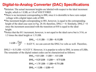
- 17. Digital-to-Analog Converter (DAC) Specifications Differential Nonlinearity : Nonideal components cause the analog increments to differ from their ideal values. The difference between the ideal and nonideal values is known as differential nonlinearity, or DNL and is defined as where n is the number corresponding to the digital input transition. Example 28.4 Determine the DNL for the 3-bit nonideal DAC whose transfer curve is shown in Fig. 28.11. Assume that VREF = 5 V.
- 18. Digital-to-Analog Converter (DAC) Specifications Solution: The actual increment heights are labeled with respect to the ideal increment height, which is 1 LSB, or 1/8 of VOUT/VREF. There is no increment corresponding to 000, since it is desirable to have zero output voltage with a digital input code of 000. The increment height corresponding to 001, however, is equal to the corresponding height of the ideal case seen in Fig. 28.10; therefore, DNL1 = 0. Similarly, DNL2 = 0 since the increment associated with the transition at 010 is equal to the ideal height. Notice that the 011 increment, however, is not equal to the ideal curve but is 3/16, or 1.5 times the ideal height or 1.5 LSB. = 0.625 V, we can convert the DNL3 to volts as well. Therefore, DNL3 = 0.5 LSB = 0.3125 V. However, it is popular to refer to DNL in terms of LSBs. The remainder of the digital output codes can be characterized as follows:
- 19. Digital-to-Analog Converter (DAC) Specifications If we plot the value of DNL (in LSBs) versus the input digital code, Fig. 28.12 would result. The DNL for the entire converter used in this illustration is ±0.75 LSB since the overall error of the DAC is defined by its worst-case DNL. Integral Nonlinearity: Defined as the difference between the data converter output values and a reference straight line drawn through the first and last output values, INL defines the linearity of the overall transfer curve and can be described as
- 20. Digital-to-Analog Converter (DAC) Specifications An illustration of INL measurement is presented in Fig. 28.13. Example 28.5 Determine the INL for the nonideal 3-bit DAC shown in Fig. 28.14. Assume that VREF = 5V.
- 21. Digital-to-Analog Converter (DAC) Specifications Solution: First, a reference line is drawn through the first and last output values. The INL is zero for every code in which the output value lies on the reference line; therefore, INL2 = INL4 = INL6 = INL7 = 0. Only outputs corresponding to 001, 011, and 101, do not lie on the reference. Both the 001 and the 011 transitions occur 1/2 LSB higher than the straight-line values; therefore, INL1 = INL3= 0.5 LSB.
- 22. Digital-to-Analog Converter (DAC) Specifications By the same reasoning, INL5 = -0.75 LSB. Therefore, the INL for the DAC is considered to be its worst-case INL of +0.5 LSB and -0.75 LSB. The INL plot for the nonideal 3-bit DAC can be seen in Fig. 28.15. Offset: The analog output should be 0 V for D = 0. However, an offset exists if the analog output voltage is not equal to zero. This can be seen as a shift in the transfer curve as illustrated in Fig. 28.16. Gain Error: A gain error exists if the slope of the best-fit line through the transfer curve is different from the slope of the best-fit line for the ideal case. For the DAC illustrated in Fig. 28.17, the gain error becomes
- 23. Digital-to-Analog Converter (DAC) Specifications Latency: This specification defines the total time from the moment that the input digital word changes to the time the analog output value has settled to within a specified tolerance. Latency should not be confused with settling time, since latency includes the delay required to map the digital word to an analog value plus the settling time. Signal-to-Noise Ratio (SNR): Signal-to-noise (SNR) is defined as the ratio of the signal power to the noise at the analog output.
- 24. Digital-to-Analog Converter (DAC) Specifications Dynamic Range: Dynamic range is defined as the ratio of the largest output signal over the smallest output signal. For both DACs and ADCs, the dynamic range is related to the resolution of the converter. For example, an N-bit DAC can produce a maximum output of multiples of LSBs and a minimum value of 1 LSB. Therefore, the dynamic range in decibels is simply A 16-bit data converter has a dynamic range of 96.33 dB.
- 25. Analog-to-Digital Converter (ADC) Specifications An ADC accepts an analog signal with an infinite number of values, which then has to be quantized into an N-bit digital word shown in Fig. 28.18 In contrast, the DAC had a finite number of input combinations . The ADC, however, has to "quantize" the infinite-valued analog signal into many segments so that
- 26. Analog-to-Digital Converter (ADC) Specifications
- 27. Analog-to-Digital Converter (ADC) Specifications Examine Fig. 28.19a. The digital output, D, of an ideal, 3-bit ADC is plotted versus the analog input, VIN. Note the difference in the transfer curve for the ADC versus the DAC (Fig. 28.10). The y-axis is now the digital output, and the x-axis has been normalized to VREF, Since the input signal is a continuous signal and the output is discrete, the transfer curve of the ADC resembles that of a staircase. Another fact to observe is that the quantization levels correspond to the digital output codes 0 to 7. Thus, the maximum output of the ADC will be 111 ( ), corresponding to the value for which VIN/VREF > = 7/8. Quantization Error: Since the analog input is an infinite valued quantity and the output is a discrete value, an error will be produced as a result of the quantization. This error, known as quantization error, Qe, is defined as the difference between the actual analog input and the value of the output (staircase) given in voltage. It is calculated as where the value of the staircase output, can be calculated by where D is the value of the digital output code and VLSB is the value of 1 LSB in volts, in
- 28. Analog-to-Digital Converter (ADC) Specifications In Fig. 28.19a, Qe can be generated by subtracting the value of the staircase from the dashed line.The result can be seen in Fig. 28.19b. A sawtooth waveform is formed centered about ½ LSBs. Ideally, the magnitude of Qe will be no greater than one LSB and no less than 0. It would be advantageous if the quantization error were centered about zero so that the error would be at most ±1/2 LSBs (as opposed to +1LSB). This is easily achieved as seen in Fig. 28.20a and b. Here, the entire transfer curve is shifted to the left by 1/2 LSB, thus making the codes centered around the LSB increments on the x-axis. This drawing illustrates that at best, an ideal ADC will have quantization error of ± 1/2 LSB.
- 29. Differential Nonlinearity: Differential nonlinearity for an ADC is similar to that defined for a DAC. However, for the ADC, DNL is the difference between the actual code width of a nonideal converter and the ideal case. Since the step widths can be converted to either volts or LSBs, DNL can be defined using either units. Example 28.6: Using Fig. 28.21a, calculate the differential nonlinearity of the 3-bit ADC. Assume that VREF = 5 V. Draw the quantization error, Qe, in units of LSBs. Analog-to-Digital Converter (ADC) Specifications
- 30. Analog-to-Digital Converter (ADC) Specifications Solution:
- 31. The DNL of the converter can be calculated by examining the step width of each digital output code. Since the ideal step width of the 000 transition is 1/2 LSB, then DNL0 = 0. Also note that the step widths associated with 001 and 100 are equal to 1 LSB; therefore, both DNL2 and DNL4 are zero. However, the remaining values code widths are not equal to the ideal value but can be calculated as The overall DNL for the converter used in this illustration is ±0.5 LSB. Note that the quantization error illustrated in Fig. 28.21b is directly related to the DNL. As DNL increases in either direction, the quantization error worsens. Each "tooth" in the quantization error waveform should ideally be the same size. Missing Codes: Any ADC possessing a DNL that is equal to -1 LSB is guaranteed to have a missing code. Analog-to-Digital Converter (ADC) Specifications
- 32. Analog-to-Digital Converter (ADC) Specifications It is of interest to note the consequences of having a DNL that is equal to -1 LSB. Figure 28.22 illustrates an ADC for which this is true. The total width of the step corresponding to 101 is completely missing; thus, the value of DNL5 is -1 LSB. Notice that the step width corresponding to 010 is 2 LSBs and that the value for DNL2 is +1 LSB. However, there is not a missing code corresponding to 011, since the step width of code 011 depends on the 100 transition. Therefore, an ADC having a DNL greater than +1 LSB is not guaranteed to have a missing code, though in all Example:
- 33. Analog-to-Digital Converter (ADC) Specifications Integral Nonlinearity: Integral nonlinearity (INL) is defined similarly to that for a DAC. Again, a "best-fit“ straight line is drawn through the end points of the first and last code transition, with INL being defined as the difference between the data converter code transition points and the straight line with all other errors set to zero. Example 28.7: Determine the INL for the ADC whose transfer curve is illustrated in Fig. 28.23a. Assume that VREF = 5 V. Draw the quantization error, Qe, in units of LSBs.
- 34. Analog-to-Digital Converter (ADC) Specifications Solution:
- 35. Analog-to-Digital Converter (ADC) Specifications By inspection, it can be seen that all of the transition points occur on the best-fit line except for the transitions associated with code 011 and 110. Therefore, INL0 = INL1 = INL2 = INL4 = INL5 = INL7 =0 The INL corresponding to the remaining codes can be calculated as INL3= 3/8- 5/16 = 1/16 or 0.5 LSB Similarly, INL6 can be calculated in the same manner and is found to be -0.5 LSB. Thus, the overall INL for the converter is the maximum value of INL corresponding to +0.5LSB. The INL can also be determined by inspecting the quantization error in Fig. 28.23b. Here, the INL will be the magnitude of the quantization error which lies outside the ±1/2 LSB band of Qe. It can be seen that Qe = 1 LSB, corresponding to the point at which INL = 0.5 LSB for digital output code 011, and that Qe = -1 LSB at the output code corresponding to INL = -0.5 LSB for digital output code 110. Offset and Gain Error: Offset error: Offset error occurs when there is a difference between the value of the first code transition and the ideal value of 1/2 LSBs. As seen in Fig. 28.24a, the offset error is a constant value. Note that the quantization error becomes ideal after the initial offset voltage is overcome. Gain error: Gain error or scale factor error, seen in Fig. 28.24b, is the difference in the slope of a straight line drawn through the transfer characteristic and the slope of 1 of an ideal ADC.
- 36. Analog-to-Digital Converter (ADC) Specifications
- 37. Analog-to-Digital Converter (ADC) Specifications Aliasing: Nyquist Criterion requires that a signal be sampled at least two times the highest frequency contained in the signal. If this criterion were ignored, a phenomenon known as aliasing would occur. Examine Fig. 28.25. Here, an analog signal is being sampled at a rate slower than the Nyquist Criterion requires. As a result, it appears that a totally different signal (see example dashed line) is being sampled. The different frequency signal is an "alias" of the original signal
- 38. Analog-to-Digital Converter (ADC) Specifications Aliasing can be eliminated by sampling at higher frequencies filtering the analog signal before sampling and removing any frequencies that are greater than one-half the sampling frequency. It is good practice to filter the analog signal before sampling to eliminate any unknown higher order frequency components or noise that could result in aliasing. A frequency domain analysis may further illustrate the concepts of aliasing. Figure 28.26 shows the analog signal, the sampling function (represented by a unit impulse train) and the resulting sampled signal in both the time and frequency domains. The analog signal in Fig. 28.26a is represented as a simple band-limited signal with center frequency, f0. This simply means that the signal is contained within the frequency range shown. In Fig. 28.26b, the sampling function is shown in both the time and frequency domain. The sampling function simply represents the action of sampling at discrete points in time. The frequency domain version of the sampling function is similar to its time domain counterpart, except that the x-axis is now represented as f=1/T. Since each of the impulses has a value of 1, the resulting sampled signal shown in Fig. 28.26c is the impulse function multiplied by the amplitude of the analog signal at each discrete point in time. The multiplication in the time domain is equivalent to convolution in the frequency domain, we note that the frequency domain representation of the sampled signal reveals that the overall signal consists of multiple versions of the band-limited signal at multiples of the sampling frequency.
- 39. Analog-to-Digital Converter (ADC) Specifications Note in Fig. 28.26b that as the sampling time increases, the sampling frequency decreases and the impulses in the frequency domain become more closely spaced. This results in 28.26d, which illustrates the aliasing as the multiple versions of the band-limited signal begin to overlap One could also filter the signal "post-sampling" and eliminate the frequencies for which overlap occurs. The point at which the spectra overlap is called the folding frequency.
- 40. Analog-to-Digital Converter (ADC) Specifications
- 41. Analog-to-Digital Converter (ADC) Specifications Signal-to-Noise Ratio: Signal-to-noise (SNR) ratios of ADCs represent the value of the largest RMS input signal into the converter over the RMS value of the noise. Typically given in dB, the expression for SNR is If it is assumed that the input signal is a sinewave with a peak-to-peak value equal to the full-scale reference voltage VREF of the converter, then the RMS value for vin(max) becomes where VLSB is the voltage value of 1 LSB. The value of the noise will be equivalent to the RMS value of the error signal, Qe . The RMS value of Qe can be calculated to be = Therefore, the SNR for the ideal ADC will be the ratio of these two RMS values,
- 42. Analog-to-Digital Converter (ADC) Specifications which can be written in terms of N as simply
- 43. Thank you