


Digital Design Flow
- 1. By/ Mostafa Khamis mostafaa@riotmicro.com Digital Design Flow
- 2. Digital Design Flow FPGA Vs. ASIC Flow MRAM Controller - Case Study Universal Verification Methodolgy (UVM) About Field Outline
- 4. IC: Integrated Circuits, many transistors on one chip VLSI: Very Large Scale Integration, a modern technology of IC design flow the term vlsi is used to collectively refer to many fields of electrical and computer engineering that deal with the analysis and design of very dense ics a vlsi chip contains more than 106 switching devices or logic gates early in the first decade of the 21st century, the actual number of transistors has exceeded 108 on a silicon die of typically 1 cm2 area= Intoduction
- 5. Design methodology and knowledge change significantly from one component to the other!! System-on-Chip
- 6. Top-Down System Design Flow
- 7. RTL Based Chip Design Flow
- 8. RTL Based Chip Design Flow
- 9. RTL Based Chip Design Flow
- 10. RTL Based Chip Design Flow
- 11. RTL Based Chip Design Flow
- 12. RTL Based Chip Design Flow
- 13. RTL Based Chip Design Flow
- 14. RTL Based Chip Design Flow
- 15. RTL Based Chip Design Flow
- 16. RTL Based Chip Design Flow
- 17. ASIC vs. FPGA Flow
- 19. ASIC design is based on a library of pre-designed and characterized digital cells for a specific fabrication technology. Utilized for smaller production ASICs that are automatically generated by synthesis tools. Library development is a time-consuming and difficult task that must be repeated for every technology generation. From where to get the library: Available from Library vendors/foundries, and qualified at defined foundries. Some ASIC manufacturers (foundries) sell their own library. Layout is often in phantom cells (empty boxes filled at foundry). Build your own library and characterize it: Only large companies. Provide a large library for better synthesis performance. More cells slows down the synthesis tool, which must compare all alternatives. Standard Cell Design Strategy
- 20. Provide a large library of logic cells Deeper stacking and complex functions slows down the circuit, so use simple logic gates AOI32, NAND4, NOR4, XOR2, Majority, ... Storage elements Latch, F/F, embedded logic, reset, scan, ... Multiplexers, Adders, Half-Adders, ... Sophisticated libraries also generate memories of assorted sizes from a graphical user interface. I/O pads. Can be several hundred cells Drive a variety of loads: Usually designers provide different “flavors” of the same gate (binary weighting: x1,x2,x4, x8,x16) Each provide: Symbol, Behavior, Netlist & Layout Standard Cells
- 21. Basic idea: two-dimensional array of logic blocks and flip-flops with a means for the user to configure (program): The function of each block (CLB: Configurable Logic Block). The interconnections between the logic blocks (PSM: Programmable Switch Matrices), Technical viewpoint: For hardware/system-designers, just like ASICs, only better Fabricate a new chip every few hours. Re-configurability In-field Re-programmability At the expense of Performance (speed), Area and Power. Versus ASICs: delay 3-4X, area 40X, and power 12X !! Field-Programmable Gate Arrays- FPGAs
- 22. 4-input look up table (LUT) implements combinational logic functions Register optionally stores output of LUT Idealized CLB
- 23. MRAM Controller – Case Study
- 24. MRAM Specs Doc
- 25. MRAM Controller Architecture Level
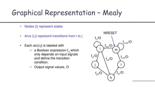
- 27. Graphical Representation – Mealy
- 28. Graphical Representation – Moore
- 32. What? SystemVerilog is a language just like Verilog and has its own constructs, syntax and features, but UVM is a framework of SystemVerilog classes from which fully functional testbenches can be built. There's only one prerequisite to learn UVM, and that is SystemVerilog because it is the foundation for the tower that is UVM. Why? The primary advantage is that the methodology specifies and lays out a set of guidelines to be followed for creation of verification testbenches. This will ensure testbench uniformity between different verification teams, cross-compatability between IP and standalone environment integration, flexibility and ease of maintaining testbenches. Universal Verification Methodology (UVM)
- 33. Every verification testbench has a few key components like drivers, monitors, stimulus generators, and scoreboards. UVM provides a base class for each of these components with standardized functions to instantiate, connect and build the testbench environment. These are static entities called componentsin a verification environment that exist throughout a simulation just like buildings in a city. These components operate and process on some kind of data that flows around the environment similar to people and vehicles in the city. The data or transactions are called objects or sequence items since they appear and disappear at various times in the simulation and is more dynamic in nature. How does UVM help ?
- 35. About Field