![The Cell Broadband Engine: Exploiting multiple levels of
parallelism in a chip multiprocessor
Michael Gschwind
IBM T.J. Watson Research Center
Yorktown Heights, NY
Abstract
As CMOS feature sizes continue to shrink and traditional microarchitectural methods for delivering high per-
formance (e.g., deep pipelining) become too expensive and power-hungry, chip multiprocessors (CMPs) become an
exciting new direction by which system designers can deliver increased performance. Exploiting parallelism in such
designs is the key to high performance, and we find that parallelism must be exploited at multiple levels of the sys-
tem: the thread-level parallelism that has become popular in many designs fails to exploit all the levels of available
parallelism in many workloads for CMP systems.
We describe the Cell Broadband Engine and the multiple levels at which its architecture exploits parallelism:
data-level, instruction-level, thread-level, memory-level, and compute-transfer parallelism. By taking advantage of
opportunities at all levels of the system, this CMP revolutionizes parallel architectures to deliver previously unattained
levels of single chip performance.
We describe how the heterogeneous cores allow to achieve this performance by parallelizing and offloading
computation intensive application code onto the Synergistic Processor Element (SPE) cores using a heterogeneous
thread model with SPEs. We also give an example of scheduling code to be memory latency tolerant using software
pipelining techniques in the SPE.
1 Introduction
As chip multiprocessors (CMPs) become the new direction for future systems in the industry, they are also spurring
a new burst of computer architecture innovation. This increase in new innovative solutions is a result of new con-
straints which require new techniques to overcome the technology’s limitations in ways previous generations’ tech-
niques could not. A confluence of factors is leading to a surge in CMP designs across the industry. From a purely
performance-centric view, frequency scaling is running out of steam: technology-based frequency improvements are
increasingly difficult, while the performance potential of deeper pipelining is all but exhausted.
While chip multiprocessors have been touted as an approach to deliver increased performance, adoption had been
slow because frequency scaling had continued to deliver performance improvements for uniprocessor designs until
recently. However, at the turn of the millennium, the diminishing returns of uniprocessor designs became painfully
clear, and designers started to turn to chip multiprocessing to deliver a significant performance boost over traditional
uniprocessor-centric solutions.
In addition to addressing performance limitations of uniprocessor designs, CMPs also offer a way to address power
dissipation which has become a first class design constraint. While deep pipelining offers only small performance
gains for an incommensurate increase in power dissipation and makes deeply pipelined designs unattractive under
power dissipation constraints [21], exploiting higher-level application parallelism delivers performance increases for
smaller marginal power increases.
The emergence of chip multiprocessors is the effect of a number of shifts taking place in the industry: limited
returns on deep pipelining, reduced benefits of technology scaling for higher frequency operation, and a power crisis
making many “traditional” solutions non-viable. Another challenge that architects of high performance systems must
address is the burgeoning design and verification complexity and cost, while continuing to find ways to translate the
increased density of new CMOS technologies, based on Dennard’s scaling theory [8], into delivered performance.
1](https://image.slidesharecdn.com/exploitingmultiplelevelsofparallelism-210125023903/85/Michael-Gschwind-Cell-Broadband-Engine-Exploiting-multiple-levels-of-parallelism-in-a-Chip-Multiprocessor-2-320.jpg)
![The situation in many ways mirrors the dawn of RISC architectures, and it may be useful to draw the parallels.
Then, as now, technological change was rife. The emerging large scale integration production enabled the building
of competitive processors using a single chip, with massive cost reductions. Alas, the new technology presented
constraints in the form of device count, limiting design complexity and making streamlined new architectures –
microprocessors – a preferred class.
At the same time, pipelined designs showed a significant performance benefit. With the limited CAD tools avail-
able for design and verification at the time, this gave a significant practical advantage to simpler designs that were
tractable with the available tools. Finally, the emergence of new compiler technologies helping to marshal the perfor-
mance potential using instruction scheduling to exploit pipelined designs and performing register allocation to handle
the increasingly severe disparity between memory and processor performance rounded out the picture.
Then, as now, innovation in the industry was reaching new heights. Where RISC marked the beginning of single
chip processors, chip multiprocessors mark the beginning of single chip systems. This increase in new innovative
solutions is a response to new constraints invalidating the established solutions, giving new technologies an oppor-
tunity to overcome the incumbent technology’s advantages. When the ground rules change, high optimization often
means that established technologies cannot respond to new challenges. Innovation starts slowly, but captures pub-
lic perception in a short, sudden instant when the technology limitations become overbearing [5]. Thus, while chip
multiprocessors have conceptually been discussed for over a decade, they have now become the most promising and
widely adopted solution to deliver increasing system performance across a wide range of applications.
We discuss several new concepts introduced with the Cell Broadband Engine (Cell BE), such as heterogeneous
chip multiprocessing using accelerator cores. The accelerator cores offer a new degree of parallelism by supporting
independent compute and transfer threads within each accelerator core. The SPE cores are fully integrated into the
system architecture and share the virtual memory architecture, exception architecture, and other key system features
with the Power Architecture core which serves as the foundation of the Cell Broadband Engine Architecture. The
accelerator cores can be programmed using a variety of programming models ranging from a traditional function
accelerator based on an RPC model to functional processing pipelines of several accelerator cores.
We also describe new programming models for heterogeneous cores based on a heterogeneous threading model
which allows SPE threads to execute autonomously within a process space. SPE threads can independently fetch
their data from system memory by issuing DMA transfer commands. By applying compiler-based latency tolerating
techniques such as software pipelining to memory latencies, and by exploiting the parallelism between decoupled
execution and system memory access, applications can be accelerated beyond the exploitation of the parallelism
provided between the SPE cores.
This paper is structured as follows: In section 2, we give an overview the architecture of the Cell BE. We describe
how the Cell BE exploits application parallelism in section 3, and describe how the system memory architecture of the
Cell BE facilitates the exploitation of memory-level parallelism. We describe the Cell SPE memory flow controller
in detail in section 5. Section 6 describes programming models for the Cell BE, and describes program initialization
for integerated execution in the Cell BE. Section 7 describes SPE programming and the heterogeneous multithreaded
programming model. We discuss system architecture issues for chip multiprocessors in section 8 and close with an
outlook in section 9.
2 The Cell Broadband Engine
The Cell Broadband Engine (Cell BE) was designed from ground up to address the diminishing returns available from
a frequency-oriented single core design point by exploiting application parallelism and embracing chip multiprocess-
ing.
As shown in figure 1, we chose a heterogeneous chip multiprocessing architecture consisting of two different
core types in order to maximize the delivered system performance [16, 15]. In the Cell BE design, Power Proces-
sor Elements (PPEs) based on the IBM Power Architecture deliver system-wide services, such as virtual memory
management, handling exceptions, thread scheduling and other operating system services.
The Synergistic Processor Elements (SPEs) deliver the majority of a Cell BE system’s compute performance.
SPEs are accelerator cores implementing a novel, pervasively data-parallel computing architecture based on SIMD
RISC computing and explicit data transfer management.
An SPE consists of two components, the Synergistic Processing Unit (SPU) and the Synergistic Memory Flow
Controller (MFC), which together provide each SPE thread with the capability to execute independent compute and
2](https://image.slidesharecdn.com/exploitingmultiplelevelsofparallelism-210125023903/85/Michael-Gschwind-Cell-Broadband-Engine-Exploiting-multiple-levels-of-parallelism-in-a-Chip-Multiprocessor-3-320.jpg)

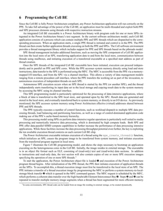
![MFC
VRF
PERM LSU
V F P U
V F P U V F X U
Local Store
Single Port
SRAM
Issue /
Branch
Fetch
ILB
16B x 2
2 instructions
16B x 3 x 2
64B
16B
128B
Figure 2: The Synergistic Processor Unit fetches instructions using a statically scheduled frontend which can issue
a bundle with up to two instructions per cycle to the data-parallel backend. The backend shares execution units for
scalar and SIMD processing by layering scalar computation on data-parallel execution paths. This reduces area and
power dissipation by reducing the number of issue ports, simplifying dependence checking and bypassing logic and
reducing the number of execution units per core.
Atomic Facility The atomic facility provides a snoop-coherentcache to implement load-and-reserve/store-conditional
memory synchronization, and for use during hardware page table walks by the MMU. The MFC provides load-
and-reserve and store-conditional commands that can be used to synchronize data between the SPEs, or between
SPEs and PPEs executing the Power Architecture load-and-reserve and store conditional instructions.
Bus Interface Control The bus interface provides the memory flow controller with access to the high-speed on-chip
element interconnect bus (EIB), and access to memory mapped registers which provide an interface to issue
DMA requests from remote processor elements, to update the virtual memory translations and to configure the
MFC.
The Cell Broadband Engine Architecture specifies a heterogeneous architecture with two distinct core types and
integrates them into a system with consistent data types, consistent operation semantics, and a consistent view of
the virtual memory system. As a result, the Cell BE transcends prior systems consisting of collections of different
processors, but rather represents a novel system architecture based on the integration of core types optimized for
specific functions.
Gschwind et al. [13, 14] gives an overview of the Cell Synergistic Processor architecture based on a pervasively
data parallel computing (PDPC) approach, and Flachs et al. [10] describes the SPE microarchitecture.
3 Exploiting Application Parallelism
To deliver a significant increase in application performance in a power-constrained environment, the Cell BE design
exploits application parallelism at all levels:
data level parallelism with pervasive SIMD instruction support,
instruction-level parallelism using a statically scheduled and power aware microarchitecture,
compute-transfer parallelism using programmable data transfer engines,
thread-level parallelism with a multi-core design approach, and hardware multithreading on the PPE, and
memory-level parallelism by overlapping transfers from multiple requests per core and from multiple cores.
To provide an architecture that can be exploited efficiently by applications, it is important to provide the right
amount of parallelism at each level. Delivering more parallel resources at any of the parallelism levels than can be
4](https://image.slidesharecdn.com/exploitingmultiplelevelsofparallelism-210125023903/85/Michael-Gschwind-Cell-Broadband-Engine-Exploiting-multiple-levels-of-parallelism-in-a-Chip-Multiprocessor-5-320.jpg)

![datapaths.
Sharing of execution units for scalar and SIMD processing can be accomplished either architecturally, as in the Cell
SPE which has a single architectural register file to store scalar and SIMD data (see figure 2), or microarchitecturally
for floating point and media computations, as in the Cell PPE which implements both types of computations in the
same processing unit. In addition to resource efficiency, architectural sharing further increases efficiency of SIMD
software exploitation by reducing data sharing cost.
The Cell BE design also exploits instruction level parallelism with a statically scheduled power-aware multi-issue
microarchitecture. We provide statically scheduled parallelism between execution units to allow dual instruction
issue for both the PPE and SPE cores. On both cores, dual issue is limited to instruction sequences that match
the provisioned execution units of a comparable single-issue microprocessor. This is limiting in two respects: (1)
instructions must be scheduled to match the resource profile as no instruction re-ordering is provided to increase the
potential for multi-issue; and (2) execution units are not duplicated to increase multi-issue potential.
While these decisions represent a limitation on dual issue, they imply that parallel execution is inherently power-
aware. No additional reorder buffers, register rename units, commit buffers or similar structures are necessary, reduc-
ing core power dissipation. Because the resource profile is known, a compiler can statically schedule instructions to
the resource profile.
Instruction-level parallelism as used in the Cell Broadband Engine avoids the power inefficiency of wide issue
architectures, because no execution units with their inherent static and dynamic power dissipation are added for
marginal performance increase.
Instead, parallel execution becomes energy-efficient because the efficiency of the core is increased by dual issuing
instructions: instead of incurring static power for an idle unit, the execution is performed in parallel, leading directly
to a desirable reduction in energy-delay product.
To illustrate, as a first order approximation, let us consider energy to consist of the sum of energy per operation
to execute all operations of a program ecompute and a leakage power component dissipated over the entire execution
time of the program eleakage. For normalized execution time t = 1, this gives a normalized energy delay metric of
(ecompute + eleakage).
By speeding up execution time using parallel execution, but without adding hardware mechanisms or increasing
the level of speculation, the energy-delay product is reduced. The new reduced execution time s, s < 1, is a frac-
tion of the original (normalized) execution time t. The energy-delay product of power-aware parallel execution is
(ecompute + eleakage × s) × s. Note that both the energy and delay factors of the energy-delay product are reduced
compared to non-parallel execution. The total energy is reduced by scaling the leakage power to reflect the reduced
execution time, whereas the energy ecompute remains constant, as the total number of executed operations remains
unchanged.
In addition to speeding execution time by enabling parallel computation, ILP also can improve average memory
latency by concurrently servicing multiple outstanding cache misses. In this use of ILP, a processor continues exe-
cution across a cache miss to encounter clusters of cache misses. This allows the concurrent initiation of the cache
reload for several accesses and the overlapping of a sequence of memory accesses. The Cell BE cores support a
stall-on-use policy which allows applications to initiate multiple data cache reload operations. Large register sets and
simple deterministic scheduling rules facilitate scheduling overlapped memory accesses ahead of data use.
While ILP provides a good vehicle to discover cache misses that can be serviced in parallel, it only has limited
success in overlapping computation with the actual data cache miss service. Intuitively, instruction level parallelism
can only cover a limited amount of the total cache miss service delay, a result confirmed by Karkhanis and Smith [17].
Thread-level parallelism (TLP) is supported with a multi-threaded PPE core and multiple SPE cores on a single
Cell Broadband Engine chip. TLP delivers a significant boost in performance by providing ten independent execution
contexts to multithreaded applications, with a total performance exceeding 200 GFLOPS. TLP is a key to delivering
high performance with high power/performance efficiency, as described by Salapura et al. [19, 20].
To ensure performance of a single thread, we also exploit a new form a parallelism that we refer to as compute-
transfer parallelism (CTP). To exploit available memory bandwidth more efficiently, and to decouple and parallelize
data transfer and processing, compute-transfer parallelism considers data movement as an explicitly scheduled oper-
ation that can be controlled by the program to improve data delivery efficiency. Using application-level knowledge,
explicit data transfer operations are inserted into the instruction stream sufficiently ahead of their use to ensure data
availability and to reduce program idle time. Unlike software-directed data prefetch, which offers access to small
amounts of data per prefetch request, compute-transfer parallelism is independently sequenced and targets block
6](https://image.slidesharecdn.com/exploitingmultiplelevelsofparallelism-210125023903/85/Michael-Gschwind-Cell-Broadband-Engine-Exploiting-multiple-levels-of-parallelism-in-a-Chip-Multiprocessor-7-320.jpg)
![computation mem protocol
mem protocol mem idle
mem idle mem contention
mem contention
computation
parallel
memory accesses
memory interface
computation
memory accesses
memory interface
(a)
(b)
time
Figure 4: Cache miss scenarios for single threaded workloads: (a) Isolated cache misses incur the full latency per
access, with limited compute/memory overlap during the initial memory access phase. (b) By discovering clusters of
cache misses and overlapping multiple outstanding cache misses, the average memory latency is reduced by a factor
corresponding to the application memory level parallelism (MLP).
transfers of up to 16KB per request and transfer list commands. In the Cell Broadband Engine, bulk data transfers are
performed by eight Synergistic Memory Flow Controllers coupled to the eight Synergistic Processor Units.
Finally, to deliver a balanced CMP system, addressing the memory bottleneck is of prime importance to sustain
application performance. Today, memory performance is already limiting performance of a single thread. Increasing
per-thread performance becomes possible only by addressing the memory wall head-on [23]. To deliver a balanced
system design with a chip multiprocessor, the memory interface utilization must be improved even more because
memory interface bandwidth is growing more slowly than aggregate chip computational performance.
4 A System Memory Architecture for Exploiting MLP
Chip multiprocessing offers an attractive way to implement TLP processing in a power-efficient manner. However,
to translate peak MIPS and FLOPS of a chip multiprocessor into sustained application performance, efficient use
of memory bandwidth is key. Several design points promise to address memory performance with the parallelism
afforded by chip multiprocessing.
The key to exploiting memory bandwidth is to achieve high memory-level parallelism (MLP), i.e., to increase the
number of simultaneously outstanding cache misses. This reduces both the average service time, and increases overall
bandwidth utilization by interleaving of multiple memory transactions [11].
Figure 4 shows two typical execution scenarios for a single thread, with varying memory-level parallelism, corre-
sponding to two isolated cache misses and two concurrently serviced cache misses. While isolated cache misses incur
the full latency per access, with limited compute/memory overlap during the initial memory access phase, overlapping
cache misses can significantly reduce the average memory service time per transaction.
In this and the following diagrams, time flows from left to right. We indicate execution progress in the core with
the computation and memory access transaction bars. In addition, we show utilization of the memory interface based
on the memory transactions in flight. Memory accesses are broken down into actual protocol actions for protocol
requests and replies including data transfers (“mem protocol”), idle time when the bus is unused by a transaction
(“mem idle”), and queuing delays for individual transactions due to contention (“mem contention”).
The first scenario (a) depicts serial miss detection, such as might be typical of pointer chasing code. An access
missing in the cache causes an access to a next memory hierarchy level. With the common stall-on-use policy,
execution and memory access can proceed in parallel until a dependence is encountered, giving a limited amount of
compute and transfer parallelism. The key problem with these types of sequences is that isolated memory accesses are
followed by short computation sequences, until the next cache line must be fetched, and so forth. This is particularly
7](https://image.slidesharecdn.com/exploitingmultiplelevelsofparallelism-210125023903/85/Michael-Gschwind-Cell-Broadband-Engine-Exploiting-multiple-levels-of-parallelism-in-a-Chip-Multiprocessor-8-320.jpg)
![computation mem protocol
mem protocol mem idle
mem idle mem contention
mem contention
computation
memory accesses
computation
memory accesses
computation
memory accesses
computation
memory accesses
memory interface
thread 1:
thread 2:
thread 3:
thread 3:
time
Figure 5: When multiple thread contexts are operating on a chip, memory requests from several threads can be
interleaved. This improves utilization of the memory bandwidth across the off-chip interface by exploiting memory-
level parallelism between threads. However, cross-thread MLP does not improve an individual thread’s performance.
problematic for “streaming” computations (i.e., those exhibiting low temporal locality, whether truly streaming, or
with large enough working sets to virtually guarantee that no temporal locality can be detected).
The second scenario (b) adds parallelism between multiple outstanding accesses. This code may be found when
instruction scheduling is performed to initiate multiple memory accesses, such as for compute-intensive applications
using tiling in register files and caches. Stall-on-use policy is important to allow discovery of multiple cache misses
and initiation of multiple concurrent memory requests as long as no data dependences exist. This parallelism is also
referred to as MLP, and reduces overall program execution time by overlapping multiple long latency operations [11].
The actual memory interface utilization in both instances is rather low, pointing to inefficient use of the memory
interface.
By implementing chip architectures that provide multiple threads of execution on a chip, non-stalled threads can
continue to compute and discover independent memory accesses which need to be serviced. This improves utilization
of an important limited resource, off-chip bandwidth. This was a concept popularized by the Cyclops architecture
[22, 3] and found its way into other systems, such as Niagara.
The Cyclops approach exploits a high-bandwidth on-chip eDRAM solution. Although this alleviates the memory
latency problem, access to data still takes multiple machine cycles. The Cyclops solution is to populate the chip with
a large number of thread units. Each thread unit behaves like a simple, single-issue, in-order processor. Expensive
resources, like floating-point units and caches, are shared by groups of threads to ensure high utilization. The thread
units are independent. If a thread stalls on a memory reference or on the result of an operation, other threads can
continue to make progress. The performance of each individual thread is not particularly high, but the aggregate chip
performance is much better than a conventional single-threaded uniprocessor design with an equivalent number of
transistors. Large, scalable systems can be built with a cellular approach using the Cyclops chip as a building block
[22, 3]. A similar approach to increase off-chip memory bandwidth utilization was later described by [4] and is used
in Sun’s Niagara system.
Figure 5 shows how a threaded environment can increase memory level parallelism between threads (this can
combine with MLP within a thread, not shown). Thread-based MLP uses several threads to discover misses for each
thread, to improve memory utilization, but still accepts that threads will be stalled for significant portions of the time.
This model corresponds to execution on heavily threaded CMPs (Piranha [2], Cyclops, Niagara). Multi-threading
within a core can then be used to better utilize execution units either by sharing expensive execution units, or by using
multiple threads within a core.
Figure 6 shows compute-transfer and memory parallelism as provided by the Cell Broadband Engine Architecture.
As described in section 2, each SPE consists of separate and independent subunits, the SPU directed at data processing,
and the MFC for bulk data transfer between the system memory and an SPU’s local store. This architecture gives
programmers new ways to achieve application performance by exploiting compute-transfer parallelism available in
8](https://image.slidesharecdn.com/exploitingmultiplelevelsofparallelism-210125023903/85/Michael-Gschwind-Cell-Broadband-Engine-Exploiting-multiple-levels-of-parallelism-in-a-Chip-Multiprocessor-9-320.jpg)

![and their variable latency, compilers typically must ignore cache behavior during the instruction scheduling phase and
assume optimistic hit timings for all accesses.
In comparison, the local store abstraction provides a dense, single-ported operand data storage with determin-
istic access latency, and provides the ability to perform software-managed data replacement for workloads with
predictable data access patterns. This allows exploitation of compiler-based latency tolerating techniques, such as
software pipelining being applied to efficiently hide long latency memory operations.
5 Optimizing Performance with the Synergistic Memory Flow Controller
The Cell BE implements a heterogeneous chip multiprocessor consisting of the PPE and SPEs, with the first imple-
mentation integrating one PPE and eight SPEs on a chip. The PPE implements a traditional memory hierarchy based
on a 32KB first level cache and a 512 KB second level cache.
The SPEs use the Synergistic Memory Flow Controller (MFC) to implement memory access. The Memory Flow
Controller provides the SPE with the full Power Architecture virtual memory architecture, using a two-level translation
hierarchy with segment and page tables. A first translation step based on the segment tables maps effective addresses
used by application threads to virtual addresses, which are then translated to real addresses using the page tables.
Compared with traditional memory hierarchies, the Synergistic Memory Flow Controller helps reduce the cost of
coherence and allows applications to manage memory access more efficiently.
Support for the Power Architecture virtual memory translation gives application threads full access to system
memory, ensuring efficient data sharing between threads executing on PPEs and SPEs by providing a common view
of the address space across different core types. Thus, a Power Architecture effective address serves as the common
reference for an application to reference system memory, and can be passed freely between PPEs and SPEs.
In the PPE, effective addresses are used to specify memory addresses for load and store instructions of the Power
Architecture ISA. On the SPE, these same effective addresses are used by the SPE to initiate the transfer of data be-
tween system memory and the local store by programming the Synergistic Memory Flow Controller. The Synergistic
Memory Flow Controller translates the effective address, using segment tables and page tables, to an absolute address
when initiating a DMA transfer between an SPE’s local store and system memory.
In addition to providing efficient data sharing between PPE and SPE threads, the Memory Flow Controller also
provides support for data protection and demand paging. Since each thread can reference memory only in its own
process’s memory space, memory address translation of DMA request addresses provides protection between multiple
concurrent processes. In addition, indirection through the page translation hierarchy allows pages to be paged out.
Like all exceptions generated within an SPE, page translation-related exceptions are forwarded to a PPE while the
memory access is suspended. This allows the operating system executing on the PPE to page in data as necessary and
restart the MFC data transfer when the data has been paged in.
MFC data transfers provide coherent data operations to ensure seamless data sharing between PPEs and SPEs.
Thus, while performing a system memory to local store transfer, if the most recent data is contained in a PPE’s cache
hierarchy, the MFC data transfer will snoop the data from the cache. Likewise, during local store to system memory
transfers, cache lines corresponding to the transferred data region are invalidated to ensure the next data access by
the PPE will retrieve the correct data. Finally, the Memory Flow Controller’s memory management unit maintains
coherent TLBs with respect to the system-wide page tables [1].
While the memory flow controller provides coherent transfers and memory mapping, a data transfer from system
memory to local store creates a data copy. If synchronization between multiple data copies is required, this must be
provided by an application-level mechanism.
MFC transfers between system memory and an SPE’s local store can be initiated either by the local SPE using
SPU channels commands, or by remote processor elements (either a PPE or an SPE) by programming the MFC via its
memory mapped I/O interface. Using self-paced SPU accesses to transfer data is preferable to remote programming
because transfers are easier to synchronize with processing from the SPE by querying the status channel, and because
SPU channel commands offer better performance. In addition to the shorter latency involved in issuing a channel
instruction from the SPU compared to a memory mapped I/O access to an uncached memory region, the DMA request
queue accepting requests from the local SPU contains 16 entries compared to the eight entries available for buffering
requests from remote nodes. Some features, such as the DMA list command, are only available from the local SPE
via the channel interface.
10](https://image.slidesharecdn.com/exploitingmultiplelevelsofparallelism-210125023903/85/Michael-Gschwind-Cell-Broadband-Engine-Exploiting-multiple-levels-of-parallelism-in-a-Chip-Multiprocessor-11-320.jpg)

![tion over a data array executing on the PPE:
ppe_sum_all(float *a)
{
for (i=0; i<MAX; i++)
sum += a[i];
}
The same function can be expressed to be performed on the SPE (and operating on multiple SPEs in parallel to
achieve greater aggregate throughput):
spe_sum_all(float *a)
{
/* Declare local buffer */
static float local_a[MAX] __attribute__ ((aligned (128)));
/* initiate an MFC transfer from system memory to local buffer
system memory address: a[0]
local memory address: local_a[0]
transfer size: elements * element size bytes
tag: 31
*/
mfc_get(&local_a[0], &a[0], sizeof(float)*MAX, 31, 0, 0);
/* define tag mask for subsequent MFC commands */
mfc_write_tag_mask(1<<31);
/* wait for completion of request with specified tag 31 */
mfc_read_tag_status_all();
/* perform algorithm on data copy in local store */
for (i=0; i<MAX; i++)
sum += local_a[i];
}
Notice that in this example, the SPE function receives the same effective address for the array a, which is then used
to initiate a DMA transfer, and the SPE performs all further data pacing autonomously without interaction from other
processor elements (other than paging service performed by the operating system executing on the PPE in response to
page faults which may be triggered by DMA requests).
The address of the initial request can be obtained using variety of communication channels available between
processing elements. These include embedding the address in the SPE executable (either at compile time for static
data, or at thread creation time by patching the executable to insert a dynamic address at a defined location in the
executable) using a direct Power Architecture store instruction from the PPE into the local store which can be mapped
into the system memory address space, using the mailbox communication channel, or using a memory flow controller
transfer to local store initiated from a remote processor element.
Once a first address is available in the SPE thread, the SPE thread can generate derivative addresses by indexing or
offsetting this address, or by using pointer indirection from effective address pointers transferred to local store using
memory flow controller transfers.
To achieve maximum performance, this programming model is best combined with data double buffering (or even
triple buffering), using a software-pipelining model for MFC-based data transfers where a portion of the working set is
being transferred in parallel to execution on another portion. This approach leverages the compute-transfer parallelism
inherent in each SPE with its independent SPU execution and MFC data transfer threads [12].
spe_sum_all(float *a)
{
13](https://image.slidesharecdn.com/exploitingmultiplelevelsofparallelism-210125023903/85/Michael-Gschwind-Cell-Broadband-Engine-Exploiting-multiple-levels-of-parallelism-in-a-Chip-Multiprocessor-14-320.jpg)
![/* Declare local buffer */
static float local_a[CHUNK*2] __attribute__ ((aligned (128)));
unsigned int j, xfer_j, work_j;
/*************************************************************/
/* prolog: initiate first iteration */
/* initiate an MFC transfer from system memory to local buffer
system memory address: a[0]
local memory address: local_a[0]
transfer size: elements * element size bytes
tag: 30
*/
mfc_get(&local_a[0], &a[0], sizeof(float)*MAX, 30, 0, 0);
/*************************************************************/
/* steady state: operate on iteration j-1, fetch iteration j */
for (j = 1 ; j < MAX/CHUNK; j++)
{
xfer_j = j%2;
work_j = (j-1)%2;
/* initiate an MFC transfer from system memory to
local buffer for the next iteration (xfer_j)
system memory address: a[0+offset]
local memory address: local_a[]
transfer size: elements * element size bytes
tag: xfer_j
*/
mfc_get(&local_a[xfer_j*CHUNK], &a[j*CHUNK], sizeof(float)*MAX, 30+xfer_j, 0, 0);
/* define tag mask for subsequent MFC commands to point to
transfer (work_j) */
mfc_write_tag_mask(1<<(30+work_j));
/* wait for completion of request with tag for current iteration */
mfc_read_tag_status_all();
/* perform algorithm on data copy for (work_j) in local store */
for (i=0; i<CHUNK; i++)
sum += local_a[work_j*CHUNK+i];
}
/*************************************************************/
/* epilog: perform algorithm on last iteration */
work_j = (j-1)%2;
/* define tag mask for subsequent MFC commands to point to
previous transfer */
14](https://image.slidesharecdn.com/exploitingmultiplelevelsofparallelism-210125023903/85/Michael-Gschwind-Cell-Broadband-Engine-Exploiting-multiple-levels-of-parallelism-in-a-Chip-Multiprocessor-15-320.jpg)
![Figure 8: Cell Broadband Engine implementation: The first implementation of the Cell Broadband Engine Architec-
ture integrates an I/O controller, a memory controller and multiple high-speed interfaces with the Cell heterogeneous
chip multiprocessor connected by the high-speed element interconnect bus. Providing system functions in the Power
Architecture core as a shared function and an architectural emphasis on data processing in the SPEs delivers unprece-
dented compute performance in a small area.
mfc_write_tag_mask(1<<(30+work_j));
/* wait for completion of request with tag for current iteration */
mfc_read_tag_status_all();
for (i=0; i<CHUNK; i++)
sum += local_a[work_j*CHUNK+i];
}
8 System Architecture
While the discussion of CMPs often exhausts itself with the discussion of the “right core” and “the right number
of cores”, CMPs require a range of system design decisions to be made. Integration of system functionality is an
important aspect of CMP efficiency, as increasing the number of cores on a die limits the signal pins available to each
core. Thus, as seen in figure 8 functionality previously found in system chipsets, such as coherence management,
interrupt controllers, DMA engines, high-performance I/O and memory controllers are increasingly integrated on the
die.
While discussions about chip multiprocessing often concern themselves only with discussing the number, homoge-
neous or heterogeneous make-up, and feature set of cores for chip multiprocessors, a chip multiprocessor architecture
describes a system architecture, not just a microprocessor core architecture.
Corresponding to the scope of CMP systems which can be built from Cell BE chips, the Cell BE is a system
architecture, which integrates a number of functions that previously have been provided as discrete elements on the
system board, including the coherence logic between multiple processor cores, the internal interrupt controller, two
configurable high-speed I/O interfaces, a high-speed memory interface, a token manager for handling bandwidth
reservation, and I/O translation capabilities providing address translation for device-initiated DMA transfers.
Providing individual off-chip interfaces for each core as described by McNair et al. [18] leads to increased
bandwidth requirements, longer latencies and is inherently unscalable with respect to the number of cores that can be
supported.
Integration of system functionality offers several advantages. From a performance perspective, integrating system
function eliminates design constraints imposed by off-chip latency and bandwidth limitations. From a cost perspective,
15](https://image.slidesharecdn.com/exploitingmultiplelevelsofparallelism-210125023903/85/Michael-Gschwind-Cell-Broadband-Engine-Exploiting-multiple-levels-of-parallelism-in-a-Chip-Multiprocessor-16-320.jpg)
![Cell BE
Processor
XDR™ XDR™
IOIF0 IOIF1
(a) Single node configuration with dual I/O inter-
faces
Cell BE
Processor
XDR™ XDR™
IOIF BIF
Cell BE
Processor
XDR™ XDR™
IOIF
(b) Dual node glueless configuration with one
I/O interface per node, and a port configured
as Broadband Engine Interface connecting two
nodes
Cell BE
Processor
XDR™ XDR™
IOIF
BIF
Cell BE
Processor
XDR™ XDR™
IOIF
Cell
BE
Processor
XDR
™ XDR
™
IOIF
BIF
Cell
BE
Processor
XDR
™ XDR
™
IOIF
switch
(c) Multi-node configurations interconnect multi-
ple nodes using a switch attached to ports config-
ured as Broadband Engine Interface
Figure 9: The Cell Broadband Engine implementation supports multiple configurations with a single part, ranging
from single node systems to multi-node configurations.
reducing the number of necessary parts offers a more cost-effective way to build systems. However, integration
can also limit the number of system configurations that can be supported with a single part, and may reduce the
flexibility for specifying and differentiating a specific system based on the chipset capabilities. Thus, a scalable
system architecture that supports a range of configuration options will be an important attribute for future CMPs.
In the Cell BE architecture, configurability and a wide range of system design options are provided by ensuring
flexibility and configurability of the system components. As an example of such scalability, the Cell Broadband Engine
contains several high-speed interfaces. As shown in figure 9, two high-performance interfaces may be configured as
I/O interfaces in a single node configuration to provide I/O capacity in personal systems for a high-bandwidth I/O
device (e.g., a frame buffer). Alternatively, one I/O interface can be reconfigured to serve as a Broadband Engine
Interface to configure a glueless dual node system to extend the Element Interconnect Bus across two Cell BE chips,
providing a cost-effective entry-level server configuration with two PPE and 16 SPE processor elements. Larger server
configurations are possible by using a switch to interconnect multiple Cell Broadband Engine chips [6].
16](https://image.slidesharecdn.com/exploitingmultiplelevelsofparallelism-210125023903/85/Michael-Gschwind-Cell-Broadband-Engine-Exploiting-multiple-levels-of-parallelism-in-a-Chip-Multiprocessor-17-320.jpg)
![9 Outlook
The number of chip multiprocessors announced has burgeoned since the introduction of the first Power4 systems.
In the process, a range of new innovative solutions has been proposed and implemented, from CMPs based on ho-
mogeneous single ISA systems (Piranha, Cyclops, Xbox360), to heterogenous multi-ISA systems (such as the Cell
Broadband Engine). In addition to stand-alone systems, application-specific accelerator CMPs are finding a niche to
accelerate specific system tasks, e.g., the Azul 384-way Java appliance [7].
Finally, architecture innovation in chip multiprocessors is creating a need for new, innovative compilation tech-
niques to harness the power of the new architectures by parallelizing code across several forms of parallelism, ranging
from data-level SIMD parallelism to generating a multi-threaded application from a single threaded source program
[9]. Other optimizations becoming increasingly important include data privatization, local storage optimizations and
explicit data management, as well as transformations to uncover and exploit compute-transfer parallelism.
Today’s solutions are a first step towards exploring the power of chip multiprocessors. Like the RISC revolution,
which ultimately led to the high-end uniprocessors ubiquitous today, the CMP revolution will take years to play out in
the market place. Yet, the RISC revolution also provides a cautionary tale – as technology became more mature, the
first mover advantage and peak performance became less important than customer value. Today, both high end and
low end systems are dominated by CISC architectures based on RISC microarchitectures ranging from commodity
AMD64 processors to high-end System z servers that power the backbone of reliable and mission critical systems.
Chip multiprocessing provides a broad technology base which can be used to enable new system architectures with
attractive system tradeoffs and better performance than existing system architectures. This aspect of chip multipro-
cessors has already led to the creation of several novel exciting architectures, such as the Azul Java appliance and Cell
Broadband Engine. At the same time, chip multiprocessing also provides a technology base to implement compatible
evolutionary systems. The Cell Broadband Engine bridges the divide between revolutionary and evolutionary design
points by leveraging the scalable Power ArchitectureTM
as the foundation of a novel system architecture, offering both
compatibility and breakthrough performance.
10 Acknowledgments
The author wishes to thank Peter Hofstee, Ted Maeurer and Barry Minor for many insightful discussions. The author
wishes to thank Valentina Salapura, Sally McKee and John-David Wellman for insightful discussions, their many
suggestions and help in the preparation of this manuscript.
References
[1] Erik Altman, Peter Capek, Michael Gschwind, Peter Hofstee, James Kahle, Ravi Nair, Sumedh Sathaye, and
John-David Wellman. Method and system for maintaining coherency in a multiprovessor system by broadcasting
tlb invalidated entry instructions. U.S. Patent 6970982, November 2005.
[2] Luis Barroso, K. Gharachorloo, R. McNamara, A. Nowatzyk, S. Qadeer, B. Sano, S. Smith, R. Stets, and
B. Verghese. Piranha: A scalable architecture based on single-chip multiprocessing. In 27th Annual International
Symposium on Computer Architecture, pages 282–293, June 2000.
[3] Calin Cascaval, Jose Castanos, Luis Ceze, Monty Denneau, Manish Gupta, Derek Lieber, Jose Moreira, Karin
Strauss, and Henry Warren. Evaluation of a multithreaded architecture for cellular computing. In Eighth Inter-
national Symposium on High-Performance Computer Architecture, 2002.
[4] Yuan Chou, Brian Fahs, and Santosh Abraham. Microarchitecture optimizations for exploiting memory-level
parallelism. In 31st Annual International Symposium on Computer Architecture, June 2004.
[5] Clayton Christensen. The Innovator’s Dilemma. McGraw-Hill, 1997.
[6] Scott Clark, Kent Haselhorst, Kerry Imming, John Irish, Dave Krolak, and Tolga Ozguner. Cell Broadband
Engine interconnect and memory interface. In Hot Chips 17, Palo Alto, CA, August 2005.
17](https://image.slidesharecdn.com/exploitingmultiplelevelsofparallelism-210125023903/85/Michael-Gschwind-Cell-Broadband-Engine-Exploiting-multiple-levels-of-parallelism-in-a-Chip-Multiprocessor-18-320.jpg)
![[7] Cliff Click. A tour inside the Azul 384-way Java appliance. Tutorial at the 14th International Conference on
Parallel Architectures and Compilation Techniques, September 2005.
[8] Robert Dennard, Fritz Gaensslen, Hwa-Nien Yu, Leo Rideout, Ernest Bassous, and Andre LeBlanc. Design of
ion-implanted MOSFETs with very small physical dimensions. IEEE Journal of Solid-State Circuits, SC-9:256–
268, 1974.
[9] Alexandre Eichenberger, Kathryn O’Brien, Kevin O’Brien, Peng Wu, Tong Chen, Peter Oden, Daniel Prener,
Janice Shepherd, Byoungro So, Zera Sura, Amy Wang, Tao Zhang, Peng Zhao, and Michael Gschwind. Optimiz-
ing compiler for the Cell processor. In 14th International Conference on Parallel Architectures and Compilation
Techniques, St. Louis, MO, September 2005.
[10] Brian Flachs, S. Asano, S. Dhong, P. Hofstee, G. Gervais, R. Kim, T. Le, P. Liu, J. Leenstra, J. Liberty,
B. Michael, H.-J. Oh, S. Mueller, O. Takahashi, A. Hatakeyama, Y. Watanabe, N. Yano, D. Brokenshire,
M. Peyravian, V. To, and E. Iwata. The microarchitecture of the Synergistic Processor for a Cell processor.
IEEE Journal of Solid-State Circuits, 41(1), January 2006.
[11] Andrew Glew. MLP yes! ILP no! In ASPLOS Wild and Crazy Idea Session ’98, October 1998.
[12] Michael Gschwind. Chip multiprocessing and the Cell Broadband Engine. In ACM Computing Frontiers 2006,
May 2006.
[13] Michael Gschwind, Peter Hofstee, Brian Flachs, Martin Hopkins, Yukio Watanabe, and Takeshi Yamazaki. A
novel SIMD architecture for the CELL heterogeneous chip-multiprocessor. In Hot Chips 17, Palo Alto, CA,
August 2005.
[14] Michael Gschwind, Peter Hofstee, Brian Flachs, Martin Hopkins, Yukio Watanabe, and Takeshi Yamazaki.
Synergistic processing in Cell’s multicore architecture. In IEEE Micro, March 2006.
[15] Peter Hofstee. Power efficient processor architecture and the Cell processor. In 11th International Symposium
on High-Performance Computer Architecture. IEEE, February 2005.
[16] James Kahle, Michael Day, Peter Hofstee, Charles Johns, Theodore Maeurer, and David Shippy. Introduction to
the Cell multiprocessor. IBM Journal of Research and Development, 49(4/5):589–604, September 2005.
[17] Tejas Karkhanis and James E. Smith. A day in the life of a data cache miss. In Workshop on Memory Performance
Issues, 2002.
[18] Cameron McNair and Rohit Bhatia. Montecito: A dual-core, dual-thread Itanium processor. IEEE Micro, March
2005.
[19] Valentina Salapura, Randy Bickford, Matthias Blumrich, Arthur A. Bright, Dong Chen, Paul Coteus, Alan Gara,
Mark Giampapa, Michael Gschwind, Manish Gupta, Shawn Hall, Ruud A. Haring, Philip Heidelberger, Dirk
Hoenicke, Gerry V. Kopcsay, Martin Ohmacht, Rick A. Rand, Todd Takken, and Pavlos Vranas. Power and
performance optimization at the system level. In ACM Computing Frontiers 2005, May 2005.
[20] Valentina Salapura, Robert Walkup, and Alan Gara. Exploiting application parallelism for power and perform
optimization in Blue Gene. IEEE Micro, October 2006.
[21] Viji Srinivasan, David Brooks, Michael Gschwind, Pradip Bose, Philip Emma, Victor Zyuban, and Philip Stren-
ski. Optimizing pipelines for power and performance. In 35th International Symposium on Microarchitecture,
Istanbul, Turkey, December 2002.
[22] The Blue Gene team. Blue Gene: A vision for protein science using a petaflop supercomputer. IBM Systems
Journal, 40(2), 2001.
[23] William Wulf and Sally McKee. Hitting the memory wall: Implications of the obvious. Computer Architecture
News, 23(4), September 1995.
18](https://image.slidesharecdn.com/exploitingmultiplelevelsofparallelism-210125023903/85/Michael-Gschwind-Cell-Broadband-Engine-Exploiting-multiple-levels-of-parallelism-in-a-Chip-Multiprocessor-19-320.jpg)
Michael Gschwind, Cell Broadband Engine: Exploiting multiple levels of parallelism in a Chip Multiprocessor
- 1. RC24128 (W0610-005) October 2, 2006 Computer Science IBM Research Report The Cell Broadband Engine: Exploiting Multiple Levels of Parallelism in a Chip Multiprocessor Michael Gschwind IBM Research Division Thomas J. Watson Research Center P.O. Box 218 Yorktown Heights, NY 10598 Research Division Almaden - Austin - Beijing - Haifa - India - T. J. Watson - Tokyo - Zurich LIMITED DISTRIBUTION NOTICE: This report has been submitted for publication outside of IBM and will probably be copyrighted if accepted for publication. It has been issued as a Research Report for early dissemination of its contents. In view of the transfer of copyright to the outside publisher, its distribution outside of IBM prior to publication should be limited to peer communications and specific requests. After outside publication, requests should be filled only by reprints or legally obtained copies of the article (e.g., payment of royalties). Copies may be requested from IBM T. J. Watson Research Center , P. O. Box 218, Yorktown Heights, NY 10598 USA (email: reports@us.ibm.com). Some reports are available on the internet at http://domino.watson.ibm.com/library/CyberDig.nsf/home .
- 2. The Cell Broadband Engine: Exploiting multiple levels of parallelism in a chip multiprocessor Michael Gschwind IBM T.J. Watson Research Center Yorktown Heights, NY Abstract As CMOS feature sizes continue to shrink and traditional microarchitectural methods for delivering high per- formance (e.g., deep pipelining) become too expensive and power-hungry, chip multiprocessors (CMPs) become an exciting new direction by which system designers can deliver increased performance. Exploiting parallelism in such designs is the key to high performance, and we find that parallelism must be exploited at multiple levels of the sys- tem: the thread-level parallelism that has become popular in many designs fails to exploit all the levels of available parallelism in many workloads for CMP systems. We describe the Cell Broadband Engine and the multiple levels at which its architecture exploits parallelism: data-level, instruction-level, thread-level, memory-level, and compute-transfer parallelism. By taking advantage of opportunities at all levels of the system, this CMP revolutionizes parallel architectures to deliver previously unattained levels of single chip performance. We describe how the heterogeneous cores allow to achieve this performance by parallelizing and offloading computation intensive application code onto the Synergistic Processor Element (SPE) cores using a heterogeneous thread model with SPEs. We also give an example of scheduling code to be memory latency tolerant using software pipelining techniques in the SPE. 1 Introduction As chip multiprocessors (CMPs) become the new direction for future systems in the industry, they are also spurring a new burst of computer architecture innovation. This increase in new innovative solutions is a result of new con- straints which require new techniques to overcome the technology’s limitations in ways previous generations’ tech- niques could not. A confluence of factors is leading to a surge in CMP designs across the industry. From a purely performance-centric view, frequency scaling is running out of steam: technology-based frequency improvements are increasingly difficult, while the performance potential of deeper pipelining is all but exhausted. While chip multiprocessors have been touted as an approach to deliver increased performance, adoption had been slow because frequency scaling had continued to deliver performance improvements for uniprocessor designs until recently. However, at the turn of the millennium, the diminishing returns of uniprocessor designs became painfully clear, and designers started to turn to chip multiprocessing to deliver a significant performance boost over traditional uniprocessor-centric solutions. In addition to addressing performance limitations of uniprocessor designs, CMPs also offer a way to address power dissipation which has become a first class design constraint. While deep pipelining offers only small performance gains for an incommensurate increase in power dissipation and makes deeply pipelined designs unattractive under power dissipation constraints [21], exploiting higher-level application parallelism delivers performance increases for smaller marginal power increases. The emergence of chip multiprocessors is the effect of a number of shifts taking place in the industry: limited returns on deep pipelining, reduced benefits of technology scaling for higher frequency operation, and a power crisis making many “traditional” solutions non-viable. Another challenge that architects of high performance systems must address is the burgeoning design and verification complexity and cost, while continuing to find ways to translate the increased density of new CMOS technologies, based on Dennard’s scaling theory [8], into delivered performance. 1
- 3. The situation in many ways mirrors the dawn of RISC architectures, and it may be useful to draw the parallels. Then, as now, technological change was rife. The emerging large scale integration production enabled the building of competitive processors using a single chip, with massive cost reductions. Alas, the new technology presented constraints in the form of device count, limiting design complexity and making streamlined new architectures – microprocessors – a preferred class. At the same time, pipelined designs showed a significant performance benefit. With the limited CAD tools avail- able for design and verification at the time, this gave a significant practical advantage to simpler designs that were tractable with the available tools. Finally, the emergence of new compiler technologies helping to marshal the perfor- mance potential using instruction scheduling to exploit pipelined designs and performing register allocation to handle the increasingly severe disparity between memory and processor performance rounded out the picture. Then, as now, innovation in the industry was reaching new heights. Where RISC marked the beginning of single chip processors, chip multiprocessors mark the beginning of single chip systems. This increase in new innovative solutions is a response to new constraints invalidating the established solutions, giving new technologies an oppor- tunity to overcome the incumbent technology’s advantages. When the ground rules change, high optimization often means that established technologies cannot respond to new challenges. Innovation starts slowly, but captures pub- lic perception in a short, sudden instant when the technology limitations become overbearing [5]. Thus, while chip multiprocessors have conceptually been discussed for over a decade, they have now become the most promising and widely adopted solution to deliver increasing system performance across a wide range of applications. We discuss several new concepts introduced with the Cell Broadband Engine (Cell BE), such as heterogeneous chip multiprocessing using accelerator cores. The accelerator cores offer a new degree of parallelism by supporting independent compute and transfer threads within each accelerator core. The SPE cores are fully integrated into the system architecture and share the virtual memory architecture, exception architecture, and other key system features with the Power Architecture core which serves as the foundation of the Cell Broadband Engine Architecture. The accelerator cores can be programmed using a variety of programming models ranging from a traditional function accelerator based on an RPC model to functional processing pipelines of several accelerator cores. We also describe new programming models for heterogeneous cores based on a heterogeneous threading model which allows SPE threads to execute autonomously within a process space. SPE threads can independently fetch their data from system memory by issuing DMA transfer commands. By applying compiler-based latency tolerating techniques such as software pipelining to memory latencies, and by exploiting the parallelism between decoupled execution and system memory access, applications can be accelerated beyond the exploitation of the parallelism provided between the SPE cores. This paper is structured as follows: In section 2, we give an overview the architecture of the Cell BE. We describe how the Cell BE exploits application parallelism in section 3, and describe how the system memory architecture of the Cell BE facilitates the exploitation of memory-level parallelism. We describe the Cell SPE memory flow controller in detail in section 5. Section 6 describes programming models for the Cell BE, and describes program initialization for integerated execution in the Cell BE. Section 7 describes SPE programming and the heterogeneous multithreaded programming model. We discuss system architecture issues for chip multiprocessors in section 8 and close with an outlook in section 9. 2 The Cell Broadband Engine The Cell Broadband Engine (Cell BE) was designed from ground up to address the diminishing returns available from a frequency-oriented single core design point by exploiting application parallelism and embracing chip multiprocess- ing. As shown in figure 1, we chose a heterogeneous chip multiprocessing architecture consisting of two different core types in order to maximize the delivered system performance [16, 15]. In the Cell BE design, Power Proces- sor Elements (PPEs) based on the IBM Power Architecture deliver system-wide services, such as virtual memory management, handling exceptions, thread scheduling and other operating system services. The Synergistic Processor Elements (SPEs) deliver the majority of a Cell BE system’s compute performance. SPEs are accelerator cores implementing a novel, pervasively data-parallel computing architecture based on SIMD RISC computing and explicit data transfer management. An SPE consists of two components, the Synergistic Processing Unit (SPU) and the Synergistic Memory Flow Controller (MFC), which together provide each SPE thread with the capability to execute independent compute and 2
- 4. 16B/cycle (2x) 16B/cycle BIC FlexIOTM MIC Dual XDRTM 16B/cycle EIB (up to 96B/cycle) 16B/cycle 64-bit Power Architecture™ with VMX PPE SPE LS SXU SPU SMF PXU L1 PPU L2 32B/cycle LS SXU SPU SMF LS SXU SPU SMF LS SXU SPU SMF LS SXU SPU SMF LS SXU SPU SMF LS SXU SPU SMF LS SXU SPU SMF Figure 1: The Cell Broadband Engine Architecture is a system architecture based on a heterogeneous chip multipro- cessor. The Power Processing Element (based on the Power Architecture) core provides centralized system functions; the Synergistic Processor Elements consist of Synergistic Processor Units optimized for data processing and Syner- gistic Memory Flow Controllers optimized for data transfer. transfer sequences. The Synergistic Processor architecture provides a large 128-entry architected register file to exploit compiler optimizations and particularly latency tolerating transformations, such as loop unrolling, software pipelining, and if-conversion. Static instruction schedules generated by the compiler are encoded in instruction bundles and can be issued efficiently by a low complexity bundle-oriented microarchitecture. As shown in figure 2, the SPU can issue bundles of up to two instructions to the data-parallel backend. Each instruction can read up to three 16B source operands, and write back one 16B result per instruction in the current implementation. In the SPE design, a single unified 128 bit wide SIMD register file stores scalar or SIMD vector data for data of all types. Wide data paths deliver either a single scalar or multiple vector element results. In addition to compute- oriented instructions, the SPU can issue data transfer requests and check their status by issuing channel read and write commands to the MFC. The MFC transfers data blocks from system memory to the local store, and transfers data blocks from the local store to system memory. The local store is the source for SPU memory accesses, and serves to store an SPU’s working set. When requesting MFC transfers, the SPU identifies system memory locations using Power Architecture effective addresses, similar to the addresses used by the PPE. As shown in figure 3, the MFC consists of the following components: DMA Queue The DMA queue queues memory transfer requests. The queue can store up to 16 requests from the local SPU submitted via the SPU channel interface to the MFC, and up to 8 requests from remote SPEs and PPEs submitted via a memory mapped I/O interface. DMA Engine The DMA engine performs the transfers of data blocks between local store and system memory. Block transfers can range from a single byte to 16KB. The DMA engine also understands DMA list commands which can be used to support larger and/or non-contiguous data transfers between the local store and system memory. MMU The memory management unit provides the MFC with the ability to translate addresses between a process’s effective address space and the real memory address. The MFC MMU supports the full two-level Power Archi- tecture virtual memory architecture. Exceptions such as those for SLB miss or page faults are forwarded to a PPE. RMT The resource management table supports locking of translations in the MMU and bandwidth reservation of the element interconnect bus. 3
- 5. MFC VRF PERM LSU V F P U V F P U V F X U Local Store Single Port SRAM Issue / Branch Fetch ILB 16B x 2 2 instructions 16B x 3 x 2 64B 16B 128B Figure 2: The Synergistic Processor Unit fetches instructions using a statically scheduled frontend which can issue a bundle with up to two instructions per cycle to the data-parallel backend. The backend shares execution units for scalar and SIMD processing by layering scalar computation on data-parallel execution paths. This reduces area and power dissipation by reducing the number of issue ports, simplifying dependence checking and bypassing logic and reducing the number of execution units per core. Atomic Facility The atomic facility provides a snoop-coherentcache to implement load-and-reserve/store-conditional memory synchronization, and for use during hardware page table walks by the MMU. The MFC provides load- and-reserve and store-conditional commands that can be used to synchronize data between the SPEs, or between SPEs and PPEs executing the Power Architecture load-and-reserve and store conditional instructions. Bus Interface Control The bus interface provides the memory flow controller with access to the high-speed on-chip element interconnect bus (EIB), and access to memory mapped registers which provide an interface to issue DMA requests from remote processor elements, to update the virtual memory translations and to configure the MFC. The Cell Broadband Engine Architecture specifies a heterogeneous architecture with two distinct core types and integrates them into a system with consistent data types, consistent operation semantics, and a consistent view of the virtual memory system. As a result, the Cell BE transcends prior systems consisting of collections of different processors, but rather represents a novel system architecture based on the integration of core types optimized for specific functions. Gschwind et al. [13, 14] gives an overview of the Cell Synergistic Processor architecture based on a pervasively data parallel computing (PDPC) approach, and Flachs et al. [10] describes the SPE microarchitecture. 3 Exploiting Application Parallelism To deliver a significant increase in application performance in a power-constrained environment, the Cell BE design exploits application parallelism at all levels: data level parallelism with pervasive SIMD instruction support, instruction-level parallelism using a statically scheduled and power aware microarchitecture, compute-transfer parallelism using programmable data transfer engines, thread-level parallelism with a multi-core design approach, and hardware multithreading on the PPE, and memory-level parallelism by overlapping transfers from multiple requests per core and from multiple cores. To provide an architecture that can be exploited efficiently by applications, it is important to provide the right amount of parallelism at each level. Delivering more parallel resources at any of the parallelism levels than can be 4
- 6. DMA Engine DMA Queue RMT MMU Atomic Facility Bus I/F Control LS SXU SPU MMIO SPE SMF EIB Figure 3: The Synergistic Memory Flow Controller consists of several units (not to scale) which provide DMA request queuing, a DMA transfer engine, memory management, and support for data synchronization. efficiently exploited by applications reduces overall system efficiency compared to a system that allocates a commen- surate amount of hardware resources to another type of parallelism better exploited by an application. Thus, delivered application performance is the ultimate measure of an effective architecture, as running inefficient software on efficient hardware is no better than providing inefficient hardware. To ensure the right set of resources, application analysis was an important aspect of the design process, and the hardware and software design effort went hand in hand during the Cell BE development to optimize system performance across the hardware and software stack, under both area and power constraints. Data-level parallelism efficiently increases the amount of computation at very little cost over a scalar computation. This is possible because the control complexity – which typically scales with number of instructions in flight – remains unchanged, i.e., the number of instructions fetched, decoded, analyzed for dependencies, the number of register file accesses and write-backs, and the number of instructions committed remain unchanged. Sharing execution units for both scalar and SIMD computation reduces the marginal power consumption of SIMD computation even further by eliminating control and datapath duplication. When using shared scalar/SIMD execution units, the only additional power dissipated for providing SIMD execution resources is dynamic power for operations performed, and static power for the area added to support SIMD processing, as the control and instruction handling logic is shared between scalar and SIMD data paths. When sufficient data parallelism is available, SIMD computation is also the most power-efficient solution, since any increase in power dissipation is for actual operations performed. Thus, SIMD power/performance efficiency is greater than what can be achieved by multiple scalar execution units. Adding multiple scalar execution units duplicates control logic for each execution unit, and leads to increased processor complexity. This increased processor complex- ity is necessary to route the larger number of instructions (i.e., wider issue logic) and to discover data-parallelism from a sequential instruction stream. In addition to the increased control complexity with its inherent power consumption, wide issue microprocessors often incur data management (e.g., register renaming) and misspeculation penalties to rediscover and exploit data parallelism in a sequential instruction stream. Using a 128 bit SIMD vector increases the likelihood of using a large fraction of the computation units, and thus represents an attractive power/performance tradeoff. Choosing wide vectors with many more parallel computations per instruction would degrade useful utilization when short data vector results are computed on excessively wide 5
- 7. datapaths. Sharing of execution units for scalar and SIMD processing can be accomplished either architecturally, as in the Cell SPE which has a single architectural register file to store scalar and SIMD data (see figure 2), or microarchitecturally for floating point and media computations, as in the Cell PPE which implements both types of computations in the same processing unit. In addition to resource efficiency, architectural sharing further increases efficiency of SIMD software exploitation by reducing data sharing cost. The Cell BE design also exploits instruction level parallelism with a statically scheduled power-aware multi-issue microarchitecture. We provide statically scheduled parallelism between execution units to allow dual instruction issue for both the PPE and SPE cores. On both cores, dual issue is limited to instruction sequences that match the provisioned execution units of a comparable single-issue microprocessor. This is limiting in two respects: (1) instructions must be scheduled to match the resource profile as no instruction re-ordering is provided to increase the potential for multi-issue; and (2) execution units are not duplicated to increase multi-issue potential. While these decisions represent a limitation on dual issue, they imply that parallel execution is inherently power- aware. No additional reorder buffers, register rename units, commit buffers or similar structures are necessary, reduc- ing core power dissipation. Because the resource profile is known, a compiler can statically schedule instructions to the resource profile. Instruction-level parallelism as used in the Cell Broadband Engine avoids the power inefficiency of wide issue architectures, because no execution units with their inherent static and dynamic power dissipation are added for marginal performance increase. Instead, parallel execution becomes energy-efficient because the efficiency of the core is increased by dual issuing instructions: instead of incurring static power for an idle unit, the execution is performed in parallel, leading directly to a desirable reduction in energy-delay product. To illustrate, as a first order approximation, let us consider energy to consist of the sum of energy per operation to execute all operations of a program ecompute and a leakage power component dissipated over the entire execution time of the program eleakage. For normalized execution time t = 1, this gives a normalized energy delay metric of (ecompute + eleakage). By speeding up execution time using parallel execution, but without adding hardware mechanisms or increasing the level of speculation, the energy-delay product is reduced. The new reduced execution time s, s < 1, is a frac- tion of the original (normalized) execution time t. The energy-delay product of power-aware parallel execution is (ecompute + eleakage × s) × s. Note that both the energy and delay factors of the energy-delay product are reduced compared to non-parallel execution. The total energy is reduced by scaling the leakage power to reflect the reduced execution time, whereas the energy ecompute remains constant, as the total number of executed operations remains unchanged. In addition to speeding execution time by enabling parallel computation, ILP also can improve average memory latency by concurrently servicing multiple outstanding cache misses. In this use of ILP, a processor continues exe- cution across a cache miss to encounter clusters of cache misses. This allows the concurrent initiation of the cache reload for several accesses and the overlapping of a sequence of memory accesses. The Cell BE cores support a stall-on-use policy which allows applications to initiate multiple data cache reload operations. Large register sets and simple deterministic scheduling rules facilitate scheduling overlapped memory accesses ahead of data use. While ILP provides a good vehicle to discover cache misses that can be serviced in parallel, it only has limited success in overlapping computation with the actual data cache miss service. Intuitively, instruction level parallelism can only cover a limited amount of the total cache miss service delay, a result confirmed by Karkhanis and Smith [17]. Thread-level parallelism (TLP) is supported with a multi-threaded PPE core and multiple SPE cores on a single Cell Broadband Engine chip. TLP delivers a significant boost in performance by providing ten independent execution contexts to multithreaded applications, with a total performance exceeding 200 GFLOPS. TLP is a key to delivering high performance with high power/performance efficiency, as described by Salapura et al. [19, 20]. To ensure performance of a single thread, we also exploit a new form a parallelism that we refer to as compute- transfer parallelism (CTP). To exploit available memory bandwidth more efficiently, and to decouple and parallelize data transfer and processing, compute-transfer parallelism considers data movement as an explicitly scheduled oper- ation that can be controlled by the program to improve data delivery efficiency. Using application-level knowledge, explicit data transfer operations are inserted into the instruction stream sufficiently ahead of their use to ensure data availability and to reduce program idle time. Unlike software-directed data prefetch, which offers access to small amounts of data per prefetch request, compute-transfer parallelism is independently sequenced and targets block 6
- 8. computation mem protocol mem protocol mem idle mem idle mem contention mem contention computation parallel memory accesses memory interface computation memory accesses memory interface (a) (b) time Figure 4: Cache miss scenarios for single threaded workloads: (a) Isolated cache misses incur the full latency per access, with limited compute/memory overlap during the initial memory access phase. (b) By discovering clusters of cache misses and overlapping multiple outstanding cache misses, the average memory latency is reduced by a factor corresponding to the application memory level parallelism (MLP). transfers of up to 16KB per request and transfer list commands. In the Cell Broadband Engine, bulk data transfers are performed by eight Synergistic Memory Flow Controllers coupled to the eight Synergistic Processor Units. Finally, to deliver a balanced CMP system, addressing the memory bottleneck is of prime importance to sustain application performance. Today, memory performance is already limiting performance of a single thread. Increasing per-thread performance becomes possible only by addressing the memory wall head-on [23]. To deliver a balanced system design with a chip multiprocessor, the memory interface utilization must be improved even more because memory interface bandwidth is growing more slowly than aggregate chip computational performance. 4 A System Memory Architecture for Exploiting MLP Chip multiprocessing offers an attractive way to implement TLP processing in a power-efficient manner. However, to translate peak MIPS and FLOPS of a chip multiprocessor into sustained application performance, efficient use of memory bandwidth is key. Several design points promise to address memory performance with the parallelism afforded by chip multiprocessing. The key to exploiting memory bandwidth is to achieve high memory-level parallelism (MLP), i.e., to increase the number of simultaneously outstanding cache misses. This reduces both the average service time, and increases overall bandwidth utilization by interleaving of multiple memory transactions [11]. Figure 4 shows two typical execution scenarios for a single thread, with varying memory-level parallelism, corre- sponding to two isolated cache misses and two concurrently serviced cache misses. While isolated cache misses incur the full latency per access, with limited compute/memory overlap during the initial memory access phase, overlapping cache misses can significantly reduce the average memory service time per transaction. In this and the following diagrams, time flows from left to right. We indicate execution progress in the core with the computation and memory access transaction bars. In addition, we show utilization of the memory interface based on the memory transactions in flight. Memory accesses are broken down into actual protocol actions for protocol requests and replies including data transfers (“mem protocol”), idle time when the bus is unused by a transaction (“mem idle”), and queuing delays for individual transactions due to contention (“mem contention”). The first scenario (a) depicts serial miss detection, such as might be typical of pointer chasing code. An access missing in the cache causes an access to a next memory hierarchy level. With the common stall-on-use policy, execution and memory access can proceed in parallel until a dependence is encountered, giving a limited amount of compute and transfer parallelism. The key problem with these types of sequences is that isolated memory accesses are followed by short computation sequences, until the next cache line must be fetched, and so forth. This is particularly 7
- 9. computation mem protocol mem protocol mem idle mem idle mem contention mem contention computation memory accesses computation memory accesses computation memory accesses computation memory accesses memory interface thread 1: thread 2: thread 3: thread 3: time Figure 5: When multiple thread contexts are operating on a chip, memory requests from several threads can be interleaved. This improves utilization of the memory bandwidth across the off-chip interface by exploiting memory- level parallelism between threads. However, cross-thread MLP does not improve an individual thread’s performance. problematic for “streaming” computations (i.e., those exhibiting low temporal locality, whether truly streaming, or with large enough working sets to virtually guarantee that no temporal locality can be detected). The second scenario (b) adds parallelism between multiple outstanding accesses. This code may be found when instruction scheduling is performed to initiate multiple memory accesses, such as for compute-intensive applications using tiling in register files and caches. Stall-on-use policy is important to allow discovery of multiple cache misses and initiation of multiple concurrent memory requests as long as no data dependences exist. This parallelism is also referred to as MLP, and reduces overall program execution time by overlapping multiple long latency operations [11]. The actual memory interface utilization in both instances is rather low, pointing to inefficient use of the memory interface. By implementing chip architectures that provide multiple threads of execution on a chip, non-stalled threads can continue to compute and discover independent memory accesses which need to be serviced. This improves utilization of an important limited resource, off-chip bandwidth. This was a concept popularized by the Cyclops architecture [22, 3] and found its way into other systems, such as Niagara. The Cyclops approach exploits a high-bandwidth on-chip eDRAM solution. Although this alleviates the memory latency problem, access to data still takes multiple machine cycles. The Cyclops solution is to populate the chip with a large number of thread units. Each thread unit behaves like a simple, single-issue, in-order processor. Expensive resources, like floating-point units and caches, are shared by groups of threads to ensure high utilization. The thread units are independent. If a thread stalls on a memory reference or on the result of an operation, other threads can continue to make progress. The performance of each individual thread is not particularly high, but the aggregate chip performance is much better than a conventional single-threaded uniprocessor design with an equivalent number of transistors. Large, scalable systems can be built with a cellular approach using the Cyclops chip as a building block [22, 3]. A similar approach to increase off-chip memory bandwidth utilization was later described by [4] and is used in Sun’s Niagara system. Figure 5 shows how a threaded environment can increase memory level parallelism between threads (this can combine with MLP within a thread, not shown). Thread-based MLP uses several threads to discover misses for each thread, to improve memory utilization, but still accepts that threads will be stalled for significant portions of the time. This model corresponds to execution on heavily threaded CMPs (Piranha [2], Cyclops, Niagara). Multi-threading within a core can then be used to better utilize execution units either by sharing expensive execution units, or by using multiple threads within a core. Figure 6 shows compute-transfer and memory parallelism as provided by the Cell Broadband Engine Architecture. As described in section 2, each SPE consists of separate and independent subunits, the SPU directed at data processing, and the MFC for bulk data transfer between the system memory and an SPU’s local store. This architecture gives programmers new ways to achieve application performance by exploiting compute-transfer parallelism available in 8
- 10. computation mem protocol mem protocol mem idle mem idle mem contention mem contention computation parallel memory accesses computation memory accesses computation memory accesses computation parallel memory accesses memory interface thread 1: thread 2: thread 3: thread 4: time Figure 6: Compute-transfer parallelism allows applications to initiate block data transfers under program control. By using application knowledge to fetch data blocks, stall periods can often be avoided by a thread. Using larger block transfers also allows more efficient transfer protocol utilization by reducing protocol overhead relative to the amount of data being transferred. Multi-threaded environments exploiting both CTP and MLP can significantly improve memory bandwidth utilization. applications. Bulk data transfers are initiated using SPU channel instructions executed by the SPU, or MMIO operations per- formed by the PPU. Programmers can also construct “MFC programs” (transfer lists, consisting of up to 2k block transfer operations) which instruct the SPE to perform sequences of block transfers. Many data-rich applications can predict access to blocks of data based on program structure and schedule data transfers before data will be accessed by the program. The usual parallelizing optimizations, such as software pipelin- ing, can also be applied at higher program levels to optimize for this form of parallelism. As illustrated in Figure 6, applications can initiate data transfers in advance to avoid program stalls waiting for data return, or at least overlap substantial portions of data transfer with processing. In addition to compute-transfer parallelism available within an SPE, the multi-core architecture of the Cell BE also allows exploiting MLP across SPE and PPE threads. Exploiting parallelism between computation and data transfer (CTP) and between multiple simultaneous memory transfers (MLP) can deliver superlinear speedups on several applications relative to the MIPS growth provided by the Cell BE platform. To increase efficiency of the memory subsystem, the memory address translation is only performed during block transfer operations. This has multiple advantages: a single address translation can be used to translate operations corresponding to an entire page, once, during data transfer, instead of during each memory operand access. This leads to a significant reduction in ERAT and TLB accesses, thereby reducing power dissipation. It also eliminates expensive and often timing critical ERAT miss logic from the critical operand access path. Block data transfer is more efficient in terms of memory interface bandwidth utilization, because the fixed protocol overhead per request can be amortized over a a bigger set of user data, thereby reducing the overhead per use datum. Using a local store with copy-in copy-out semantics guarantees that no coherence maintenance must be performed on the primary memory operand repository, the local store. This increases storage density by eliminating the costly tag arrays maintaining correspondence between local storage arrays and system memory addresses, which are present in cache hierarchies and have multiple ports for data access and snoop traffic. In traditional cache-based memory hierarchies, data cache access represents a significant burden on the design, as data cache hit/miss detection is typically an extremely timing-critical path, requiring page translation results and tag array contents to be compared to determine a cache hit. To alleviate the impact of cache hit/miss detection latency on program performance, data retrieved from the cache can be provided speculatively, with support to recover when a cache miss has occurred. When such circuitry is implemented, it usually represents a significant amount of design complexity and dynamic power dissipation and contains many timing critical paths throughout the design. In addition to the impact on operation latency, circuit timing and design complexity, data cache behavior also complicates code generation in the compiler. Because of the non-deterministic data access timing due to cache misses 9
- 11. and their variable latency, compilers typically must ignore cache behavior during the instruction scheduling phase and assume optimistic hit timings for all accesses. In comparison, the local store abstraction provides a dense, single-ported operand data storage with determin- istic access latency, and provides the ability to perform software-managed data replacement for workloads with predictable data access patterns. This allows exploitation of compiler-based latency tolerating techniques, such as software pipelining being applied to efficiently hide long latency memory operations. 5 Optimizing Performance with the Synergistic Memory Flow Controller The Cell BE implements a heterogeneous chip multiprocessor consisting of the PPE and SPEs, with the first imple- mentation integrating one PPE and eight SPEs on a chip. The PPE implements a traditional memory hierarchy based on a 32KB first level cache and a 512 KB second level cache. The SPEs use the Synergistic Memory Flow Controller (MFC) to implement memory access. The Memory Flow Controller provides the SPE with the full Power Architecture virtual memory architecture, using a two-level translation hierarchy with segment and page tables. A first translation step based on the segment tables maps effective addresses used by application threads to virtual addresses, which are then translated to real addresses using the page tables. Compared with traditional memory hierarchies, the Synergistic Memory Flow Controller helps reduce the cost of coherence and allows applications to manage memory access more efficiently. Support for the Power Architecture virtual memory translation gives application threads full access to system memory, ensuring efficient data sharing between threads executing on PPEs and SPEs by providing a common view of the address space across different core types. Thus, a Power Architecture effective address serves as the common reference for an application to reference system memory, and can be passed freely between PPEs and SPEs. In the PPE, effective addresses are used to specify memory addresses for load and store instructions of the Power Architecture ISA. On the SPE, these same effective addresses are used by the SPE to initiate the transfer of data be- tween system memory and the local store by programming the Synergistic Memory Flow Controller. The Synergistic Memory Flow Controller translates the effective address, using segment tables and page tables, to an absolute address when initiating a DMA transfer between an SPE’s local store and system memory. In addition to providing efficient data sharing between PPE and SPE threads, the Memory Flow Controller also provides support for data protection and demand paging. Since each thread can reference memory only in its own process’s memory space, memory address translation of DMA request addresses provides protection between multiple concurrent processes. In addition, indirection through the page translation hierarchy allows pages to be paged out. Like all exceptions generated within an SPE, page translation-related exceptions are forwarded to a PPE while the memory access is suspended. This allows the operating system executing on the PPE to page in data as necessary and restart the MFC data transfer when the data has been paged in. MFC data transfers provide coherent data operations to ensure seamless data sharing between PPEs and SPEs. Thus, while performing a system memory to local store transfer, if the most recent data is contained in a PPE’s cache hierarchy, the MFC data transfer will snoop the data from the cache. Likewise, during local store to system memory transfers, cache lines corresponding to the transferred data region are invalidated to ensure the next data access by the PPE will retrieve the correct data. Finally, the Memory Flow Controller’s memory management unit maintains coherent TLBs with respect to the system-wide page tables [1]. While the memory flow controller provides coherent transfers and memory mapping, a data transfer from system memory to local store creates a data copy. If synchronization between multiple data copies is required, this must be provided by an application-level mechanism. MFC transfers between system memory and an SPE’s local store can be initiated either by the local SPE using SPU channels commands, or by remote processor elements (either a PPE or an SPE) by programming the MFC via its memory mapped I/O interface. Using self-paced SPU accesses to transfer data is preferable to remote programming because transfers are easier to synchronize with processing from the SPE by querying the status channel, and because SPU channel commands offer better performance. In addition to the shorter latency involved in issuing a channel instruction from the SPU compared to a memory mapped I/O access to an uncached memory region, the DMA request queue accepting requests from the local SPU contains 16 entries compared to the eight entries available for buffering requests from remote nodes. Some features, such as the DMA list command, are only available from the local SPE via the channel interface. 10
- 12. 6 Programming the Cell BE Since the Cell BE is fully Power Architecture compliant, any Power Architecture application will run correctly on the PPE. To take full advantage of the power of the Cell BE, an application must be multi-threaded and exploit both PPE and SPE processor elements using threads with respective instruction streams. An integrated Cell BE executable is a Power Architecture binary with program code for one or more SPEs in- tegrated in the Power Architecture binary’s text segment. In the current software architecture model, each Cell BE application consists of a process which can contain multiple PPE and SPE threads which are dispatched to the corre- sponding processors. When an application starts, a single PPE thread is initiated and control is in the PPE. The PPE thread can then create further application threads executing on both the PPE and SPEs. The Cell software environment provides a thread management library which includes support for PPE and SPE threads based on the pthreads model. SPE thread management includes additional functions, such as moving the SPE component of a Cell BE applica- tion into the local store of an SPE, transferring application data to and from the local store, communication between threads using mailboxes, and initiating execution of a transferred executable at a specified start address as part of thread creation. Once the SPE threads of the integrated Cell BE executable have been initiated, execution can proceed indepen- dently and in parallel on PPE and SPE cores. While the PPE accesses system memory directly using load and store instructions, data transfer to the SPE is performed using the MFC. The MFC is accessible from the PPE via a memory- mapped I/O interface, and from the SPU via a channel interface. This allows a variety of data management models ranging from a remote procedure call interface, where the PPE transfers the working set as part of the invocation, to autonomous execution of independent threads on each SPE. Autonomous SPE execution occurs when an SPE thread is started by the PPE (or another SPE), and the thread independently starts transferring its input data set to the local storage and copying result data to the system memory by accessing the MFC using its channel interface. This SPE programming model is particularly optimized for the processing of data-intensive applications, where a block of data is transferred to the SPE local store, and operated upon by the SPU. Result data are generated and stored in the local store, and eventually transferred back to system memory, or directly to an I/O device. As previously mentioned, the SPE accesses system memory using Power Architecture effective (virtual) addresses shared between PPE and SPE threads. The PPE typically executes a number of control functions, such as workload dispatch to multiple SPE data pro- cessing threads, load balancing and partitioning functions, as well as a range of control-dominated application code making use of the PPE’s cache-based memory hierarchy. This processing model using SPEs to perform data-intensive regular operations is particularly well suited to media processing and numerically intensive data processing, which is dominated by high compute loads. Both SPE and PPE offer data-parallel SIMD compute capabilities to further increase the performance of data processing intensive applications. While these facilities increase the data processing throughput potential even further, the key is exploiting the ten available execution thread contexts on each current Cell BE chip. The Power Architecture executable initiates execution of a thread using the spe_create_thread() function, which initializes an SPE, causes the program image to be transferred from system memory, and initiates execution from the transferred program segment in local store. Figure 7 illustrates the Cell BE programming model, and shows the steps necessary to bootstrap an application executing on the heterogeneous cores in the Cell BE. Initially, the image resides in external storage. The executable is in an object file format such as ELF, consisting of (read-only) text and (read/write) data sections. In addition to instructions and read-only data, the text section will also contain copies of one or more SPE execution images specifying the operation of one or more SPE threads.1 To start the application, the Power Architecture object file is loaded ❶ and execution of the Power Architecture program thread begins. After initialization of the PPE thread, the PPE then initiates execution of application threads on the SPEs. To accomplish this, a thread execution image must first be transferred to the local store of an SPE. The PPE initiates a transfer of a thread execution image by programming the MFC to perform a system-memory-to-local- storage block transfer ❷ which is queued in the MFC command queues. The MFC request is scheduled by the MFC, which performs a coherent data transfer over the high bandwidth Element Interconnect Bus ❸. Steps ❷ and ❸ can be repeated to transfer multiple memory image segments when a thread has been segmented for more efficient memory 1In some environments, SPU thread code can be loaded from an image file residing in external storage, or be created dynamically. 11
- 13. .text: pu_main: … spu_create_thread (0, spu0, spu0_main); … spu_create_thread(1, spu1, spu1_main); … printf: … spu0: spu1: .data: … … EIB PPE PXU L1 PPU 16B/cycle L2 32B/cycle SPE .text: spu0_main: … … .data: … SXU SPU SMF LS SXU SPU SMF LS SXU SPU LS SXU SPU SMF LS SXU SPU SMF LS SXU SPU LS SXU SPU SMF LS SXU SPU SMF LS SXU SPU LS SXU SPU SMF LS SXU SPU SMF LS SXU SPU LS SXU SPU SMF LS SXU SPU SMF LS SXU SPU LS SXU SPU SMF LS SXU SPU SMF LS SXU SPU LS SXU SPU SMF LS SXU SPU SMF LS SXU SPU LS SXU SPU SMF LS SXU SPU SMF LS SXU SPU LS SXU SPU SMF .text: spu0_main: … … .data: … .text: spu1_main: … … .data: … Œ Ž System memory Figure 7: Execution start of an integrated Cell Broadband Engine application: ❶ Power Architecture image loads and executes; ❷ PPE initiates MFC transfer; ❸ MFC data transfer; ❹ start SPU at specified address; and ❺ MFC starts SPU execution. use, or when libraries shared between multiple thread images are provided and must be loaded separately. Additional transfers can also be used to transfer input data for a thread. When the image has been transferred, the PPE queues an MFC request to start SPU execution at a specified address ❹ and SPU execution starts at the specified address when the MFC execution command is issued ❺. Concurrent execution of PPE and SPE can be accomplished with a variety of programming paradigms: they range from using the SPE with a strict accelerator model, where the PPE dispatches data and functions to individual SPEs via remote procedure calls, to functional pipelines, where each application step is implemented in a different SPE, and data is transferred between local stores using local-store-to-local-store DMA transfers, and finally, to self-paced autonomic threads wherein each SPE implements a completely independent application thread and paces its data transfers using the channel commands to initiate DMA transfers that ensure timely data availability. 7 Programming the Synergistic Processor Element To optimize the Synergistic Processor Element for executing compute-intensive applications, the local store of- fers a comparatively large first-level store in which to block data; the Synergistic Processor Unit provides a high- performance, statically scheduled architecture optimized for data-parallel SIMD processing; and the Synergistic Mem- ory Flow Controller provides the application with the ability to perform data transfers in parallel with the application’s compute requirements. For many applications, self-paced data transfer is the most efficient programming model because it reduces syn- chronization cost and allows each SPE to take full advantage of its high-performance data transfer capability in the MFC. The SPE application threads initiate data transfers to local store from system memory, specified using the ap- plication’s effective addresses, taking advantage of the shared virtual memory map. Having the SPE initiate the data transfers and perform synchronization maximizes the amount of processing which is done in parallel, and, following Amdahl’s Law, prevents the PPE from becoming a bottleneck in accelerating applications. Coherence of page tables and caches with respect to DMA transfers is an important enabler of this heterogeneously multi-threaded model – because DMA transfers are coherent with respect to an application’s memory state (i.e., both the mapping of addresses, and its contents), an SPE can initiate data accesses without requiring prior intervention by the PPE to make modified data and memory map updates visible to the SPEs. To demonstrate the heterogeneous thread model, consider the following code example which implements a reduc- 12
- 14. tion over a data array executing on the PPE: ppe_sum_all(float *a) { for (i=0; i<MAX; i++) sum += a[i]; } The same function can be expressed to be performed on the SPE (and operating on multiple SPEs in parallel to achieve greater aggregate throughput): spe_sum_all(float *a) { /* Declare local buffer */ static float local_a[MAX] __attribute__ ((aligned (128))); /* initiate an MFC transfer from system memory to local buffer system memory address: a[0] local memory address: local_a[0] transfer size: elements * element size bytes tag: 31 */ mfc_get(&local_a[0], &a[0], sizeof(float)*MAX, 31, 0, 0); /* define tag mask for subsequent MFC commands */ mfc_write_tag_mask(1<<31); /* wait for completion of request with specified tag 31 */ mfc_read_tag_status_all(); /* perform algorithm on data copy in local store */ for (i=0; i<MAX; i++) sum += local_a[i]; } Notice that in this example, the SPE function receives the same effective address for the array a, which is then used to initiate a DMA transfer, and the SPE performs all further data pacing autonomously without interaction from other processor elements (other than paging service performed by the operating system executing on the PPE in response to page faults which may be triggered by DMA requests). The address of the initial request can be obtained using variety of communication channels available between processing elements. These include embedding the address in the SPE executable (either at compile time for static data, or at thread creation time by patching the executable to insert a dynamic address at a defined location in the executable) using a direct Power Architecture store instruction from the PPE into the local store which can be mapped into the system memory address space, using the mailbox communication channel, or using a memory flow controller transfer to local store initiated from a remote processor element. Once a first address is available in the SPE thread, the SPE thread can generate derivative addresses by indexing or offsetting this address, or by using pointer indirection from effective address pointers transferred to local store using memory flow controller transfers. To achieve maximum performance, this programming model is best combined with data double buffering (or even triple buffering), using a software-pipelining model for MFC-based data transfers where a portion of the working set is being transferred in parallel to execution on another portion. This approach leverages the compute-transfer parallelism inherent in each SPE with its independent SPU execution and MFC data transfer threads [12]. spe_sum_all(float *a) { 13
- 15. /* Declare local buffer */ static float local_a[CHUNK*2] __attribute__ ((aligned (128))); unsigned int j, xfer_j, work_j; /*************************************************************/ /* prolog: initiate first iteration */ /* initiate an MFC transfer from system memory to local buffer system memory address: a[0] local memory address: local_a[0] transfer size: elements * element size bytes tag: 30 */ mfc_get(&local_a[0], &a[0], sizeof(float)*MAX, 30, 0, 0); /*************************************************************/ /* steady state: operate on iteration j-1, fetch iteration j */ for (j = 1 ; j < MAX/CHUNK; j++) { xfer_j = j%2; work_j = (j-1)%2; /* initiate an MFC transfer from system memory to local buffer for the next iteration (xfer_j) system memory address: a[0+offset] local memory address: local_a[] transfer size: elements * element size bytes tag: xfer_j */ mfc_get(&local_a[xfer_j*CHUNK], &a[j*CHUNK], sizeof(float)*MAX, 30+xfer_j, 0, 0); /* define tag mask for subsequent MFC commands to point to transfer (work_j) */ mfc_write_tag_mask(1<<(30+work_j)); /* wait for completion of request with tag for current iteration */ mfc_read_tag_status_all(); /* perform algorithm on data copy for (work_j) in local store */ for (i=0; i<CHUNK; i++) sum += local_a[work_j*CHUNK+i]; } /*************************************************************/ /* epilog: perform algorithm on last iteration */ work_j = (j-1)%2; /* define tag mask for subsequent MFC commands to point to previous transfer */ 14
- 16. Figure 8: Cell Broadband Engine implementation: The first implementation of the Cell Broadband Engine Architec- ture integrates an I/O controller, a memory controller and multiple high-speed interfaces with the Cell heterogeneous chip multiprocessor connected by the high-speed element interconnect bus. Providing system functions in the Power Architecture core as a shared function and an architectural emphasis on data processing in the SPEs delivers unprece- dented compute performance in a small area. mfc_write_tag_mask(1<<(30+work_j)); /* wait for completion of request with tag for current iteration */ mfc_read_tag_status_all(); for (i=0; i<CHUNK; i++) sum += local_a[work_j*CHUNK+i]; } 8 System Architecture While the discussion of CMPs often exhausts itself with the discussion of the “right core” and “the right number of cores”, CMPs require a range of system design decisions to be made. Integration of system functionality is an important aspect of CMP efficiency, as increasing the number of cores on a die limits the signal pins available to each core. Thus, as seen in figure 8 functionality previously found in system chipsets, such as coherence management, interrupt controllers, DMA engines, high-performance I/O and memory controllers are increasingly integrated on the die. While discussions about chip multiprocessing often concern themselves only with discussing the number, homoge- neous or heterogeneous make-up, and feature set of cores for chip multiprocessors, a chip multiprocessor architecture describes a system architecture, not just a microprocessor core architecture. Corresponding to the scope of CMP systems which can be built from Cell BE chips, the Cell BE is a system architecture, which integrates a number of functions that previously have been provided as discrete elements on the system board, including the coherence logic between multiple processor cores, the internal interrupt controller, two configurable high-speed I/O interfaces, a high-speed memory interface, a token manager for handling bandwidth reservation, and I/O translation capabilities providing address translation for device-initiated DMA transfers. Providing individual off-chip interfaces for each core as described by McNair et al. [18] leads to increased bandwidth requirements, longer latencies and is inherently unscalable with respect to the number of cores that can be supported. Integration of system functionality offers several advantages. From a performance perspective, integrating system function eliminates design constraints imposed by off-chip latency and bandwidth limitations. From a cost perspective, 15
- 17. Cell BE Processor XDR™ XDR™ IOIF0 IOIF1 (a) Single node configuration with dual I/O inter- faces Cell BE Processor XDR™ XDR™ IOIF BIF Cell BE Processor XDR™ XDR™ IOIF (b) Dual node glueless configuration with one I/O interface per node, and a port configured as Broadband Engine Interface connecting two nodes Cell BE Processor XDR™ XDR™ IOIF BIF Cell BE Processor XDR™ XDR™ IOIF Cell BE Processor XDR ™ XDR ™ IOIF BIF Cell BE Processor XDR ™ XDR ™ IOIF switch (c) Multi-node configurations interconnect multi- ple nodes using a switch attached to ports config- ured as Broadband Engine Interface Figure 9: The Cell Broadband Engine implementation supports multiple configurations with a single part, ranging from single node systems to multi-node configurations. reducing the number of necessary parts offers a more cost-effective way to build systems. However, integration can also limit the number of system configurations that can be supported with a single part, and may reduce the flexibility for specifying and differentiating a specific system based on the chipset capabilities. Thus, a scalable system architecture that supports a range of configuration options will be an important attribute for future CMPs. In the Cell BE architecture, configurability and a wide range of system design options are provided by ensuring flexibility and configurability of the system components. As an example of such scalability, the Cell Broadband Engine contains several high-speed interfaces. As shown in figure 9, two high-performance interfaces may be configured as I/O interfaces in a single node configuration to provide I/O capacity in personal systems for a high-bandwidth I/O device (e.g., a frame buffer). Alternatively, one I/O interface can be reconfigured to serve as a Broadband Engine Interface to configure a glueless dual node system to extend the Element Interconnect Bus across two Cell BE chips, providing a cost-effective entry-level server configuration with two PPE and 16 SPE processor elements. Larger server configurations are possible by using a switch to interconnect multiple Cell Broadband Engine chips [6]. 16
- 18. 9 Outlook The number of chip multiprocessors announced has burgeoned since the introduction of the first Power4 systems. In the process, a range of new innovative solutions has been proposed and implemented, from CMPs based on ho- mogeneous single ISA systems (Piranha, Cyclops, Xbox360), to heterogenous multi-ISA systems (such as the Cell Broadband Engine). In addition to stand-alone systems, application-specific accelerator CMPs are finding a niche to accelerate specific system tasks, e.g., the Azul 384-way Java appliance [7]. Finally, architecture innovation in chip multiprocessors is creating a need for new, innovative compilation tech- niques to harness the power of the new architectures by parallelizing code across several forms of parallelism, ranging from data-level SIMD parallelism to generating a multi-threaded application from a single threaded source program [9]. Other optimizations becoming increasingly important include data privatization, local storage optimizations and explicit data management, as well as transformations to uncover and exploit compute-transfer parallelism. Today’s solutions are a first step towards exploring the power of chip multiprocessors. Like the RISC revolution, which ultimately led to the high-end uniprocessors ubiquitous today, the CMP revolution will take years to play out in the market place. Yet, the RISC revolution also provides a cautionary tale – as technology became more mature, the first mover advantage and peak performance became less important than customer value. Today, both high end and low end systems are dominated by CISC architectures based on RISC microarchitectures ranging from commodity AMD64 processors to high-end System z servers that power the backbone of reliable and mission critical systems. Chip multiprocessing provides a broad technology base which can be used to enable new system architectures with attractive system tradeoffs and better performance than existing system architectures. This aspect of chip multipro- cessors has already led to the creation of several novel exciting architectures, such as the Azul Java appliance and Cell Broadband Engine. At the same time, chip multiprocessing also provides a technology base to implement compatible evolutionary systems. The Cell Broadband Engine bridges the divide between revolutionary and evolutionary design points by leveraging the scalable Power ArchitectureTM as the foundation of a novel system architecture, offering both compatibility and breakthrough performance. 10 Acknowledgments The author wishes to thank Peter Hofstee, Ted Maeurer and Barry Minor for many insightful discussions. The author wishes to thank Valentina Salapura, Sally McKee and John-David Wellman for insightful discussions, their many suggestions and help in the preparation of this manuscript. References [1] Erik Altman, Peter Capek, Michael Gschwind, Peter Hofstee, James Kahle, Ravi Nair, Sumedh Sathaye, and John-David Wellman. Method and system for maintaining coherency in a multiprovessor system by broadcasting tlb invalidated entry instructions. U.S. Patent 6970982, November 2005. [2] Luis Barroso, K. Gharachorloo, R. McNamara, A. Nowatzyk, S. Qadeer, B. Sano, S. Smith, R. Stets, and B. Verghese. Piranha: A scalable architecture based on single-chip multiprocessing. In 27th Annual International Symposium on Computer Architecture, pages 282–293, June 2000. [3] Calin Cascaval, Jose Castanos, Luis Ceze, Monty Denneau, Manish Gupta, Derek Lieber, Jose Moreira, Karin Strauss, and Henry Warren. Evaluation of a multithreaded architecture for cellular computing. In Eighth Inter- national Symposium on High-Performance Computer Architecture, 2002. [4] Yuan Chou, Brian Fahs, and Santosh Abraham. Microarchitecture optimizations for exploiting memory-level parallelism. In 31st Annual International Symposium on Computer Architecture, June 2004. [5] Clayton Christensen. The Innovator’s Dilemma. McGraw-Hill, 1997. [6] Scott Clark, Kent Haselhorst, Kerry Imming, John Irish, Dave Krolak, and Tolga Ozguner. Cell Broadband Engine interconnect and memory interface. In Hot Chips 17, Palo Alto, CA, August 2005. 17
- 19. [7] Cliff Click. A tour inside the Azul 384-way Java appliance. Tutorial at the 14th International Conference on Parallel Architectures and Compilation Techniques, September 2005. [8] Robert Dennard, Fritz Gaensslen, Hwa-Nien Yu, Leo Rideout, Ernest Bassous, and Andre LeBlanc. Design of ion-implanted MOSFETs with very small physical dimensions. IEEE Journal of Solid-State Circuits, SC-9:256– 268, 1974. [9] Alexandre Eichenberger, Kathryn O’Brien, Kevin O’Brien, Peng Wu, Tong Chen, Peter Oden, Daniel Prener, Janice Shepherd, Byoungro So, Zera Sura, Amy Wang, Tao Zhang, Peng Zhao, and Michael Gschwind. Optimiz- ing compiler for the Cell processor. In 14th International Conference on Parallel Architectures and Compilation Techniques, St. Louis, MO, September 2005. [10] Brian Flachs, S. Asano, S. Dhong, P. Hofstee, G. Gervais, R. Kim, T. Le, P. Liu, J. Leenstra, J. Liberty, B. Michael, H.-J. Oh, S. Mueller, O. Takahashi, A. Hatakeyama, Y. Watanabe, N. Yano, D. Brokenshire, M. Peyravian, V. To, and E. Iwata. The microarchitecture of the Synergistic Processor for a Cell processor. IEEE Journal of Solid-State Circuits, 41(1), January 2006. [11] Andrew Glew. MLP yes! ILP no! In ASPLOS Wild and Crazy Idea Session ’98, October 1998. [12] Michael Gschwind. Chip multiprocessing and the Cell Broadband Engine. In ACM Computing Frontiers 2006, May 2006. [13] Michael Gschwind, Peter Hofstee, Brian Flachs, Martin Hopkins, Yukio Watanabe, and Takeshi Yamazaki. A novel SIMD architecture for the CELL heterogeneous chip-multiprocessor. In Hot Chips 17, Palo Alto, CA, August 2005. [14] Michael Gschwind, Peter Hofstee, Brian Flachs, Martin Hopkins, Yukio Watanabe, and Takeshi Yamazaki. Synergistic processing in Cell’s multicore architecture. In IEEE Micro, March 2006. [15] Peter Hofstee. Power efficient processor architecture and the Cell processor. In 11th International Symposium on High-Performance Computer Architecture. IEEE, February 2005. [16] James Kahle, Michael Day, Peter Hofstee, Charles Johns, Theodore Maeurer, and David Shippy. Introduction to the Cell multiprocessor. IBM Journal of Research and Development, 49(4/5):589–604, September 2005. [17] Tejas Karkhanis and James E. Smith. A day in the life of a data cache miss. In Workshop on Memory Performance Issues, 2002. [18] Cameron McNair and Rohit Bhatia. Montecito: A dual-core, dual-thread Itanium processor. IEEE Micro, March 2005. [19] Valentina Salapura, Randy Bickford, Matthias Blumrich, Arthur A. Bright, Dong Chen, Paul Coteus, Alan Gara, Mark Giampapa, Michael Gschwind, Manish Gupta, Shawn Hall, Ruud A. Haring, Philip Heidelberger, Dirk Hoenicke, Gerry V. Kopcsay, Martin Ohmacht, Rick A. Rand, Todd Takken, and Pavlos Vranas. Power and performance optimization at the system level. In ACM Computing Frontiers 2005, May 2005. [20] Valentina Salapura, Robert Walkup, and Alan Gara. Exploiting application parallelism for power and perform optimization in Blue Gene. IEEE Micro, October 2006. [21] Viji Srinivasan, David Brooks, Michael Gschwind, Pradip Bose, Philip Emma, Victor Zyuban, and Philip Stren- ski. Optimizing pipelines for power and performance. In 35th International Symposium on Microarchitecture, Istanbul, Turkey, December 2002. [22] The Blue Gene team. Blue Gene: A vision for protein science using a petaflop supercomputer. IBM Systems Journal, 40(2), 2001. [23] William Wulf and Sally McKee. Hitting the memory wall: Implications of the obvious. Computer Architecture News, 23(4), September 1995. 18