SlideShare a Scribd company logo
Digital Electronics
Digital Coders: Decoder, Encoder, Multiplexers, De-multiplexers,
Adders, Subtractors, and Comparator
Dr. Nilesh Bhaskarrao Bahadure
nbahadure@gmail.com
https://www.sites.google.com/site/nileshbbahadure/home
July 1, 2021
Dr. Nilesh Bhaskarrao Bahadure (Ph.D.) Digital Electronics July 1, 2021 1 / 135
Overview I
1 Syllabus
2 Decoders
BCD Decoder
3 Encoders
Octal to Binary Encoder
Priority Encoder
4 Multiplexer
5 Demultiplexer
6 multiplexers as Boolean function generators
Examples - 1
Example - 2
Example - 3
Example - 4
Example - 5
Example - 6
7 Adders & Subtractor
Dr. Nilesh Bhaskarrao Bahadure (Ph.D.) Digital Electronics July 1, 2021 2 / 135
Overview II
Half Adder
Full Adder
4-bit Binary Adder
Digital Subtractor
Half Subtractor
Full Subtractor
4-bit Binary Subtractor
4-bit Binary Adder / Subtractor
8 Magnitude Comparator
9 Thank You
Dr. Nilesh Bhaskarrao Bahadure (Ph.D.) Digital Electronics July 1, 2021 3 / 135
Syllabus
General approach, Decoders-BCD Decoders, encoders, Digital multiplexers
- using multiplexers as Boolean function generators, adders & Subtractors,
comparators, code converters (binary to gray, gray to binary, BCD to
excess 3 and vice versa)
Dr. Nilesh Bhaskarrao Bahadure (Ph.D.) Digital Electronics July 1, 2021 4 / 135
Decoders/Binary Decoders
In Digital Electronics, discrete quantities of information are represented by
binary codes. A binary code of n bits is capable of representing up to 2n
distinct elements of coded information. The name “Decoder” means to
translate or decode coded information from one format into another, so a
digital decoder transforms a set of digital input signals into an equivalent
decimal code at its output. A decoder is a Combinational circuit that
converts binary information from n input lines to a maximum of 2n unique
output lines.
Dr. Nilesh Bhaskarrao Bahadure (Ph.D.) Digital Electronics July 1, 2021 5 / 135
Decoders/Binary Decoders...
Figure : Decoder
Dr. Nilesh Bhaskarrao Bahadure (Ph.D.) Digital Electronics July 1, 2021 6 / 135
1-to-2 line Decoder
A common type of decoder is the line decoder which takes an n-digit
binary number and decodes it into 2n data lines. The simplest is the
1-to-2 line decoder. The truth table is (See table 1):
A D1 D0
0 0 1
1 1 0
Table : 1-to-2 Line Decoder
A is the address and D is the dataline. D0 is NOT A and D1 is A. The
circuit looks like the Figures below (See Figure 2).
Figure : 1-to-2 Line Decoder
Dr. Nilesh Bhaskarrao Bahadure (Ph.D.) Digital Electronics July 1, 2021 7 / 135
2-to-4 Line Decoder
The truth table for the 2-to4- line decoder is shown in table 2:
A1 A0 D3 D2 D1 D0
0 0 0 0 0 1
0 1 0 0 1 0
1 0 0 1 0 0
1 1 1 0 0 0
Table : 2-to-4 Line Decoder
Figure : 2-to-4 Line Decoder
Dr. Nilesh Bhaskarrao Bahadure (Ph.D.) Digital Electronics July 1, 2021 8 / 135
2-to-4 Line Decoder...
Developed into a circuit it looks like the Figures below (See Figure 4).
Figure : 2-to-4 Line Decoder
Dr. Nilesh Bhaskarrao Bahadure (Ph.D.) Digital Electronics July 1, 2021 9 / 135
2-to-4 Line Decoder...
This simple example above of a 2-to-4 line binary decoder consists of an
array of four AND gates. The 2 binary inputs labelled A and B are
decoded into one of 4 outputs, hence the description of 2-to-4 binary
decoder. Each output represents one of the miniterms of the 2 input
variables, (each output = a miniterm).
The binary inputs A and B determine which output line from D0 to D3 is
“HIGH” at logic level “1” while the remaining outputs are held “LOW” at
logic “0” so only one output can be active (HIGH) at any one time.
Therefore, whichever output line is HIGH identifies the binary code present
at the input, in other words it “de-codes” the binary input.
Some binary decoders have an additional input pin labelled “Enable” that
controls the outputs from the device. This extra input allows the decoders
outputs to be turned “ON” or “OFF”as required. These types of binary
decoders are commonly used as “memory address decoders”in
microprocessor memory applications.
Dr. Nilesh Bhaskarrao Bahadure (Ph.D.) Digital Electronics July 1, 2021 10 / 135
2-to-4 Line Decoder...
Figure : 2-to-4 Line Decoder IC 74LS138
Dr. Nilesh Bhaskarrao Bahadure (Ph.D.) Digital Electronics July 1, 2021 11 / 135
2-to-4 Line Decoder...
We have seen that a 2-to-4 line binary decoder (TTL 74155/74LS138) can
be used for decoding any 2-bit binary code to provide four outputs, one for
each possible input combination. However, sometimes it is required to have
a Binary Decoder with a number of outputs greater than is available, so by
adding more inputs, the decoder can potentially provide 2n more outputs.
So for example, a decoder with 3 binary inputs ( n = 3 ), would produce a
3-to-8 line decoder (TTL 74138) and 4 inputs ( n = 4 ) would produce a
4-to-16 line decoder (TTL 74154) and so on. But a decoder can also have
less than 2n outputs such as the BCD to seven-segment decoder (TTL
7447) which has 4 inputs and only 7 active outputs to drive a display
rather than the full 16 (24) outputs as you would expect.
Dr. Nilesh Bhaskarrao Bahadure (Ph.D.) Digital Electronics July 1, 2021 12 / 135
3-to-8 Line Decoder
The truth table for the 3-to-8 line decoder is shown in table 3:
A B C D0 D1 D2 D3 D4 D5 D6 D7
0 0 0 1 0 0 0 0 0 0 0
0 0 1 0 1 0 0 0 0 0 0
0 1 0 0 0 1 0 0 0 0 0
0 1 1 0 0 0 1 0 0 0 0
1 0 0 0 0 0 0 1 0 0 0
1 0 1 0 0 0 0 0 1 0 0
1 1 0 0 0 0 0 0 0 1 0
1 1 1 0 0 0 0 0 0 0 1
Table : 3-to-8 Line Decoder
Dr. Nilesh Bhaskarrao Bahadure (Ph.D.) Digital Electronics July 1, 2021 13 / 135
3-to-8 Line Decoder...
implementation –
D0 is high when A = 0, B = 0 and C = 0. Hence,
D0 = A’ B’ C’
Similarly,
D1 = A’ B’ C
D2 = A’ B C’
D3 = A’ B C
D4 = A B’ C’
D5 = A B’ C
D6 = A B C’
D7 = A B C
Dr. Nilesh Bhaskarrao Bahadure (Ph.D.) Digital Electronics July 1, 2021 14 / 135
3-to-8 Line Decoder...
Figure : 3-to-8 Line Decoder
Dr. Nilesh Bhaskarrao Bahadure (Ph.D.) Digital Electronics July 1, 2021 15 / 135
3-to-8 Line Decoder...
Here a much larger 4 (3 data plus 1 enable) to 16 line binary decoder has
been implemented using two smaller 3-to-8 decoders.
Dr. Nilesh Bhaskarrao Bahadure (Ph.D.) Digital Electronics July 1, 2021 16 / 135
A 4-to-16 Binary Decoder Configuration
Figure : 4-to-16 Line Decoder using two 3-to-8 Line Decoder
Dr. Nilesh Bhaskarrao Bahadure (Ph.D.) Digital Electronics July 1, 2021 17 / 135
A 4-to-16 Binary Decoder Configuration...
Inputs A, B, C are used to select which output on either decoder will be at
logic “1” (HIGH) and input D is used with the enable input to select
which encoder either the first or second will output the “1” .
Dr. Nilesh Bhaskarrao Bahadure (Ph.D.) Digital Electronics July 1, 2021 18 / 135
BCD (Binary Coded Decimal)
BCD (Binary Coded Decimal) is an encoding scheme which represents
each of the decimal numbers by its equivalent 4-bit binary pattern. Seven
segment displays comprise of seven individual segments formed by either
Light Emitting Diodes (LEDs) or Liquid Crystal Displays (LCDs) arranged
in a definite pattern (see Figure 8).
Figure : Seven segment displays
Dr. Nilesh Bhaskarrao Bahadure (Ph.D.) Digital Electronics July 1, 2021 19 / 135
BCD (Binary Coded Decimal)...
Two types of seven segment LED display:
1 Common Cathode Type: In this type of display all cathodes of the
seven LEDs are connected together to the ground or
-Vcc(hence,common cathode) and LED displays digits when some
’HIGH’ signal is supplied to the individual anodes.
2 Common Anode Type: In this type of display all the anodes of the
seven LEDs are connected to battery or +Vcc and LED displays digits
when some ’LOW’ signal is supplied to the individual cathodes.
Dr. Nilesh Bhaskarrao Bahadure (Ph.D.) Digital Electronics July 1, 2021 20 / 135
BCD (Binary Coded Decimal)...
For the display to work, these segments are to be driven by the certain
logic level at their input. Depending on this, seven segment displays are
found to be of two types viz., common cathode type and common anode
type.
A common cathode display (Figure 9)(a) has all the cathode terminals of
its LED segments tied together (green line). Further, this is grounded and
hence is considered to be at logic 0 state. This means that in order to
light up an LED, one needs to drive it high. On the other hand, a common
anode display shown by Figure 9 (b) has all its anode terminals connected
together which is further driven high by connecting it to a positive supply
voltage (green line). Hence for this kind of display to work, one has to
drive low on the cathode terminals of the individual LED segments.
Dr. Nilesh Bhaskarrao Bahadure (Ph.D.) Digital Electronics July 1, 2021 21 / 135
BCD (Binary Coded Decimal)...
Figure : (a) Common cathod type display (b) Common anode type display
Dr. Nilesh Bhaskarrao Bahadure (Ph.D.) Digital Electronics July 1, 2021 22 / 135
BCD to seven segment decoder
BCD to seven segment decoder is a circuit used to convert the input BCD
into a form suitable for the display. It has four input lines (A, B, C and D)
and 7 output lines (a, b, c, d, e, f and g) as shown in Figure 10.
Considering common cathode type of arrangement, the truth table for the
decoder can be given as in Table 4.
Figure : BCD to seven segment decoder
Dr. Nilesh Bhaskarrao Bahadure (Ph.D.) Digital Electronics July 1, 2021 23 / 135
Table : Truth table for common cathode type BCD to seven segment decoder
Dr. Nilesh Bhaskarrao Bahadure (Ph.D.) Digital Electronics July 1, 2021 24 / 135
This table indicates the segments which are to be driven high to obtain
certain decimal digit at the output of the seven segment display. However,
it is to be noted that in the case of common anode type, the only change
will be to interchange ones and zeros on the table. This means that from
the truth table so obtained one can get to know where low has to be
driven so as to obtain the required digit at the output.
Dr. Nilesh Bhaskarrao Bahadure (Ph.D.) Digital Electronics July 1, 2021 25 / 135
Digit A B C D a b c d e f g
0 0 0 0 0 0 0 0 0 0 0 1
1 0 0 0 1 1 0 0 1 1 1 1
2 0 0 1 0 0 0 1 0 0 1 0
3 0 0 1 1 0 0 0 0 1 1 0
4 0 1 0 0 1 0 0 1 1 0 0
5 0 1 0 1 0 1 0 0 1 0 0
6 0 1 1 0 0 1 0 0 0 0 0
7 0 1 1 1 0 0 0 1 1 1 1
8 1 0 0 0 0 0 0 0 0 0 0
9 1 0 0 1 0 0 0 0 1 0 0
Table : Truth table for common anode type BCD
Dr. Nilesh Bhaskarrao Bahadure (Ph.D.) Digital Electronics July 1, 2021 26 / 135
Design of BCD to 7 Segment Display Decoder Circuit
The designing of BCD to seven segment display decoder circuit mainly
involves four steps namely analysis, truth table design, K-map and
designing a combinational logic circuit using logic gates.
The first step of this circuit design is an analysis of the common cathode
seven segment display. This display can be constructed with seven LEDs in
the form of H. A truth table of this circuit can be designed by the inputs
combinations for every decimal digit. For instance, decimal number ’1’
would control a blend of b & c.
The second step is the truth table design by listing the display input
signals-7, equivalent four-digit binary numbers as well as decimal number.
Dr. Nilesh Bhaskarrao Bahadure (Ph.D.) Digital Electronics July 1, 2021 27 / 135
The designing of the truth table for the decoder mainly depends on the
kind of display. Already we have discussed above that is, for a common
cathode display, the decoder output must be high in order to blink the
segment.
The tabular form of a BCD to 7-segment decoder with a common cathode
display is shown below. The truth table consists of seven o/p columns
equivalent to each of the seven segments. For example, the column for
a-segment illustrates the various arrangements for which it is to be light
up. Thus ’a’- segment is energetic for the digits like 0, 2, 3, 5, 6, 7, 8 & 9.
Dr. Nilesh Bhaskarrao Bahadure (Ph.D.) Digital Electronics July 1, 2021 28 / 135
K-map for output a
For Output a:
a =
X
m(0, 2, 3, 5, 6, 7, 8, 9)
Figure : K-Map for Output a
Dr. Nilesh Bhaskarrao Bahadure (Ph.D.) Digital Electronics July 1, 2021 29 / 135
K-map for output b
For Output b:
b =
X
m(0, 1, 2, 3, 4, 7, 8, 9)
Figure : K-Map for Output b
Dr. Nilesh Bhaskarrao Bahadure (Ph.D.) Digital Electronics July 1, 2021 30 / 135
K-map for output c
For Output c:
c =
X
m(0, 1, 3, 4, 5, 6, 7, 8, 9)
Figure : K-Map for Output c
Dr. Nilesh Bhaskarrao Bahadure (Ph.D.) Digital Electronics July 1, 2021 31 / 135
K-map for output d
For Output d:
d =
X
m(0, 2, 3, 5, 6, 8, 9)
Figure : K-Map for Output d
Dr. Nilesh Bhaskarrao Bahadure (Ph.D.) Digital Electronics July 1, 2021 32 / 135
K-map for output e
For Output e:
e =
X
m(0, 2, 6, 8)
Figure : K-Map for Output e
Dr. Nilesh Bhaskarrao Bahadure (Ph.D.) Digital Electronics July 1, 2021 33 / 135
K-map for output f
For Output f:
f =
X
m(0, 4, 5, 6, 8, 9)
Figure : K-Map for Output f
Dr. Nilesh Bhaskarrao Bahadure (Ph.D.) Digital Electronics July 1, 2021 34 / 135
K-map for output g
For Output g:
g =
X
m(2, 3, 4, 5, 6, 8, 9)
Figure : K-Map for Output g
Dr. Nilesh Bhaskarrao Bahadure (Ph.D.) Digital Electronics July 1, 2021 35 / 135
We have derived an expression for each output now we need to make its
schematic using logic gates as shown in the figure given below. Fig:
Schematic of BCD to 7-Segment Display Decoder.
Figure : Schematic of BCD to 7-Segment Display Decoder
Dr. Nilesh Bhaskarrao Bahadure (Ph.D.) Digital Electronics July 1, 2021 36 / 135
Encoders
The encoders and decoders play an essential role in digital electronics
projects; encoders decoders are used to convert data from one form to
another form. These are frequently used in communication system such as
telecommunication, networking, etc..to transfer data from one end to the
other end. Similarly, in the digital domain, for easy transmission of data, it
is often encrypted or placed within codes, and then transmitted. At the
receiver, the coded data is decrypted or gathered from the code and is
processed in order to be displayed or given to the load accordingly.
Dr. Nilesh Bhaskarrao Bahadure (Ph.D.) Digital Electronics July 1, 2021 37 / 135
What is Encoder?
An encoder is an electronic device used to convert an analogue signal to a
digital signal such as a BCD code. It has a number of input lines, but only
one of the inputs is activated at a given time and produces an N-bit
output code that depends on the activated input.
The encoders and decoders are used in many electronics projects to
compress the multiple number of inputs into smaller number of outputs.
The encoder allows 2N inputs and generates N-number of outputs. For
example, in 4-2 encoder, if we give 4 inputs it produces only 2 outputs.
Dr. Nilesh Bhaskarrao Bahadure (Ph.D.) Digital Electronics July 1, 2021 38 / 135
Figure : Logic Symbol of Encoder
An Encoder is a Combinational circuit that performs the reverse operation
of Decoder. It has maximum of 2n input lines and ’n’ output lines. It will
produce a binary code equivalent to the input, which is active High.
Therefore, the encoder encodes 2n input lines with ’n’ bits. It is optional
to represent the enable signal in encoders.
Dr. Nilesh Bhaskarrao Bahadure (Ph.D.) Digital Electronics July 1, 2021 39 / 135
4 to 2 Encoder
Let 4 to 2 Encoder has four inputs Y3, Y2, Y1 & Y0 and two outputs A1
& A0. The block diagram of 4 to 2 Encoder is shown in Figure 20.
Figure : 4 to 2 Encoder
At any time, only one of these 4 inputs can be ’1’ in order to get the
respective binary code at the output. The Truth table of 4 to 2 encoder is
shown below (See Table 6).
Dr. Nilesh Bhaskarrao Bahadure (Ph.D.) Digital Electronics July 1, 2021 40 / 135
4 to 2 Encoder...
Inputs Outputs
Y3 Y2 Y1 Y0 A1 A0
0 0 0 1 0 0
0 0 1 0 0 1
0 1 0 0 1 0
1 0 0 0 1 1
Table : Truth table of 4 to 2 encoder
From Truth table, we can write the Boolean functions for each output as
A1 = Y 3 + Y 2
A0 = Y 3 + Y 1
Dr. Nilesh Bhaskarrao Bahadure (Ph.D.) Digital Electronics July 1, 2021 41 / 135
4 to 2 Encoder...
We can implement the above two Boolean functions by using two input
OR gates. The circuit diagram of 4 to 2 encoder is shown in the following
figure (Figure 21).
Figure : circuit diagram of 4 to 2 encoder
The above circuit diagram contains two OR gates. These OR gates
encode the four inputs with two bits
Dr. Nilesh Bhaskarrao Bahadure (Ph.D.) Digital Electronics July 1, 2021 42 / 135
Octal to Binary Encoder / 8 to 3 Encoder
Octal to binary Encoder has eight inputs, Y7 to Y0 and three outputs A2,
A1 & A0. Octal to binary encoder is nothing but 8 to 3 encoder. The
block diagram of octal to binary Encoder is shown in figure 22.
Figure : Octal to Binary Encoder
Dr. Nilesh Bhaskarrao Bahadure (Ph.D.) Digital Electronics July 1, 2021 43 / 135
Octal to Binary Encoder / 8 to 3 Encoder...
At any time, only one of these eight inputs can be ’1’ in order to get the
respective binary code. The Truth table of octal to binary encoder is
shown below.
Inputs Outputs
Y7 Y6 Y5 Y4 Y3 Y2 Y1 Y0 A2 A1 A0
0 0 0 0 0 0 0 1 0 0 0
0 0 0 0 0 0 1 0 0 0 1
0 0 0 0 0 1 0 0 0 1 0
0 0 0 0 1 0 0 0 0 1 1
0 0 0 1 0 0 0 0 1 0 0
0 0 1 0 0 0 0 0 1 0 1
0 1 0 0 0 0 0 0 1 1 0
1 0 0 0 0 0 0 0 1 1 1
Table : Truth table of octal to binary encoder
Dr. Nilesh Bhaskarrao Bahadure (Ph.D.) Digital Electronics July 1, 2021 44 / 135
Octal to Binary Encoder / 8 to 3 Encoder...
From Truth table, we can write the Boolean functions for each output as
A2 = Y 7 + Y 6 + Y 5 + Y 4
A1 = Y 7 + Y 6 + Y 3 + Y 2
A0 = Y 7 + Y 5 + Y 3 + Y 1
We can implement the above Boolean functions by using four input OR
gates. The circuit diagram of octal to binary encoder is shown in figure 23.
Dr. Nilesh Bhaskarrao Bahadure (Ph.D.) Digital Electronics July 1, 2021 45 / 135
Octal to Binary Encoder / 8 to 3 Encoder...
Figure : circuit diagram Octal to Binary Encoder
The above circuit diagram contains three 4-input OR gates. These OR
gates encode the eight inputs with three bits.
Dr. Nilesh Bhaskarrao Bahadure (Ph.D.) Digital Electronics July 1, 2021 46 / 135
Drawbacks of Encoder
Following are the drawbacks of normal encoder.
1 There is an ambiguity, when all outputs of encoder are equal to zero.
Because, it could be the code corresponding to the inputs, when only
least significant input is one or when all inputs are zero.
2 If more than one input is active High, then the encoder produces an
output, which may not be the correct code. For example, if both Y3
and Y6 are ’1’, then the encoder produces 111 at the output. This is
neither equivalent code corresponding to Y3, when it is ’1’ nor the
equivalent code corresponding to Y6, when it is ’1’.
So, to overcome these difficulties, we should assign priorities to each input
of encoder. Then, the output of encoder will be the binary code
corresponding to the active High inputs, which has higher priority. This
encoder is called as priority encoder.
Dr. Nilesh Bhaskarrao Bahadure (Ph.D.) Digital Electronics July 1, 2021 47 / 135
Priority Encoder
A 4 to 2 priority encoder has four inputs Y3, Y2, Y1 & Y0 and two
outputs A1 & A0. Here, the input, Y3 has the highest priority, whereas
the input, Y0 has the lowest priority. In this case, even if more than one
input is ’1’ at the same time, the output will be the binary code
corresponding to the input, which is having higher priority.
We considered one more output, V in order to know, whether the code
available at outputs is valid or not.
1 If at least one input of the encoder is ’1’, then the code available at
outputs is a valid one. In this case, the output, V will be equal to 1.
2 If all the inputs of encoder are ’0’, then the code available at outputs
is not a valid one. In this case, the output, V will be equal to 0.
The other two outputs are not inspected when V equals 0 and are
specified as don’t-care conditions.
Dr. Nilesh Bhaskarrao Bahadure (Ph.D.) Digital Electronics July 1, 2021 48 / 135
4 to 2 priority encoder
The Truth table of 4 to 2 priority encoder is shown below (Table 8).
Inputs Outputs
Y3 Y2 Y1 Y0 A1 A0 V
0 0 0 0 X X 0
0 0 0 1 0 0 1
0 0 1 x 0 1 1
0 1 x x 1 0 1
1 x x x 1 1 1
Table : 4 to 2 priority encoder
Instead of listing all 16 minterms of four variables, the truth table uses an
X to represent either 1 or 0. For example, X100 represents the two
minterms 0100 and 1100
Dr. Nilesh Bhaskarrao Bahadure (Ph.D.) Digital Electronics July 1, 2021 49 / 135
4 to 2 priority encoder...
Use 4 variable K-maps for getting simplified expressions for each output.
Figure :
The simplified Boolean functions are
A1 = Y 3 + Y 2
A0 = Y 3 + ¯
Y 2Y 1
Dr. Nilesh Bhaskarrao Bahadure (Ph.D.) Digital Electronics July 1, 2021 50 / 135
4 to 2 priority encoder...
Similarly, we will get the Boolean function of output, V as
V = Y 3 + Y 2 + Y 1 + Y 0
We can implement the above Boolean functions using logic gates. The
circuit diagram of 4 to 2 priority encoder is shown in figure 25.
Figure : circuit diagram of 4 to 2 priority encoder
Dr. Nilesh Bhaskarrao Bahadure (Ph.D.) Digital Electronics July 1, 2021 51 / 135
The above circuit diagram (figure 25) contains two 2-input OR gates, one
4-input OR gate, one 2 input AND gate & an inverter. Here AND gate &
inverter combination are used for producing a valid code at the outputs,
even when multiple inputs are equal to ’1’ at the same time. Hence, this
circuit encodes the four inputs with two bits based on the priority assigned
to each input.
Dr. Nilesh Bhaskarrao Bahadure (Ph.D.) Digital Electronics July 1, 2021 52 / 135
What is Multiplexer?
Multiplexer is a device that has multiple inputs and a single line output.
The select lines determine which input is connected to the output.
Multiplexer is a Combinational circuit that has maximum of 2n data
inputs, ’n’ selection lines and single output line. One of these data inputs
will be connected to the output based on the values of selection lines.
Since there are ’n’ selection lines, there will be 2n possible combinations of
zeros and ones. So, each combination will select only one data input.
Multiplexer is also called as Mux. It is also called a data selector.
Dr. Nilesh Bhaskarrao Bahadure (Ph.D.) Digital Electronics July 1, 2021 53 / 135
Multiplexer
Figure : Logic Symbol of Multiplexer
Dr. Nilesh Bhaskarrao Bahadure (Ph.D.) Digital Electronics July 1, 2021 54 / 135
4 to 1 Multiplexer
4x1 Multiplexer has four data inputs I3, I2, I1 & I0, two selection lines s1
& s0 and one output Y. The block diagram of 4x1 Multiplexer is shown in
figure 27.
Figure : 4 to 1 Multiplexer
Dr. Nilesh Bhaskarrao Bahadure (Ph.D.) Digital Electronics July 1, 2021 55 / 135
4 to 1 Multiplexer
One of these 4 inputs will be connected to the output based on the
combination of inputs present at these two selection lines. Truth table of
4x1 Multiplexer is shown below (Table 9).
Selection Lines Output
S1 S0 Y
0 0 I0
0 1 I1
1 0 I2
1 1 I3
Table : Truth table of 4x1 Multiplexer
From Truth table, we can directly write the Boolean function for output, Y
as
Y = S10
S00
I0 + S10
S0I1 + S1S00
I2 + S1S0I3
Dr. Nilesh Bhaskarrao Bahadure (Ph.D.) Digital Electronics July 1, 2021 56 / 135
4 to 1 Multiplexer
We can implement this Boolean function using Inverters, AND gates &
OR gate. The circuit diagram of 4x1 multiplexer is shown in figure 28.
Figure : circuit diagram of 4x1 multiplexer
We can easily understand the operation of the above circuit. Similarly, you can implement 8x1 Multiplexer and 16x1 multiplexer
by following the same procedure.
Dr. Nilesh Bhaskarrao Bahadure (Ph.D.) Digital Electronics July 1, 2021 57 / 135
Implementation of Higher-order Multiplexers.
Now, let us implement the following two higher-order Multiplexers using
lower-order Multiplexers.
1 8x1 Multiplexer
2 16x1 Multiplexer
Dr. Nilesh Bhaskarrao Bahadure (Ph.D.) Digital Electronics July 1, 2021 58 / 135
Implement 8x1 MUX using 4X1 MUX
let us implement 8x1 Multiplexer using 4x1 Multiplexers and 2x1
Multiplexer. We know that 4x1 Multiplexer has 4 data inputs, 2 selection
lines and one output. Whereas, 8x1 Multiplexer has 8 data inputs, 3
selection lines and one output.
So, we require two 4x1 Multiplexers in first stage in order to get the 8 data
inputs. Since, each 4x1 Multiplexer produces one output, we require a 2x1
Multiplexer in second stage by considering the outputs of first stage as
inputs and to produce the final output.
Dr. Nilesh Bhaskarrao Bahadure (Ph.D.) Digital Electronics July 1, 2021 59 / 135
Implement 8x1 MUX using 4X1 MUX...
Let the 8x1 Multiplexer has eight data inputs I7 to I0, three selection lines
s2, s1 & s0 and one output Y. The Truth table of 8x1 Multiplexer is shown
below (Table 10).
Selection Inputs Output
S2 S1 S0 Y
0 0 0 I0
0 0 1 I1
0 1 0 I2
0 1 1 I3
1 0 0 I4
1 0 1 I5
1 1 0 I6
1 1 1 I7
Table : Truth table of 8x1 Multiplexer
Dr. Nilesh Bhaskarrao Bahadure (Ph.D.) Digital Electronics July 1, 2021 60 / 135
Implement 8x1 MUX using 4X1 MUX...
We can implement 8x1 Multiplexer using lower order Multiplexers easily by
considering the above Truth table. The block diagram of 8x1 Multiplexer
is shown in figure 29.
Figure : circuit diagram of 8x1 Multiplexer using 4x1 multiplexer
Dr. Nilesh Bhaskarrao Bahadure (Ph.D.) Digital Electronics July 1, 2021 61 / 135
Implement 8x1 MUX using 4X1 MUX...
The same selection lines, s1 & s0 are applied to both 4x1 Multiplexers.
The data inputs of upper 4x1 Multiplexer are I7 to I4 and the data inputs
of lower 4x1 Multiplexer are I3 to I0. Therefore, each 4x1 Multiplexer
produces an output based on the values of selection lines, s1 & s0.
The outputs of first stage 4x1 Multiplexers are applied as inputs of 2x1
Multiplexer that is present in second stage. The other selection line, s2 is
applied to 2x1 Multiplexer.
1 If s2 is zero, then the output of 2x1 Multiplexer will be one of the 4
inputs I3 to I0 based on the values of selection lines s1 & s0.
2 If s2 is one, then the output of 2x1 Multiplexer will be one of the 4
inputs I7 to I4 based on the values of selection lines s1 & s0.
Therefore, the overall combination of two 4x1 Multiplexers and one 2x1
Multiplexer performs as one 8x1 Multiplexer.
Dr. Nilesh Bhaskarrao Bahadure (Ph.D.) Digital Electronics July 1, 2021 62 / 135
16x1 Multiplexer using 8x1 Multiplexer
We know that 8x1 Multiplexer has 8 data inputs, 3 selection lines and one
output. Whereas, 16x1 Multiplexer has 16 data inputs, 4 selection lines
and one output.
So, we require two 8x1 Multiplexers in first stage in order to get the 16
data inputs. Since, each 8x1 Multiplexer produces one output, we require
a 2x1 Multiplexer in second stage by considering the outputs of first stage
as inputs and to produce the final output.
Let the 16x1 Multiplexer has sixteen data inputs I15 to I0, four selection
lines s3 to s0 and one output Y. The Truth table of 16x1 Multiplexer is
shown below (Table 11).
Dr. Nilesh Bhaskarrao Bahadure (Ph.D.) Digital Electronics July 1, 2021 63 / 135
16x1 Multiplexer using 8x1 Multiplexer...
Selection Inputs Output
S3 S2 S1 S0 Y
0 0 0 0 I0
0 0 0 1 I1
0 0 1 0 I2
0 0 1 1 I3
0 1 0 0 I4
0 1 0 1 I5
0 1 1 0 I6
0 1 1 1 I7
1 0 0 0 I8
1 0 0 1 I9
1 0 1 0 I10
1 0 1 1 I11
1 1 0 0 I12
1 1 0 1 I13
1 1 1 0 I14
1 1 1 1 I15
Table : Truth table of 16x1 Multiplexer
Dr. Nilesh Bhaskarrao Bahadure (Ph.D.) Digital Electronics July 1, 2021 64 / 135
16x1 Multiplexer using 8x1 Multiplexer...
We can implement 16x1 Multiplexer using lower order Multiplexers easily
by considering the above Truth table. The block diagram of 16x1
Multiplexer is shown in figure 30.
Figure : circuit diagram of 16x1 Multiplexer using 8x1 multiplexer
Dr. Nilesh Bhaskarrao Bahadure (Ph.D.) Digital Electronics July 1, 2021 65 / 135
16x1 Multiplexer using 8x1 Multiplexer...
The same selection lines, s2, s1 & s0 are applied to both 8x1 Multiplexers.
The data inputs of upper 8x1 Multiplexer are I15 to I8 and the data inputs
of lower 8x1 Multiplexer are I7 to I0. Therefore, each 8x1 Multiplexer
produces an output based on the values of selection lines, s2, s1 & s0.
The outputs of first stage 8x1 Multiplexers are applied as inputs of 2x1
Multiplexer that is present in second stage. The other selection line, s3 is
applied to 2x1 Multiplexer.
1 If s3 is zero, then the output of 2x1 Multiplexer will be one of the 8
inputs Is7 to I0 based on the values of selection lines s2, s1 & s0.
2 If s3 is one, then the output of 2x1 Multiplexer will be one of the 8
inputs I15 to I8 based on the values of selection lines s2, s1 & s0.
Therefore, the overall combination of two 8x1 Multiplexers and one 2x1
Multiplexer performs as one 16x1 Multiplexer.
Dr. Nilesh Bhaskarrao Bahadure (Ph.D.) Digital Electronics July 1, 2021 66 / 135
What is Demultiplexer?
A Demultiplexer is a data distributor read as DEMUX. It is quite opposite
to multiplexer or MUX. It is a process of taking information from one
input and transmitting over one of many outputs.
Figure : Logic Symbol of Demultiplexer
Dr. Nilesh Bhaskarrao Bahadure (Ph.D.) Digital Electronics July 1, 2021 67 / 135
What is Demultiplexer?...
DEMUX are used to implement general-purpose logic systems. A
demultiplexer takes one single input data line and distributes it to any one
of a number of individual output lines one at a time. Demultiplexing is the
process of converting a signal containing multiple analog or digital signals
backs into the original and separate signals. A demultiplexer of 2n outputs
has n select lines.
Dr. Nilesh Bhaskarrao Bahadure (Ph.D.) Digital Electronics July 1, 2021 68 / 135
1x4 De-Multiplexer
A 1-to-4 demultiplexer has a single input (D), two selection lines (S1 and
S0) and four outputs (Y0 to Y3). The input data goes to any one of the
four outputs at a given time for a particular combination of select lines.
The block diagram of 1x4 De-Multiplexer is shown in figure 32.
Figure : block diagram of 1x4 De-Multiplexer
Dr. Nilesh Bhaskarrao Bahadure (Ph.D.) Digital Electronics July 1, 2021 69 / 135
1x4 De-Multiplexer...
The truth table of this type of demultiplexer is given below (Table ??).
From the truth table it is clear that, when S1=0 and S0= 0, the data
input is connected to output Y0 and when S1= 0 and s0=1, then the data
input is connected to output Y1.
Data Input Selection Inputs Outputs
Din S1 S0 Y3 Y2 Y1 Y0
D 0 0 0 0 0 D
D 0 1 0 0 D 0
D 1 0 0 D 0 0
D 1 1 D 0 0 0
Table : Truth table for 1 to 4 DMUX
Dr. Nilesh Bhaskarrao Bahadure (Ph.D.) Digital Electronics July 1, 2021 70 / 135
1x4 De-Multiplexer...
From the table, the output logic can be expressed as min terms and are
given below.
Y0 = ¯
S1
¯
S0D
Y1 = ¯
S1S0D
Y2 = S1
¯
S0D
Y3 = S1S0D
Dr. Nilesh Bhaskarrao Bahadure (Ph.D.) Digital Electronics July 1, 2021 71 / 135
1x4 De-Multiplexer...
From the above Boolean expressions, a 1-to-4 demultiplexer can be
implemented by using four 3-input AND gates and two NOT gates as
shown in figure below (Figure 33). The two selection lines enable the
particular gate at a time.
Dr. Nilesh Bhaskarrao Bahadure (Ph.D.) Digital Electronics July 1, 2021 72 / 135
1-to-8 Demultiplexer
The below figure shows the block diagram of a 1-to-8 demultiplexer that
consists of single input D, three select inputs S2, S1 and S0 and eight
outputs from Y0 to Y7.
It is also called as 3-to-8 demultiplexer due to three select input lines. It
distributes one input line to one of 8 output lines depending on the
combination of select inputs.
Dr. Nilesh Bhaskarrao Bahadure (Ph.D.) Digital Electronics July 1, 2021 73 / 135
1-to-8 Demultiplexer...
Figure : Block diagram 1x8 De-Multiplexer
Dr. Nilesh Bhaskarrao Bahadure (Ph.D.) Digital Electronics July 1, 2021 74 / 135
1-to-8 Demultiplexer...
The truth table for this type of demultiplexer is shown below. The input D
is connected with one of the eight outputs from Y0 to Y7 based on the
select lines S2, S1 and S0.
For example, if S2S1S0 = 000, then the input D is connected to the
output Y0 and so on.
Dr. Nilesh Bhaskarrao Bahadure (Ph.D.) Digital Electronics July 1, 2021 75 / 135
1-to-8 Demultiplexer...
Data Input Selection Inputs Outputs
Din S2 S1 S0 Y7 Y6 Y5 Y4 Y3 Y2 Y1 Y0
D 0 0 0 0 0 0 0 0 0 0 D
D 0 0 1 0 0 0 0 0 0 D 0
D 0 1 0 0 0 0 0 0 D 0 0
D 0 1 1 0 0 0 0 D 0 0 0
D 1 0 0 0 0 0 D 0 0 0 0
D 1 0 1 0 0 D 0 0 0 0 0
D 1 1 0 0 D 0 0 0 0 0 0
D 1 1 1 D 0 0 0 0 0 0 0
Table : Truth table for 1 to 8 DMUX
Dr. Nilesh Bhaskarrao Bahadure (Ph.D.) Digital Electronics July 1, 2021 76 / 135
1x8 De-Multiplexer...
A 1-to-8 demultiplexer can be implemented by using eight 4-input AND
gates and three NOT gates as shown in figure below (Figure 35). The two
selection lines enable the particular gate at a time.
Dr. Nilesh Bhaskarrao Bahadure (Ph.D.) Digital Electronics July 1, 2021 77 / 135
Implementation of Higher-order De-Multiplexers
Now, let us implement the following two higher-order De-Multiplexers
using lower-order De-Multiplexers.
1 1x8 De-Multiplexer
2 1x16 De-Multiplexer
Dr. Nilesh Bhaskarrao Bahadure (Ph.D.) Digital Electronics July 1, 2021 78 / 135
1x8 De-Multiplexer
let us implement 1x8 De-Multiplexer using 1x4 De-Multiplexers and 1x2
De-Multiplexer. We know that 1x4 De-Multiplexer has single input, two
selection lines and four outputs. Whereas, 1x8 De-Multiplexer has single
input, three selection lines and eight outputs.
So, we require two 1x4 De-Multiplexers in second stage in order to get the
final eight outputs. Since, the number of inputs in second stage is two, we
require 1x2 DeMultiplexer in first stage so that the outputs of first stage
will be the inputs of second stage. Input of this 1x2 De-Multiplexer will be
the overall input of 1x8 De-Multiplexer.
Let the 1x8 De-Multiplexer has one input D, three selection lines s2, s1 &
s0 and outputs Y7 to Y0. The Truth table of 1x8 De-Multiplexer is shown
in Table 13.
Dr. Nilesh Bhaskarrao Bahadure (Ph.D.) Digital Electronics July 1, 2021 79 / 135
1x8 De-Multiplexer...
We can implement 1x8 De-Multiplexer using lower order Multiplexers
easily by considering the above Truth table. The block diagram of 1x8
De-Multiplexer is shown in figure 36.
Figure : 1x8 De-Multiplexer using 1 to 4 DMUX
Dr. Nilesh Bhaskarrao Bahadure (Ph.D.) Digital Electronics July 1, 2021 80 / 135
The common selection lines, s1 & s0 are applied to both 1x4
De-Multiplexers. The outputs of upper 1x4 De-Multiplexer are Y7 to Y4
and the outputs of lower 1x4 De-Multiplexer are Y3 to Y0.
The other selection line, s2 is applied to 1x2 De-Multiplexer. If s2 is zero,
then one of the four outputs of lower 1x4 De-Multiplexer will be equal to
input, D based on the values of selection lines s1 & s0. Similarly, if s2 is
one, then one of the four outputs of upper 1x4 DeMultiplexer will be equal
to input, D based on the values of selection lines s1 & s0.
Dr. Nilesh Bhaskarrao Bahadure (Ph.D.) Digital Electronics July 1, 2021 81 / 135
1 to 16 DMUX
Dr. Nilesh Bhaskarrao Bahadure (Ph.D.) Digital Electronics July 1, 2021 82 / 135
How to implement any Boolean function using MUX?
While implementing any function using MUX, if we have N variables in the
function then we take (N-1) variables on the selection lines and 1 variable
is used for inputs of MUX. As we have N-1 variables on selection lines we
need to have 2 N-1 to 1 MUX. We just have to connect A, A’, 0 or 1 to
different input lines.
Dr. Nilesh Bhaskarrao Bahadure (Ph.D.) Digital Electronics July 1, 2021 83 / 135
Example - 1
Question
To implement the function F(A, B, C)= (1, 2, 5, 7) using
1 8 to 1 MUX
2 4 to 1 MUX
Dr. Nilesh Bhaskarrao Bahadure (Ph.D.) Digital Electronics July 1, 2021 84 / 135
Example 1: Solution
Solution
Part - I: We can implement it using all three variables at selection lines.
We put 1 on the min term lines which are present in functions and 0 on
the rest.
Figure : Implementation of Boolean function using 8 to 1 MUX
Dr. Nilesh Bhaskarrao Bahadure (Ph.D.) Digital Electronics July 1, 2021 85 / 135
Solution...
Part - II:
F= A’B’C + A’BC’ + AB’C + ABC
N=3 so we use 2 N-1 = 2 2 = 4 to 1 MUX.
Suppose we have B, C on the selection lines. So when we have BC=00,
put B=0, C=0 in the function and we see output of the function should
be 0 hence we connect 0 to 0th input line.
When BC=01, then output of the function should be A’+ A = 1. Hence
we connect 1 to 1st line.
When BC=10, then output of the function should be A’. Hence we
connect A’ to 2nd line.
When BC=11, then output of the function should be A. Hence we connect
A to 3rd line.
Hence we have the circuit as
Dr. Nilesh Bhaskarrao Bahadure (Ph.D.) Digital Electronics July 1, 2021 86 / 135
Solution...
Inputs D0 D1 D2 D3
Ā 0 1 2 3
A 4 5 6 7
Input to MUX 0 1 Ā A
Figure : Implementation of Boolean function using 4 to 1 MUX
Dr. Nilesh Bhaskarrao Bahadure (Ph.D.) Digital Electronics July 1, 2021 87 / 135
To implement the function F(A, B, C)= (1, 2, 5, 7) using MUX using
different variable as selection variable.
Solution:
Let’s now take the variable B for input lines and A & C for selection lines.
The min terms with B in compliment form are 0, 1, 4, 5 and the min
terms with B in un-complimented form are 2, 3, 6, 7
Inputs D0 D1 D2 D3
B̄ 0 1 4 5
B 2 3 6 7
Input to MUX B B̄ 0 1
Figure : Implementation of Boolean function using 4 to 1 MUX
Dr. Nilesh Bhaskarrao Bahadure (Ph.D.) Digital Electronics July 1, 2021 88 / 135
Example - 2
Question
To implement the function f ( A, B, C) = ( 1, 2, 3, 5, 6 ) with don’t care
(7) using 4 to 1 MUX
Dr. Nilesh Bhaskarrao Bahadure (Ph.D.) Digital Electronics July 1, 2021 89 / 135
Solution
A B C f
0 0 0 C’
0 0 1 C
0 1 0 C’
0 1 1 C
1 0 0 C’
1 0 1 C
1 1 0 C’
1 1 1 C
Dr. Nilesh Bhaskarrao Bahadure (Ph.D.) Digital Electronics July 1, 2021 90 / 135
Solution
Inputs D0 D1 D2 D3
C̄ 0 2 4 6
C 1 3 5 7
Input to MUX C 1 C 1
Note: If don’t care term is consider then 1 otherwise C’ is connected to
the input D3.
Figure : Implementation of Boolean function using 4 to 1 MUX
Dr. Nilesh Bhaskarrao Bahadure (Ph.D.) Digital Electronics July 1, 2021 91 / 135
Example - 3
Question
To implement the function F(A, B, C, D)= (1, 2, 5, 7, 9, 14) using 8 to 1
MUX using variable A as input line.
Dr. Nilesh Bhaskarrao Bahadure (Ph.D.) Digital Electronics July 1, 2021 92 / 135
Solution
Inputs D0 D1 D2 D3 D4 D5 D6 D7
Ā 0 1 2 3 4 5 6 7
A 8 9 10 11 12 13 14 15
Input to MUX 0 1 Ā 0 0 Ā A Ā
Figure : Implementation of Boolean function using 8 to 1 MUX
Dr. Nilesh Bhaskarrao Bahadure (Ph.D.) Digital Electronics July 1, 2021 93 / 135
Example - 4
Question
To implement the function F(A, B, C, D)= (0,1,4,5,6,8,10,12,13) using 8
to 1 MUX using variable A as input line.
Dr. Nilesh Bhaskarrao Bahadure (Ph.D.) Digital Electronics July 1, 2021 94 / 135
Solution
Inputs D0 D1 D2 D3 D4 D5 D6 D7
Ā 0 1 2 3 4 5 6 7
A 8 9 10 11 12 13 14 15
Input to MUX 1 Ā A 0 1 1 Ā 0
Figure : Implementation of Boolean function using 8 to 1 MUX
Dr. Nilesh Bhaskarrao Bahadure (Ph.D.) Digital Electronics July 1, 2021 95 / 135
Example - 5
Question
To implement the function F(A, B, C) = ĀB + BC + ĀC using 4 to 1
MUX using variable C as input line.
Dr. Nilesh Bhaskarrao Bahadure (Ph.D.) Digital Electronics July 1, 2021 96 / 135
Solution
Expanding to standard sum of products form:
F(A, B, C) = ĀB(C + C̄) + (A + Ā)BC + Ā(B + B̄)C
F(A, B, C) = ĀBC + ĀBC̄ + ĀB̄C + ABC
Figure : Implementation of Boolean function using 4 to 1 MUX
Dr. Nilesh Bhaskarrao Bahadure (Ph.D.) Digital Electronics July 1, 2021 97 / 135
Example - 6
Question
Implement the truth table (Table 14) using (a) 16 x 1 MUX and (b) 8 x
1MUX
A B C D F
0 0 0 0 0
0 0 0 1 0
0 0 1 0 1
0 0 1 1 1
0 1 0 0 0
0 1 0 1 1
0 1 1 0 0
0 1 1 1 1
1 0 0 0 0
1 0 0 1 0
1 0 1 0 1
1 0 1 1 1
1 1 0 0 0
1 1 0 1 0
1 1 1 0 0
1 1 1 1 1
Table : Truth table for example 6
Dr. Nilesh Bhaskarrao Bahadure (Ph.D.) Digital Electronics July 1, 2021 98 / 135
Solution
Part - I:
Figure : Implementation using 16 x 1 MUX
Dr. Nilesh Bhaskarrao Bahadure (Ph.D.) Digital Electronics July 1, 2021 99 / 135
Solution...
Part - II:
Inputs D0 D1 D2 D3 D4 D5 D6 D7
D̄ 0 2 4 6 8 10 12 14
D 1 3 5 7 9 11 13 15
Input to MUX 0 1 D D 0 1 0 D
Figure : Implementation of Boolean function using 8 to 1 MUX
Dr. Nilesh Bhaskarrao Bahadure (Ph.D.) Digital Electronics July 1, 2021 100 / 135
Binary Adder
The most basic arithmetic operation is addition. The circuit, which
performs the addition of two binary numbers is known as Binary adder.
First, let us implement an adder, which performs the addition of two bits.
Dr. Nilesh Bhaskarrao Bahadure (Ph.D.) Digital Electronics July 1, 2021 101 / 135
Half Adder
Half adder is a combinational circuit, which performs the addition of two
binary numbers A and B are of single bit. It produces two outputs sum, S
& carry, C. The logic Symbol of half adder circuit is shown in figure 47.
Figure : Symbol of half adder circuit
Dr. Nilesh Bhaskarrao Bahadure (Ph.D.) Digital Electronics July 1, 2021 102 / 135
Half Adder...
The Truth table of Half adder is shown below.
Inputs Outputs
A B Sum (S) Carry
0 0 0 0
0 1 1 0
1 0 1 0
1 1 0 1
Table : Truth table of Half adder
When we do the addition of two bits, the resultant sum can have the
values ranging from 0 to 2 in decimal. We can represent the decimal digits
0 and 1 with single bit in binary. But, we cant represent decimal digit 2
with single bit in binary. So, we require two bits for representing it in
binary.
Dr. Nilesh Bhaskarrao Bahadure (Ph.D.) Digital Electronics July 1, 2021 103 / 135
Half Adder...
Let, sum, S is the Least significant bit and carry, C is the Most significant
bit of the resultant sum. For first three combinations of inputs, carry, C is
zero and the value of S will be either zero or one based on the number of
ones present at the inputs. But, for last combination of inputs, carry, C is
one and sum, S is zero, since the resultant sum is two.
From Truth table, we can directly write the Boolean functions for each
output as
S = A ⊕ B
S = AB
Dr. Nilesh Bhaskarrao Bahadure (Ph.D.) Digital Electronics July 1, 2021 104 / 135
Half Adder...
We can implement the above functions with 2-input Ex-OR gate & 2-input
AND gate. The circuit diagram of Half adder is shown in figure 48.
Figure : Symbol of half adder circuit
In the above circuit (figure 48), a two input Ex-OR gate & two input AND
gate produces sum, S & carry, C respectively. Therefore, Half-adder
performs the addition of two bits.
Dr. Nilesh Bhaskarrao Bahadure (Ph.D.) Digital Electronics July 1, 2021 105 / 135
Full Adder
Full adder is a Combinational circuit, which performs the addition of three
bits A, B and Cin. Where, A & B are the two parallel significant bits and
Cin is the carry bit, which is generated from previous stage. This Full
adder also produces two outputs sum, S & carry, Cout, which are similar to
Half adder. The logic Symbol of half adder circuit is shown in figure 49.
Figure : Symbol of full adder circuit
Dr. Nilesh Bhaskarrao Bahadure (Ph.D.) Digital Electronics July 1, 2021 106 / 135
Full Adder...
The Truth table of Full adder is shown below (Table 16).
Inputs Outputs
Cin A B Cout S
0 0 0 0 0
0 0 1 0 1
0 1 0 0 1
0 1 1 1 0
1 0 0 0 1
1 0 1 1 0
1 1 0 1 0
1 1 1 1 1
Table : Truth table of Full adder
When we do the addition of three bits, the resultant sum can have the values ranging from 0 to
3 in decimal. We can represent the decimal digits 0 and 1 with single bit in binary. But, we cant
represent the decimal digits 2 and 3 with single bit in binary. So, we require two bits for
Dr. Nilesh Bhaskarrao Bahadure (Ph.D.) Digital Electronics July 1, 2021 107 / 135
Full Adder...
Let, sum, S is the Least significant bit and carry, Cout is the Most
significant bit of resultant sum. It is easy to fill the values of outputs for
all combinations of inputs in the truth table. Just count the number of
ones present at the inputs and write the equivalent binary number at
outputs. If Cin is equal to zero, then Full adder truth table is same as that
of Half adder truth table.
We will get the following Boolean functions for each output after
simplification.
S = A ⊕ B ⊕ Cin
cout = AB + (A ⊕ B)cin
Dr. Nilesh Bhaskarrao Bahadure (Ph.D.) Digital Electronics July 1, 2021 108 / 135
Full Adder...
The sum, S is equal to one, when odd number of ones present at the
inputs. We know that Ex-OR gate produces an output, which is an odd
function. So, we can use either two 2 input Ex-OR gates or one 3-input
Ex-OR gate in order to produce sum, S. We can implement carry, Cout
using two 2-input AND gates & one OR gate. The circuit diagram of Full
adder is shown in the following figure.
Figure : circuit diagram of Full adder
Dr. Nilesh Bhaskarrao Bahadure (Ph.D.) Digital Electronics July 1, 2021 109 / 135
4-bit Binary Adder
The 4-bit binary adder performs the addition of two 4-bit numbers. Let
the 4-bit binary numbers, A=A3A2A1A0 and B=B3B2B1B0. We can
implement 4-bit binary adder in one of the two following ways.
1 Use one Half adder for doing the addition of two Least significant bits
and three Full adders for doing the addition of three higher significant
bits.
2 Use four Full adders for uniformity. Since, initial carry Cin is zero, the
Full adder which is used for adding the least significant bits becomes
Half adder.
For the time being, we considered second approach. The block diagram of
4-bit binary adder is shown in figure 51.
Dr. Nilesh Bhaskarrao Bahadure (Ph.D.) Digital Electronics July 1, 2021 110 / 135
4-bit Binary Adder...
Figure : 4 - bit binary adder
Here, the 4 Full adders are cascaded. Each Full adder is getting the
respective bits of two parallel inputs A B. The carry output of one Full
adder will be the carry input of subsequent higher order Full adder. This
4-bit binary adder produces the resultant sum having at most 5 bits. So,
carry out of last stage Full adder will be the MSB.
In this way, we can implement any higher order binary adder just by
cascading the required number of Full adders. This binary adder is also
called as ripple carry binary adder because the carry propagates ripples
from one stage to the next stage.
Dr. Nilesh Bhaskarrao Bahadure (Ph.D.) Digital Electronics July 1, 2021 111 / 135
Digital Subtractor
Binary Subtraction can take many forms but the rules for subtraction are
the same whichever process you use. As binary notation only has two
digits, subtracting a ”0” from a ”0” or a ”1” leaves the result unchanged
as 0-0 = 0 and 1-0 = 1. Subtracting a ”1” from a ”1” results in a ”0”,
but subtracting a ”1” from a ”0” requires a borrow. In other words 0 1
requires a borrow.
Dr. Nilesh Bhaskarrao Bahadure (Ph.D.) Digital Electronics July 1, 2021 112 / 135
Half Subtractor
A half subtractor is a multiple output combinational logic network that
does the subtraction of two bits of binary data. It has input variables and
two output variables. Two inputs are corresponding to two input bits and
two output variables corresponds to the difference bit and borrow bit.
The binary subtraction is also performed by the Ex-OR gate with
additional circuitry to perform the borrow operation. Thus, a half
subtractor is designed by an Ex-OR gate including AND gate with A input
complemented before fed to the gate.
Dr. Nilesh Bhaskarrao Bahadure (Ph.D.) Digital Electronics July 1, 2021 113 / 135
Half Subtractor...
Figure 52 shows the symbol, truth table and logic diagram of the hald
subtractor circuit.
Figure : Half Subtractor
Dr. Nilesh Bhaskarrao Bahadure (Ph.D.) Digital Electronics July 1, 2021 114 / 135
Half Subtractor...
The block model, truth table and logic diagram of a half subtractor shown
in above figure. This circuit is similar to the half adder with only difference
in input A i.e., minuend which is complemented before applied at the AND
gate to implement the borrow output.
In case of multi-digit subtraction, subtraction between the two digits must
be performed along with borrow of the previous digit subtraction, and
hence a subtractor needs to have three inputs. Therefore, a half subtractor
has limited applications and strictly it is not used in practice.
Dr. Nilesh Bhaskarrao Bahadure (Ph.D.) Digital Electronics July 1, 2021 115 / 135
Full Subtractor
A combinational logic circuit performs a subtraction between the two
binary bits by considering borrow of the lower significant stage is called as
the full subtractor. In this, subtraction of the two digits is performed by
taking into consideration whether a 1 has already borrowed by the previous
adjacent lower minuend bit or not.
It has three input terminals in which two terminals corresponds to the two
bits to be subtracted (minuend A and subtrahend B), and a borrow bit Bi
corresponds to the borrow operation. There are two outputs, one
corresponds to the difference D output and other borrow output Bo as
shown in figure (Figure 53) along with truth table.
Dr. Nilesh Bhaskarrao Bahadure (Ph.D.) Digital Electronics July 1, 2021 116 / 135
Full Subtractor...
Figure : Half Subtractor
Inputs Outputs
Bin A B D Bout
0 0 0 0 0
0 0 1 1 0
0 1 0 1 1
0 1 1 0 0
1 0 0 1 1
1 0 1 0 0
1 1 0 0 1
1 1 1 1 1
Table : Truth table for full subtractor
Dr. Nilesh Bhaskarrao Bahadure (Ph.D.) Digital Electronics July 1, 2021 117 / 135
Full Subtractor...
Figure : Full Subtractor Circuit
Dr. Nilesh Bhaskarrao Bahadure (Ph.D.) Digital Electronics July 1, 2021 118 / 135
Full Subtractor...
Figure : Full Subtractor Circuit using Half Subtractor
Dr. Nilesh Bhaskarrao Bahadure (Ph.D.) Digital Electronics July 1, 2021 119 / 135
4-bit Binary Subtractor
The 4-bit binary subtractor produces the subtraction of two 4-bit numbers.
Let the 4bit binary numbers, A=A3A2A1A0 and B=B3B2B1B0.
Internally, the operation of 4-bit Binary subtractor is similar to that of
4-bit Binary adder. If the normal bits of binary number A, complemented
bits of binary number B and initial carry borrow, Cin as one are applied to
4-bit Binary adder, then it becomes 4-bit Binary subtractor. The block
diagram of 4-bit binary subtractor is shown in figure 56.
Figure : 4-bit Binary Subtractor using Full Adder
Dr. Nilesh Bhaskarrao Bahadure (Ph.D.) Digital Electronics July 1, 2021 120 / 135
4-bit Binary Subtractor...
This 4-bit binary subtractor produces an output, which is having at most 5
bits. If Binary number A is greater than Binary number B, then MSB of
the output is zero and the remaining bits hold the magnitude of A-B. If
Binary number A is less than Binary number B, then MSB of the output is
one. So, take the 2s complement of output in order to get the magnitude
of A-B.
In this way, we can implement any higher order binary subtractor just by
cascading the required number of Full adders with necessary modifications.
Dr. Nilesh Bhaskarrao Bahadure (Ph.D.) Digital Electronics July 1, 2021 121 / 135
4-bit Binary Adder / Subtractor
The 4-bit binary adder / subtractor produces either the addition or the
subtraction of two 4-bit numbers based on the value of initial carry or
borrow, C0. Let the 4-bit binary numbers, A=A3A2A1A0 and
B=B3B2B1B0. The operation of 4-bit Binary adder / subtractor is similar
to that of 4-bit Binary adder and 4-bit Binary subtractor.
Apply the normal bits of binary numbers A and B & initial carry or borrow,
C0 from externally to a 4-bit binary adder. The block diagram of 4-bit
binary adder / subtractor is shown in figure 57.
Dr. Nilesh Bhaskarrao Bahadure (Ph.D.) Digital Electronics July 1, 2021 122 / 135
4-bit Binary Adder / Subtractor...
Figure : 4-bit Binary adder/subtractor using Full Adder
Dr. Nilesh Bhaskarrao Bahadure (Ph.D.) Digital Electronics July 1, 2021 123 / 135
4-bit Binary Adder / Subtractor...
If initial carry, C0 is zero, then each full adder gets the normal bits of
binary numbers A & B. So, the 4-bit binary adder / subtractor produces
an output, which is the addition of two binary numbers A & B.
If initial borrow, C0 is one, then each full adder gets the normal bits of
binary number A & complemented bits of binary number B. So, the 4-bit
binary adder / subtractor produces an output, which is the subtraction of
two binary numbers A & B.
Therefore, with the help of additional Ex-OR gates, the same circuit can
be used for both addition and subtraction of two binary numbers.
Dr. Nilesh Bhaskarrao Bahadure (Ph.D.) Digital Electronics July 1, 2021 124 / 135
Magnitude Comparator
A magnitude digital Comparator is a combinational circuit that compares
two digital or binary numbers in order to find out whether one binary
number is equal, less than or greater than the other binary number. We
logically design a circuit for which we will have two inputs one for A and
other for B and have three output terminals, one for A > B condition, one
for A = B condition and one for A < B condition.
Figure : Logic Symbol of Magnitude Comparator
Dr. Nilesh Bhaskarrao Bahadure (Ph.D.) Digital Electronics July 1, 2021 125 / 135
1-Bit Magnitude Comparator
A comparator used to compare two bits is called a single bit comparator. It
consists of two inputs each for two single bit numbers and three outputs to
generate less than, equal to and greater than between two binary numbers.
The truth table for a 1-bit comparator is given below:
Inputs Outputs
A B A > B A = B A < B
0 0 0 1 0
0 1 0 0 1
1 0 1 0 0
1 1 0 1 0
Table : 1-bit magnitude comparator
Dr. Nilesh Bhaskarrao Bahadure (Ph.D.) Digital Electronics July 1, 2021 126 / 135
1-Bit Magnitude Comparator...
From the above truth table logical expressions for each output can be
expressed as follows:
A > B : AB0
A < B : A0
B
A = B : A0
B0
+ AB
Figure : 1-bit Digital Comparator Circuit
Dr. Nilesh Bhaskarrao Bahadure (Ph.D.) Digital Electronics July 1, 2021 127 / 135
Note
A = B : A0
B0
+ AB = AB0 + A0B (XNOR = XOR)
Dr. Nilesh Bhaskarrao Bahadure (Ph.D.) Digital Electronics July 1, 2021 128 / 135
2-Bit Magnitude Comparator
A comparator used to compare two binary numbers each of two bits is
called a 2-bit Magnitude comparator. It consists of four inputs and three
outputs to generate less than, equal to and greater than between two
binary numbers.
Figure : 2-bit Magnitude Comparator
Dr. Nilesh Bhaskarrao Bahadure (Ph.D.) Digital Electronics July 1, 2021 129 / 135
2-Bit Magnitude Comparator...
The truth table for a 2-bit comparator is given below:
Figure : Truth table of 2-bit Magnitude Comparator
Dr. Nilesh Bhaskarrao Bahadure (Ph.D.) Digital Electronics July 1, 2021 130 / 135
2-Bit Magnitude Comparator...
The k-map simplification for the above truth table is as follows.
Figure : k-map simplification
Dr. Nilesh Bhaskarrao Bahadure (Ph.D.) Digital Electronics July 1, 2021 131 / 135
2-Bit Magnitude Comparator...
A > B : A1B10
+ A0B10
B00
+ A1A0B00
A = B : A10
A00
B10
B00
+ A10
A0B10
B0 + A1A0B1B0 + A1A00
B1B00
: A10
B10
(A00
B00
+ A0B0) + A1B1(A0B0 + A00
B00
)
: (A0B0 + A00
B00
)(A1B1 + A10
B10
)
: (A0Ex − NorB0)(A1Ex − NorB1)
A < B : A10
B1 + A00
B1B0 + A10
A00
B0
Dr. Nilesh Bhaskarrao Bahadure (Ph.D.) Digital Electronics July 1, 2021 132 / 135
2-Bit Magnitude Comparator...
By using these Boolean expressions, we can implement a logic circuit for
this comparator as given below:
Figure : logic circuit
Dr. Nilesh Bhaskarrao Bahadure (Ph.D.) Digital Electronics July 1, 2021 133 / 135
Dr. Nilesh Bhaskarrao Bahadure (Ph.D.) Digital Electronics July 1, 2021 134 / 135
Thank you
Please send your feedback at nbahadure@gmail.com
For download and more information Click Here
Dr. Nilesh Bhaskarrao Bahadure (Ph.D.) Digital Electronics July 1, 2021 135 / 135

More Related Content

PDF
Bank Soal Materi Pelajaran Semi Konduktor
PDF
Hidrolik dan Elektro-Hidrolik (Hydraulic and Electrical-Hidraulic)
PPT
jenis-jenis-komponen-elektronika.ppt
DOCX
Laporan PKL Ichwanul Akbar.docx
PPT
Amplificateur opérationnel
PPTX
Digital electronics
PDF
PPT
Teknik dasar kelistrikan
Bank Soal Materi Pelajaran Semi Konduktor
Hidrolik dan Elektro-Hidrolik (Hydraulic and Electrical-Hidraulic)
jenis-jenis-komponen-elektronika.ppt
Laporan PKL Ichwanul Akbar.docx
Amplificateur opérationnel
Digital electronics
Teknik dasar kelistrikan

What's hot (16)

PDF
Microsoft word sem chap1c
PDF
Programacion basica en Arduino
PDF
Pemograman zelio soft 2
PDF
Soal latihan elektronika dasar 1
PDF
DESAIN KENDALI PID DENGAN METODA ZIEGLER-NICHOLS DAN COHEN-COON MENGGUNAKAN M...
PDF
Csp 2021
PPTX
Combinational Circuits & Sequential Circuits
PDF
Chapitre 1-les-amplificateurs-operationnels
PDF
Presentasi PJUTS (Penerangan Jalan Umum Listrik Tenaga Surya)
PDF
Half subtracter
PDF
Gerbang Universal NAND dan NOR
PDF
Cablage
DOCX
Transformation redressement-lissage-d'une-tension-alternative-sinusoidale
PPTX
Zelio Smart Relay.pptx
PDF
Pert. 9 adder and substractor
PDF
Saluran Kabel Tegangan Rendah
Microsoft word sem chap1c
Programacion basica en Arduino
Pemograman zelio soft 2
Soal latihan elektronika dasar 1
DESAIN KENDALI PID DENGAN METODA ZIEGLER-NICHOLS DAN COHEN-COON MENGGUNAKAN M...
Csp 2021
Combinational Circuits & Sequential Circuits
Chapitre 1-les-amplificateurs-operationnels
Presentasi PJUTS (Penerangan Jalan Umum Listrik Tenaga Surya)
Half subtracter
Gerbang Universal NAND dan NOR
Cablage
Transformation redressement-lissage-d'une-tension-alternative-sinusoidale
Zelio Smart Relay.pptx
Pert. 9 adder and substractor
Saluran Kabel Tegangan Rendah
Ad

Similar to Digital electronics digital coders decoder encoder adder (20)

DOCX
seven segment display using 74LS78 IC decoder
PDF
Decoders and encoders
PDF
Combinational Circuits - II (Encoders, Decoders, Multiplexers & PIDs).pdf
PPTX
BWU_BEC_21_008 NISHANT MANDAL how to decode any number with help of digital...
PPTX
Lecture 3
PDF
Representing Weighted Binary Codes using FPGA
PPT
STLD-Combinational logic design
PDF
Applications of Microcontroller 8051
PPTX
B sc3 unit 4 combi..lckt
PPTX
PPTX
Presentation1DigitalTechniquesMSBTEImportantnotes
PDF
15CS32 ADE Module 3
PPTX
Decoders-Digital Electronics
PPTX
BCDCONVERTER.pptx
PDF
ENCODERS & DECODERS - Digital Electronics - diu swe
PPTX
Encoder decoder Adc LDR &7 Segment PPT
PPTX
decoders121-170714184489769876987698749.pptx
PPTX
multiplexer and d-multiplexer
PDF
Encoder & Decoder
seven segment display using 74LS78 IC decoder
Decoders and encoders
Combinational Circuits - II (Encoders, Decoders, Multiplexers & PIDs).pdf
BWU_BEC_21_008 NISHANT MANDAL how to decode any number with help of digital...
Lecture 3
Representing Weighted Binary Codes using FPGA
STLD-Combinational logic design
Applications of Microcontroller 8051
B sc3 unit 4 combi..lckt
Presentation1DigitalTechniquesMSBTEImportantnotes
15CS32 ADE Module 3
Decoders-Digital Electronics
BCDCONVERTER.pptx
ENCODERS & DECODERS - Digital Electronics - diu swe
Encoder decoder Adc LDR &7 Segment PPT
decoders121-170714184489769876987698749.pptx
multiplexer and d-multiplexer
Encoder & Decoder
Ad

More from Nilesh Bhaskarrao Bahadure (20)

PDF
Biomedical Signal Origin and Dynamics
PDF
Introduction to Medical Image Processing
PDF
Timing diagram of microprocessor 8085
PDF
Timers and counters of microcontroller 8051
PDF
Serial communication of microcontroller 8051
PDF
Peripherals of Microprocessor 8085
PDF
Microprocessor 8085 Basics
PDF
Microcontroller 8051 instruction set and assemble directives
PDF
Microcontroller 8051 basics (part I)
PDF
Memory interfacing of microprocessor 8085
PDF
Memory interfacing of microcontroller 8051
PDF
Interrupts of microprocessor 8085
PDF
Interrupts of microcontroller 8051
PDF
Instruction sets of microprocessor 8085
PDF
Embedded Systems
PDF
Basic Electronics Semiconductor Diodes
PDF
Basic Electronics Electrical Transducers
PDF
Basic Electronics BJT
PDF
Question Bank Programmable Logic Controller
PDF
Question Bank Microprocessor 8085
Biomedical Signal Origin and Dynamics
Introduction to Medical Image Processing
Timing diagram of microprocessor 8085
Timers and counters of microcontroller 8051
Serial communication of microcontroller 8051
Peripherals of Microprocessor 8085
Microprocessor 8085 Basics
Microcontroller 8051 instruction set and assemble directives
Microcontroller 8051 basics (part I)
Memory interfacing of microprocessor 8085
Memory interfacing of microcontroller 8051
Interrupts of microprocessor 8085
Interrupts of microcontroller 8051
Instruction sets of microprocessor 8085
Embedded Systems
Basic Electronics Semiconductor Diodes
Basic Electronics Electrical Transducers
Basic Electronics BJT
Question Bank Programmable Logic Controller
Question Bank Microprocessor 8085

Recently uploaded (20)

PPTX
Engineering Ethics, Safety and Environment [Autosaved] (1).pptx
PPTX
CYBER-CRIMES AND SECURITY A guide to understanding
PPTX
additive manufacturing of ss316l using mig welding
PDF
composite construction of structures.pdf
PDF
July 2025 - Top 10 Read Articles in International Journal of Software Enginee...
PDF
Embodied AI: Ushering in the Next Era of Intelligent Systems
PPTX
FINAL REVIEW FOR COPD DIANOSIS FOR PULMONARY DISEASE.pptx
PPTX
Internet of Things (IOT) - A guide to understanding
PPTX
Lecture Notes Electrical Wiring System Components
PPT
introduction to datamining and warehousing
PDF
Digital Logic Computer Design lecture notes
PPTX
Safety Seminar civil to be ensured for safe working.
PPTX
Sustainable Sites - Green Building Construction
PDF
Unit I ESSENTIAL OF DIGITAL MARKETING.pdf
PPTX
OOP with Java - Java Introduction (Basics)
PDF
TFEC-4-2020-Design-Guide-for-Timber-Roof-Trusses.pdf
PDF
Mitigating Risks through Effective Management for Enhancing Organizational Pe...
PPTX
UNIT 4 Total Quality Management .pptx
PPTX
M Tech Sem 1 Civil Engineering Environmental Sciences.pptx
PDF
SM_6th-Sem__Cse_Internet-of-Things.pdf IOT
Engineering Ethics, Safety and Environment [Autosaved] (1).pptx
CYBER-CRIMES AND SECURITY A guide to understanding
additive manufacturing of ss316l using mig welding
composite construction of structures.pdf
July 2025 - Top 10 Read Articles in International Journal of Software Enginee...
Embodied AI: Ushering in the Next Era of Intelligent Systems
FINAL REVIEW FOR COPD DIANOSIS FOR PULMONARY DISEASE.pptx
Internet of Things (IOT) - A guide to understanding
Lecture Notes Electrical Wiring System Components
introduction to datamining and warehousing
Digital Logic Computer Design lecture notes
Safety Seminar civil to be ensured for safe working.
Sustainable Sites - Green Building Construction
Unit I ESSENTIAL OF DIGITAL MARKETING.pdf
OOP with Java - Java Introduction (Basics)
TFEC-4-2020-Design-Guide-for-Timber-Roof-Trusses.pdf
Mitigating Risks through Effective Management for Enhancing Organizational Pe...
UNIT 4 Total Quality Management .pptx
M Tech Sem 1 Civil Engineering Environmental Sciences.pptx
SM_6th-Sem__Cse_Internet-of-Things.pdf IOT

Digital electronics digital coders decoder encoder adder

  • 1. Digital Electronics Digital Coders: Decoder, Encoder, Multiplexers, De-multiplexers, Adders, Subtractors, and Comparator Dr. Nilesh Bhaskarrao Bahadure nbahadure@gmail.com https://www.sites.google.com/site/nileshbbahadure/home July 1, 2021 Dr. Nilesh Bhaskarrao Bahadure (Ph.D.) Digital Electronics July 1, 2021 1 / 135
  • 2. Overview I 1 Syllabus 2 Decoders BCD Decoder 3 Encoders Octal to Binary Encoder Priority Encoder 4 Multiplexer 5 Demultiplexer 6 multiplexers as Boolean function generators Examples - 1 Example - 2 Example - 3 Example - 4 Example - 5 Example - 6 7 Adders & Subtractor Dr. Nilesh Bhaskarrao Bahadure (Ph.D.) Digital Electronics July 1, 2021 2 / 135
  • 3. Overview II Half Adder Full Adder 4-bit Binary Adder Digital Subtractor Half Subtractor Full Subtractor 4-bit Binary Subtractor 4-bit Binary Adder / Subtractor 8 Magnitude Comparator 9 Thank You Dr. Nilesh Bhaskarrao Bahadure (Ph.D.) Digital Electronics July 1, 2021 3 / 135
  • 4. Syllabus General approach, Decoders-BCD Decoders, encoders, Digital multiplexers - using multiplexers as Boolean function generators, adders & Subtractors, comparators, code converters (binary to gray, gray to binary, BCD to excess 3 and vice versa) Dr. Nilesh Bhaskarrao Bahadure (Ph.D.) Digital Electronics July 1, 2021 4 / 135
  • 5. Decoders/Binary Decoders In Digital Electronics, discrete quantities of information are represented by binary codes. A binary code of n bits is capable of representing up to 2n distinct elements of coded information. The name “Decoder” means to translate or decode coded information from one format into another, so a digital decoder transforms a set of digital input signals into an equivalent decimal code at its output. A decoder is a Combinational circuit that converts binary information from n input lines to a maximum of 2n unique output lines. Dr. Nilesh Bhaskarrao Bahadure (Ph.D.) Digital Electronics July 1, 2021 5 / 135
  • 6. Decoders/Binary Decoders... Figure : Decoder Dr. Nilesh Bhaskarrao Bahadure (Ph.D.) Digital Electronics July 1, 2021 6 / 135
  • 7. 1-to-2 line Decoder A common type of decoder is the line decoder which takes an n-digit binary number and decodes it into 2n data lines. The simplest is the 1-to-2 line decoder. The truth table is (See table 1): A D1 D0 0 0 1 1 1 0 Table : 1-to-2 Line Decoder A is the address and D is the dataline. D0 is NOT A and D1 is A. The circuit looks like the Figures below (See Figure 2). Figure : 1-to-2 Line Decoder Dr. Nilesh Bhaskarrao Bahadure (Ph.D.) Digital Electronics July 1, 2021 7 / 135
  • 8. 2-to-4 Line Decoder The truth table for the 2-to4- line decoder is shown in table 2: A1 A0 D3 D2 D1 D0 0 0 0 0 0 1 0 1 0 0 1 0 1 0 0 1 0 0 1 1 1 0 0 0 Table : 2-to-4 Line Decoder Figure : 2-to-4 Line Decoder Dr. Nilesh Bhaskarrao Bahadure (Ph.D.) Digital Electronics July 1, 2021 8 / 135
  • 9. 2-to-4 Line Decoder... Developed into a circuit it looks like the Figures below (See Figure 4). Figure : 2-to-4 Line Decoder Dr. Nilesh Bhaskarrao Bahadure (Ph.D.) Digital Electronics July 1, 2021 9 / 135
  • 10. 2-to-4 Line Decoder... This simple example above of a 2-to-4 line binary decoder consists of an array of four AND gates. The 2 binary inputs labelled A and B are decoded into one of 4 outputs, hence the description of 2-to-4 binary decoder. Each output represents one of the miniterms of the 2 input variables, (each output = a miniterm). The binary inputs A and B determine which output line from D0 to D3 is “HIGH” at logic level “1” while the remaining outputs are held “LOW” at logic “0” so only one output can be active (HIGH) at any one time. Therefore, whichever output line is HIGH identifies the binary code present at the input, in other words it “de-codes” the binary input. Some binary decoders have an additional input pin labelled “Enable” that controls the outputs from the device. This extra input allows the decoders outputs to be turned “ON” or “OFF”as required. These types of binary decoders are commonly used as “memory address decoders”in microprocessor memory applications. Dr. Nilesh Bhaskarrao Bahadure (Ph.D.) Digital Electronics July 1, 2021 10 / 135
  • 11. 2-to-4 Line Decoder... Figure : 2-to-4 Line Decoder IC 74LS138 Dr. Nilesh Bhaskarrao Bahadure (Ph.D.) Digital Electronics July 1, 2021 11 / 135
  • 12. 2-to-4 Line Decoder... We have seen that a 2-to-4 line binary decoder (TTL 74155/74LS138) can be used for decoding any 2-bit binary code to provide four outputs, one for each possible input combination. However, sometimes it is required to have a Binary Decoder with a number of outputs greater than is available, so by adding more inputs, the decoder can potentially provide 2n more outputs. So for example, a decoder with 3 binary inputs ( n = 3 ), would produce a 3-to-8 line decoder (TTL 74138) and 4 inputs ( n = 4 ) would produce a 4-to-16 line decoder (TTL 74154) and so on. But a decoder can also have less than 2n outputs such as the BCD to seven-segment decoder (TTL 7447) which has 4 inputs and only 7 active outputs to drive a display rather than the full 16 (24) outputs as you would expect. Dr. Nilesh Bhaskarrao Bahadure (Ph.D.) Digital Electronics July 1, 2021 12 / 135
  • 13. 3-to-8 Line Decoder The truth table for the 3-to-8 line decoder is shown in table 3: A B C D0 D1 D2 D3 D4 D5 D6 D7 0 0 0 1 0 0 0 0 0 0 0 0 0 1 0 1 0 0 0 0 0 0 0 1 0 0 0 1 0 0 0 0 0 0 1 1 0 0 0 1 0 0 0 0 1 0 0 0 0 0 0 1 0 0 0 1 0 1 0 0 0 0 0 1 0 0 1 1 0 0 0 0 0 0 0 1 0 1 1 1 0 0 0 0 0 0 0 1 Table : 3-to-8 Line Decoder Dr. Nilesh Bhaskarrao Bahadure (Ph.D.) Digital Electronics July 1, 2021 13 / 135
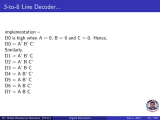
  • 14. 3-to-8 Line Decoder... implementation – D0 is high when A = 0, B = 0 and C = 0. Hence, D0 = A’ B’ C’ Similarly, D1 = A’ B’ C D2 = A’ B C’ D3 = A’ B C D4 = A B’ C’ D5 = A B’ C D6 = A B C’ D7 = A B C Dr. Nilesh Bhaskarrao Bahadure (Ph.D.) Digital Electronics July 1, 2021 14 / 135
  • 15. 3-to-8 Line Decoder... Figure : 3-to-8 Line Decoder Dr. Nilesh Bhaskarrao Bahadure (Ph.D.) Digital Electronics July 1, 2021 15 / 135
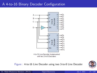
  • 16. 3-to-8 Line Decoder... Here a much larger 4 (3 data plus 1 enable) to 16 line binary decoder has been implemented using two smaller 3-to-8 decoders. Dr. Nilesh Bhaskarrao Bahadure (Ph.D.) Digital Electronics July 1, 2021 16 / 135
  • 17. A 4-to-16 Binary Decoder Configuration Figure : 4-to-16 Line Decoder using two 3-to-8 Line Decoder Dr. Nilesh Bhaskarrao Bahadure (Ph.D.) Digital Electronics July 1, 2021 17 / 135
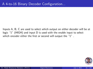
  • 18. A 4-to-16 Binary Decoder Configuration... Inputs A, B, C are used to select which output on either decoder will be at logic “1” (HIGH) and input D is used with the enable input to select which encoder either the first or second will output the “1” . Dr. Nilesh Bhaskarrao Bahadure (Ph.D.) Digital Electronics July 1, 2021 18 / 135
  • 19. BCD (Binary Coded Decimal) BCD (Binary Coded Decimal) is an encoding scheme which represents each of the decimal numbers by its equivalent 4-bit binary pattern. Seven segment displays comprise of seven individual segments formed by either Light Emitting Diodes (LEDs) or Liquid Crystal Displays (LCDs) arranged in a definite pattern (see Figure 8). Figure : Seven segment displays Dr. Nilesh Bhaskarrao Bahadure (Ph.D.) Digital Electronics July 1, 2021 19 / 135
  • 20. BCD (Binary Coded Decimal)... Two types of seven segment LED display: 1 Common Cathode Type: In this type of display all cathodes of the seven LEDs are connected together to the ground or -Vcc(hence,common cathode) and LED displays digits when some ’HIGH’ signal is supplied to the individual anodes. 2 Common Anode Type: In this type of display all the anodes of the seven LEDs are connected to battery or +Vcc and LED displays digits when some ’LOW’ signal is supplied to the individual cathodes. Dr. Nilesh Bhaskarrao Bahadure (Ph.D.) Digital Electronics July 1, 2021 20 / 135
  • 21. BCD (Binary Coded Decimal)... For the display to work, these segments are to be driven by the certain logic level at their input. Depending on this, seven segment displays are found to be of two types viz., common cathode type and common anode type. A common cathode display (Figure 9)(a) has all the cathode terminals of its LED segments tied together (green line). Further, this is grounded and hence is considered to be at logic 0 state. This means that in order to light up an LED, one needs to drive it high. On the other hand, a common anode display shown by Figure 9 (b) has all its anode terminals connected together which is further driven high by connecting it to a positive supply voltage (green line). Hence for this kind of display to work, one has to drive low on the cathode terminals of the individual LED segments. Dr. Nilesh Bhaskarrao Bahadure (Ph.D.) Digital Electronics July 1, 2021 21 / 135
  • 22. BCD (Binary Coded Decimal)... Figure : (a) Common cathod type display (b) Common anode type display Dr. Nilesh Bhaskarrao Bahadure (Ph.D.) Digital Electronics July 1, 2021 22 / 135
  • 23. BCD to seven segment decoder BCD to seven segment decoder is a circuit used to convert the input BCD into a form suitable for the display. It has four input lines (A, B, C and D) and 7 output lines (a, b, c, d, e, f and g) as shown in Figure 10. Considering common cathode type of arrangement, the truth table for the decoder can be given as in Table 4. Figure : BCD to seven segment decoder Dr. Nilesh Bhaskarrao Bahadure (Ph.D.) Digital Electronics July 1, 2021 23 / 135
  • 24. Table : Truth table for common cathode type BCD to seven segment decoder Dr. Nilesh Bhaskarrao Bahadure (Ph.D.) Digital Electronics July 1, 2021 24 / 135
  • 25. This table indicates the segments which are to be driven high to obtain certain decimal digit at the output of the seven segment display. However, it is to be noted that in the case of common anode type, the only change will be to interchange ones and zeros on the table. This means that from the truth table so obtained one can get to know where low has to be driven so as to obtain the required digit at the output. Dr. Nilesh Bhaskarrao Bahadure (Ph.D.) Digital Electronics July 1, 2021 25 / 135
  • 26. Digit A B C D a b c d e f g 0 0 0 0 0 0 0 0 0 0 0 1 1 0 0 0 1 1 0 0 1 1 1 1 2 0 0 1 0 0 0 1 0 0 1 0 3 0 0 1 1 0 0 0 0 1 1 0 4 0 1 0 0 1 0 0 1 1 0 0 5 0 1 0 1 0 1 0 0 1 0 0 6 0 1 1 0 0 1 0 0 0 0 0 7 0 1 1 1 0 0 0 1 1 1 1 8 1 0 0 0 0 0 0 0 0 0 0 9 1 0 0 1 0 0 0 0 1 0 0 Table : Truth table for common anode type BCD Dr. Nilesh Bhaskarrao Bahadure (Ph.D.) Digital Electronics July 1, 2021 26 / 135
  • 27. Design of BCD to 7 Segment Display Decoder Circuit The designing of BCD to seven segment display decoder circuit mainly involves four steps namely analysis, truth table design, K-map and designing a combinational logic circuit using logic gates. The first step of this circuit design is an analysis of the common cathode seven segment display. This display can be constructed with seven LEDs in the form of H. A truth table of this circuit can be designed by the inputs combinations for every decimal digit. For instance, decimal number ’1’ would control a blend of b & c. The second step is the truth table design by listing the display input signals-7, equivalent four-digit binary numbers as well as decimal number. Dr. Nilesh Bhaskarrao Bahadure (Ph.D.) Digital Electronics July 1, 2021 27 / 135
  • 28. The designing of the truth table for the decoder mainly depends on the kind of display. Already we have discussed above that is, for a common cathode display, the decoder output must be high in order to blink the segment. The tabular form of a BCD to 7-segment decoder with a common cathode display is shown below. The truth table consists of seven o/p columns equivalent to each of the seven segments. For example, the column for a-segment illustrates the various arrangements for which it is to be light up. Thus ’a’- segment is energetic for the digits like 0, 2, 3, 5, 6, 7, 8 & 9. Dr. Nilesh Bhaskarrao Bahadure (Ph.D.) Digital Electronics July 1, 2021 28 / 135
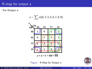
  • 29. K-map for output a For Output a: a = X m(0, 2, 3, 5, 6, 7, 8, 9) Figure : K-Map for Output a Dr. Nilesh Bhaskarrao Bahadure (Ph.D.) Digital Electronics July 1, 2021 29 / 135
  • 30. K-map for output b For Output b: b = X m(0, 1, 2, 3, 4, 7, 8, 9) Figure : K-Map for Output b Dr. Nilesh Bhaskarrao Bahadure (Ph.D.) Digital Electronics July 1, 2021 30 / 135
  • 31. K-map for output c For Output c: c = X m(0, 1, 3, 4, 5, 6, 7, 8, 9) Figure : K-Map for Output c Dr. Nilesh Bhaskarrao Bahadure (Ph.D.) Digital Electronics July 1, 2021 31 / 135
  • 32. K-map for output d For Output d: d = X m(0, 2, 3, 5, 6, 8, 9) Figure : K-Map for Output d Dr. Nilesh Bhaskarrao Bahadure (Ph.D.) Digital Electronics July 1, 2021 32 / 135
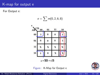
  • 33. K-map for output e For Output e: e = X m(0, 2, 6, 8) Figure : K-Map for Output e Dr. Nilesh Bhaskarrao Bahadure (Ph.D.) Digital Electronics July 1, 2021 33 / 135
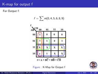
  • 34. K-map for output f For Output f: f = X m(0, 4, 5, 6, 8, 9) Figure : K-Map for Output f Dr. Nilesh Bhaskarrao Bahadure (Ph.D.) Digital Electronics July 1, 2021 34 / 135
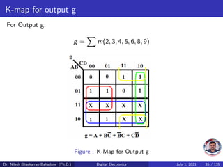
  • 35. K-map for output g For Output g: g = X m(2, 3, 4, 5, 6, 8, 9) Figure : K-Map for Output g Dr. Nilesh Bhaskarrao Bahadure (Ph.D.) Digital Electronics July 1, 2021 35 / 135
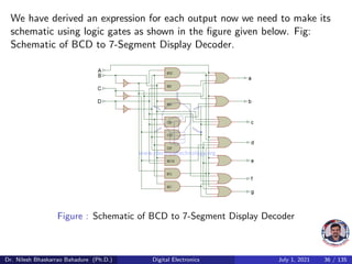
  • 36. We have derived an expression for each output now we need to make its schematic using logic gates as shown in the figure given below. Fig: Schematic of BCD to 7-Segment Display Decoder. Figure : Schematic of BCD to 7-Segment Display Decoder Dr. Nilesh Bhaskarrao Bahadure (Ph.D.) Digital Electronics July 1, 2021 36 / 135
  • 37. Encoders The encoders and decoders play an essential role in digital electronics projects; encoders decoders are used to convert data from one form to another form. These are frequently used in communication system such as telecommunication, networking, etc..to transfer data from one end to the other end. Similarly, in the digital domain, for easy transmission of data, it is often encrypted or placed within codes, and then transmitted. At the receiver, the coded data is decrypted or gathered from the code and is processed in order to be displayed or given to the load accordingly. Dr. Nilesh Bhaskarrao Bahadure (Ph.D.) Digital Electronics July 1, 2021 37 / 135
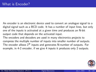
  • 38. What is Encoder? An encoder is an electronic device used to convert an analogue signal to a digital signal such as a BCD code. It has a number of input lines, but only one of the inputs is activated at a given time and produces an N-bit output code that depends on the activated input. The encoders and decoders are used in many electronics projects to compress the multiple number of inputs into smaller number of outputs. The encoder allows 2N inputs and generates N-number of outputs. For example, in 4-2 encoder, if we give 4 inputs it produces only 2 outputs. Dr. Nilesh Bhaskarrao Bahadure (Ph.D.) Digital Electronics July 1, 2021 38 / 135
  • 39. Figure : Logic Symbol of Encoder An Encoder is a Combinational circuit that performs the reverse operation of Decoder. It has maximum of 2n input lines and ’n’ output lines. It will produce a binary code equivalent to the input, which is active High. Therefore, the encoder encodes 2n input lines with ’n’ bits. It is optional to represent the enable signal in encoders. Dr. Nilesh Bhaskarrao Bahadure (Ph.D.) Digital Electronics July 1, 2021 39 / 135
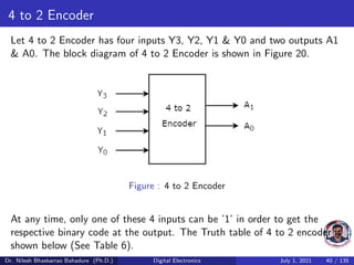
  • 40. 4 to 2 Encoder Let 4 to 2 Encoder has four inputs Y3, Y2, Y1 & Y0 and two outputs A1 & A0. The block diagram of 4 to 2 Encoder is shown in Figure 20. Figure : 4 to 2 Encoder At any time, only one of these 4 inputs can be ’1’ in order to get the respective binary code at the output. The Truth table of 4 to 2 encoder is shown below (See Table 6). Dr. Nilesh Bhaskarrao Bahadure (Ph.D.) Digital Electronics July 1, 2021 40 / 135
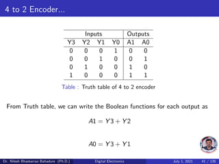
  • 41. 4 to 2 Encoder... Inputs Outputs Y3 Y2 Y1 Y0 A1 A0 0 0 0 1 0 0 0 0 1 0 0 1 0 1 0 0 1 0 1 0 0 0 1 1 Table : Truth table of 4 to 2 encoder From Truth table, we can write the Boolean functions for each output as A1 = Y 3 + Y 2 A0 = Y 3 + Y 1 Dr. Nilesh Bhaskarrao Bahadure (Ph.D.) Digital Electronics July 1, 2021 41 / 135
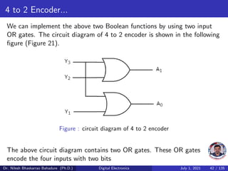
  • 42. 4 to 2 Encoder... We can implement the above two Boolean functions by using two input OR gates. The circuit diagram of 4 to 2 encoder is shown in the following figure (Figure 21). Figure : circuit diagram of 4 to 2 encoder The above circuit diagram contains two OR gates. These OR gates encode the four inputs with two bits Dr. Nilesh Bhaskarrao Bahadure (Ph.D.) Digital Electronics July 1, 2021 42 / 135
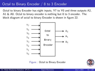
  • 43. Octal to Binary Encoder / 8 to 3 Encoder Octal to binary Encoder has eight inputs, Y7 to Y0 and three outputs A2, A1 & A0. Octal to binary encoder is nothing but 8 to 3 encoder. The block diagram of octal to binary Encoder is shown in figure 22. Figure : Octal to Binary Encoder Dr. Nilesh Bhaskarrao Bahadure (Ph.D.) Digital Electronics July 1, 2021 43 / 135
  • 44. Octal to Binary Encoder / 8 to 3 Encoder... At any time, only one of these eight inputs can be ’1’ in order to get the respective binary code. The Truth table of octal to binary encoder is shown below. Inputs Outputs Y7 Y6 Y5 Y4 Y3 Y2 Y1 Y0 A2 A1 A0 0 0 0 0 0 0 0 1 0 0 0 0 0 0 0 0 0 1 0 0 0 1 0 0 0 0 0 1 0 0 0 1 0 0 0 0 0 1 0 0 0 0 1 1 0 0 0 1 0 0 0 0 1 0 0 0 0 1 0 0 0 0 0 1 0 1 0 1 0 0 0 0 0 0 1 1 0 1 0 0 0 0 0 0 0 1 1 1 Table : Truth table of octal to binary encoder Dr. Nilesh Bhaskarrao Bahadure (Ph.D.) Digital Electronics July 1, 2021 44 / 135
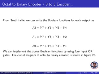
  • 45. Octal to Binary Encoder / 8 to 3 Encoder... From Truth table, we can write the Boolean functions for each output as A2 = Y 7 + Y 6 + Y 5 + Y 4 A1 = Y 7 + Y 6 + Y 3 + Y 2 A0 = Y 7 + Y 5 + Y 3 + Y 1 We can implement the above Boolean functions by using four input OR gates. The circuit diagram of octal to binary encoder is shown in figure 23. Dr. Nilesh Bhaskarrao Bahadure (Ph.D.) Digital Electronics July 1, 2021 45 / 135
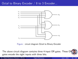
  • 46. Octal to Binary Encoder / 8 to 3 Encoder... Figure : circuit diagram Octal to Binary Encoder The above circuit diagram contains three 4-input OR gates. These OR gates encode the eight inputs with three bits. Dr. Nilesh Bhaskarrao Bahadure (Ph.D.) Digital Electronics July 1, 2021 46 / 135
  • 47. Drawbacks of Encoder Following are the drawbacks of normal encoder. 1 There is an ambiguity, when all outputs of encoder are equal to zero. Because, it could be the code corresponding to the inputs, when only least significant input is one or when all inputs are zero. 2 If more than one input is active High, then the encoder produces an output, which may not be the correct code. For example, if both Y3 and Y6 are ’1’, then the encoder produces 111 at the output. This is neither equivalent code corresponding to Y3, when it is ’1’ nor the equivalent code corresponding to Y6, when it is ’1’. So, to overcome these difficulties, we should assign priorities to each input of encoder. Then, the output of encoder will be the binary code corresponding to the active High inputs, which has higher priority. This encoder is called as priority encoder. Dr. Nilesh Bhaskarrao Bahadure (Ph.D.) Digital Electronics July 1, 2021 47 / 135
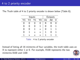
  • 48. Priority Encoder A 4 to 2 priority encoder has four inputs Y3, Y2, Y1 & Y0 and two outputs A1 & A0. Here, the input, Y3 has the highest priority, whereas the input, Y0 has the lowest priority. In this case, even if more than one input is ’1’ at the same time, the output will be the binary code corresponding to the input, which is having higher priority. We considered one more output, V in order to know, whether the code available at outputs is valid or not. 1 If at least one input of the encoder is ’1’, then the code available at outputs is a valid one. In this case, the output, V will be equal to 1. 2 If all the inputs of encoder are ’0’, then the code available at outputs is not a valid one. In this case, the output, V will be equal to 0. The other two outputs are not inspected when V equals 0 and are specified as don’t-care conditions. Dr. Nilesh Bhaskarrao Bahadure (Ph.D.) Digital Electronics July 1, 2021 48 / 135
  • 49. 4 to 2 priority encoder The Truth table of 4 to 2 priority encoder is shown below (Table 8). Inputs Outputs Y3 Y2 Y1 Y0 A1 A0 V 0 0 0 0 X X 0 0 0 0 1 0 0 1 0 0 1 x 0 1 1 0 1 x x 1 0 1 1 x x x 1 1 1 Table : 4 to 2 priority encoder Instead of listing all 16 minterms of four variables, the truth table uses an X to represent either 1 or 0. For example, X100 represents the two minterms 0100 and 1100 Dr. Nilesh Bhaskarrao Bahadure (Ph.D.) Digital Electronics July 1, 2021 49 / 135
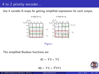
  • 50. 4 to 2 priority encoder... Use 4 variable K-maps for getting simplified expressions for each output. Figure : The simplified Boolean functions are A1 = Y 3 + Y 2 A0 = Y 3 + ¯ Y 2Y 1 Dr. Nilesh Bhaskarrao Bahadure (Ph.D.) Digital Electronics July 1, 2021 50 / 135
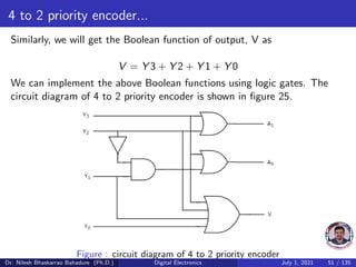
  • 51. 4 to 2 priority encoder... Similarly, we will get the Boolean function of output, V as V = Y 3 + Y 2 + Y 1 + Y 0 We can implement the above Boolean functions using logic gates. The circuit diagram of 4 to 2 priority encoder is shown in figure 25. Figure : circuit diagram of 4 to 2 priority encoder Dr. Nilesh Bhaskarrao Bahadure (Ph.D.) Digital Electronics July 1, 2021 51 / 135
  • 52. The above circuit diagram (figure 25) contains two 2-input OR gates, one 4-input OR gate, one 2 input AND gate & an inverter. Here AND gate & inverter combination are used for producing a valid code at the outputs, even when multiple inputs are equal to ’1’ at the same time. Hence, this circuit encodes the four inputs with two bits based on the priority assigned to each input. Dr. Nilesh Bhaskarrao Bahadure (Ph.D.) Digital Electronics July 1, 2021 52 / 135
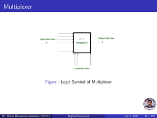
  • 53. What is Multiplexer? Multiplexer is a device that has multiple inputs and a single line output. The select lines determine which input is connected to the output. Multiplexer is a Combinational circuit that has maximum of 2n data inputs, ’n’ selection lines and single output line. One of these data inputs will be connected to the output based on the values of selection lines. Since there are ’n’ selection lines, there will be 2n possible combinations of zeros and ones. So, each combination will select only one data input. Multiplexer is also called as Mux. It is also called a data selector. Dr. Nilesh Bhaskarrao Bahadure (Ph.D.) Digital Electronics July 1, 2021 53 / 135
  • 54. Multiplexer Figure : Logic Symbol of Multiplexer Dr. Nilesh Bhaskarrao Bahadure (Ph.D.) Digital Electronics July 1, 2021 54 / 135
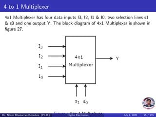
  • 55. 4 to 1 Multiplexer 4x1 Multiplexer has four data inputs I3, I2, I1 & I0, two selection lines s1 & s0 and one output Y. The block diagram of 4x1 Multiplexer is shown in figure 27. Figure : 4 to 1 Multiplexer Dr. Nilesh Bhaskarrao Bahadure (Ph.D.) Digital Electronics July 1, 2021 55 / 135
  • 56. 4 to 1 Multiplexer One of these 4 inputs will be connected to the output based on the combination of inputs present at these two selection lines. Truth table of 4x1 Multiplexer is shown below (Table 9). Selection Lines Output S1 S0 Y 0 0 I0 0 1 I1 1 0 I2 1 1 I3 Table : Truth table of 4x1 Multiplexer From Truth table, we can directly write the Boolean function for output, Y as Y = S10 S00 I0 + S10 S0I1 + S1S00 I2 + S1S0I3 Dr. Nilesh Bhaskarrao Bahadure (Ph.D.) Digital Electronics July 1, 2021 56 / 135
  • 57. 4 to 1 Multiplexer We can implement this Boolean function using Inverters, AND gates & OR gate. The circuit diagram of 4x1 multiplexer is shown in figure 28. Figure : circuit diagram of 4x1 multiplexer We can easily understand the operation of the above circuit. Similarly, you can implement 8x1 Multiplexer and 16x1 multiplexer by following the same procedure. Dr. Nilesh Bhaskarrao Bahadure (Ph.D.) Digital Electronics July 1, 2021 57 / 135
  • 58. Implementation of Higher-order Multiplexers. Now, let us implement the following two higher-order Multiplexers using lower-order Multiplexers. 1 8x1 Multiplexer 2 16x1 Multiplexer Dr. Nilesh Bhaskarrao Bahadure (Ph.D.) Digital Electronics July 1, 2021 58 / 135
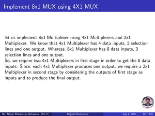
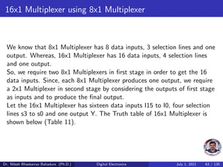
  • 59. Implement 8x1 MUX using 4X1 MUX let us implement 8x1 Multiplexer using 4x1 Multiplexers and 2x1 Multiplexer. We know that 4x1 Multiplexer has 4 data inputs, 2 selection lines and one output. Whereas, 8x1 Multiplexer has 8 data inputs, 3 selection lines and one output. So, we require two 4x1 Multiplexers in first stage in order to get the 8 data inputs. Since, each 4x1 Multiplexer produces one output, we require a 2x1 Multiplexer in second stage by considering the outputs of first stage as inputs and to produce the final output. Dr. Nilesh Bhaskarrao Bahadure (Ph.D.) Digital Electronics July 1, 2021 59 / 135
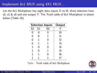
  • 60. Implement 8x1 MUX using 4X1 MUX... Let the 8x1 Multiplexer has eight data inputs I7 to I0, three selection lines s2, s1 & s0 and one output Y. The Truth table of 8x1 Multiplexer is shown below (Table 10). Selection Inputs Output S2 S1 S0 Y 0 0 0 I0 0 0 1 I1 0 1 0 I2 0 1 1 I3 1 0 0 I4 1 0 1 I5 1 1 0 I6 1 1 1 I7 Table : Truth table of 8x1 Multiplexer Dr. Nilesh Bhaskarrao Bahadure (Ph.D.) Digital Electronics July 1, 2021 60 / 135
  • 61. Implement 8x1 MUX using 4X1 MUX... We can implement 8x1 Multiplexer using lower order Multiplexers easily by considering the above Truth table. The block diagram of 8x1 Multiplexer is shown in figure 29. Figure : circuit diagram of 8x1 Multiplexer using 4x1 multiplexer Dr. Nilesh Bhaskarrao Bahadure (Ph.D.) Digital Electronics July 1, 2021 61 / 135
  • 62. Implement 8x1 MUX using 4X1 MUX... The same selection lines, s1 & s0 are applied to both 4x1 Multiplexers. The data inputs of upper 4x1 Multiplexer are I7 to I4 and the data inputs of lower 4x1 Multiplexer are I3 to I0. Therefore, each 4x1 Multiplexer produces an output based on the values of selection lines, s1 & s0. The outputs of first stage 4x1 Multiplexers are applied as inputs of 2x1 Multiplexer that is present in second stage. The other selection line, s2 is applied to 2x1 Multiplexer. 1 If s2 is zero, then the output of 2x1 Multiplexer will be one of the 4 inputs I3 to I0 based on the values of selection lines s1 & s0. 2 If s2 is one, then the output of 2x1 Multiplexer will be one of the 4 inputs I7 to I4 based on the values of selection lines s1 & s0. Therefore, the overall combination of two 4x1 Multiplexers and one 2x1 Multiplexer performs as one 8x1 Multiplexer. Dr. Nilesh Bhaskarrao Bahadure (Ph.D.) Digital Electronics July 1, 2021 62 / 135
  • 63. 16x1 Multiplexer using 8x1 Multiplexer We know that 8x1 Multiplexer has 8 data inputs, 3 selection lines and one output. Whereas, 16x1 Multiplexer has 16 data inputs, 4 selection lines and one output. So, we require two 8x1 Multiplexers in first stage in order to get the 16 data inputs. Since, each 8x1 Multiplexer produces one output, we require a 2x1 Multiplexer in second stage by considering the outputs of first stage as inputs and to produce the final output. Let the 16x1 Multiplexer has sixteen data inputs I15 to I0, four selection lines s3 to s0 and one output Y. The Truth table of 16x1 Multiplexer is shown below (Table 11). Dr. Nilesh Bhaskarrao Bahadure (Ph.D.) Digital Electronics July 1, 2021 63 / 135
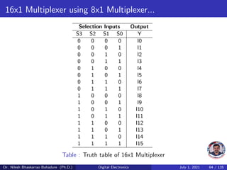
  • 64. 16x1 Multiplexer using 8x1 Multiplexer... Selection Inputs Output S3 S2 S1 S0 Y 0 0 0 0 I0 0 0 0 1 I1 0 0 1 0 I2 0 0 1 1 I3 0 1 0 0 I4 0 1 0 1 I5 0 1 1 0 I6 0 1 1 1 I7 1 0 0 0 I8 1 0 0 1 I9 1 0 1 0 I10 1 0 1 1 I11 1 1 0 0 I12 1 1 0 1 I13 1 1 1 0 I14 1 1 1 1 I15 Table : Truth table of 16x1 Multiplexer Dr. Nilesh Bhaskarrao Bahadure (Ph.D.) Digital Electronics July 1, 2021 64 / 135
  • 65. 16x1 Multiplexer using 8x1 Multiplexer... We can implement 16x1 Multiplexer using lower order Multiplexers easily by considering the above Truth table. The block diagram of 16x1 Multiplexer is shown in figure 30. Figure : circuit diagram of 16x1 Multiplexer using 8x1 multiplexer Dr. Nilesh Bhaskarrao Bahadure (Ph.D.) Digital Electronics July 1, 2021 65 / 135
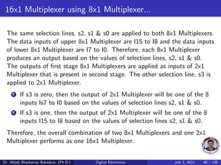
  • 66. 16x1 Multiplexer using 8x1 Multiplexer... The same selection lines, s2, s1 & s0 are applied to both 8x1 Multiplexers. The data inputs of upper 8x1 Multiplexer are I15 to I8 and the data inputs of lower 8x1 Multiplexer are I7 to I0. Therefore, each 8x1 Multiplexer produces an output based on the values of selection lines, s2, s1 & s0. The outputs of first stage 8x1 Multiplexers are applied as inputs of 2x1 Multiplexer that is present in second stage. The other selection line, s3 is applied to 2x1 Multiplexer. 1 If s3 is zero, then the output of 2x1 Multiplexer will be one of the 8 inputs Is7 to I0 based on the values of selection lines s2, s1 & s0. 2 If s3 is one, then the output of 2x1 Multiplexer will be one of the 8 inputs I15 to I8 based on the values of selection lines s2, s1 & s0. Therefore, the overall combination of two 8x1 Multiplexers and one 2x1 Multiplexer performs as one 16x1 Multiplexer. Dr. Nilesh Bhaskarrao Bahadure (Ph.D.) Digital Electronics July 1, 2021 66 / 135
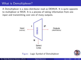
  • 67. What is Demultiplexer? A Demultiplexer is a data distributor read as DEMUX. It is quite opposite to multiplexer or MUX. It is a process of taking information from one input and transmitting over one of many outputs. Figure : Logic Symbol of Demultiplexer Dr. Nilesh Bhaskarrao Bahadure (Ph.D.) Digital Electronics July 1, 2021 67 / 135
  • 68. What is Demultiplexer?... DEMUX are used to implement general-purpose logic systems. A demultiplexer takes one single input data line and distributes it to any one of a number of individual output lines one at a time. Demultiplexing is the process of converting a signal containing multiple analog or digital signals backs into the original and separate signals. A demultiplexer of 2n outputs has n select lines. Dr. Nilesh Bhaskarrao Bahadure (Ph.D.) Digital Electronics July 1, 2021 68 / 135
  • 69. 1x4 De-Multiplexer A 1-to-4 demultiplexer has a single input (D), two selection lines (S1 and S0) and four outputs (Y0 to Y3). The input data goes to any one of the four outputs at a given time for a particular combination of select lines. The block diagram of 1x4 De-Multiplexer is shown in figure 32. Figure : block diagram of 1x4 De-Multiplexer Dr. Nilesh Bhaskarrao Bahadure (Ph.D.) Digital Electronics July 1, 2021 69 / 135
  • 70. 1x4 De-Multiplexer... The truth table of this type of demultiplexer is given below (Table ??). From the truth table it is clear that, when S1=0 and S0= 0, the data input is connected to output Y0 and when S1= 0 and s0=1, then the data input is connected to output Y1. Data Input Selection Inputs Outputs Din S1 S0 Y3 Y2 Y1 Y0 D 0 0 0 0 0 D D 0 1 0 0 D 0 D 1 0 0 D 0 0 D 1 1 D 0 0 0 Table : Truth table for 1 to 4 DMUX Dr. Nilesh Bhaskarrao Bahadure (Ph.D.) Digital Electronics July 1, 2021 70 / 135
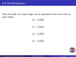
  • 71. 1x4 De-Multiplexer... From the table, the output logic can be expressed as min terms and are given below. Y0 = ¯ S1 ¯ S0D Y1 = ¯ S1S0D Y2 = S1 ¯ S0D Y3 = S1S0D Dr. Nilesh Bhaskarrao Bahadure (Ph.D.) Digital Electronics July 1, 2021 71 / 135
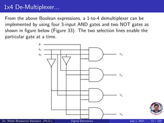
  • 72. 1x4 De-Multiplexer... From the above Boolean expressions, a 1-to-4 demultiplexer can be implemented by using four 3-input AND gates and two NOT gates as shown in figure below (Figure 33). The two selection lines enable the particular gate at a time. Dr. Nilesh Bhaskarrao Bahadure (Ph.D.) Digital Electronics July 1, 2021 72 / 135
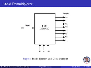
  • 73. 1-to-8 Demultiplexer The below figure shows the block diagram of a 1-to-8 demultiplexer that consists of single input D, three select inputs S2, S1 and S0 and eight outputs from Y0 to Y7. It is also called as 3-to-8 demultiplexer due to three select input lines. It distributes one input line to one of 8 output lines depending on the combination of select inputs. Dr. Nilesh Bhaskarrao Bahadure (Ph.D.) Digital Electronics July 1, 2021 73 / 135
  • 74. 1-to-8 Demultiplexer... Figure : Block diagram 1x8 De-Multiplexer Dr. Nilesh Bhaskarrao Bahadure (Ph.D.) Digital Electronics July 1, 2021 74 / 135
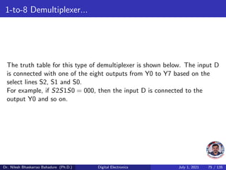
  • 75. 1-to-8 Demultiplexer... The truth table for this type of demultiplexer is shown below. The input D is connected with one of the eight outputs from Y0 to Y7 based on the select lines S2, S1 and S0. For example, if S2S1S0 = 000, then the input D is connected to the output Y0 and so on. Dr. Nilesh Bhaskarrao Bahadure (Ph.D.) Digital Electronics July 1, 2021 75 / 135
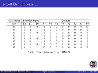
  • 76. 1-to-8 Demultiplexer... Data Input Selection Inputs Outputs Din S2 S1 S0 Y7 Y6 Y5 Y4 Y3 Y2 Y1 Y0 D 0 0 0 0 0 0 0 0 0 0 D D 0 0 1 0 0 0 0 0 0 D 0 D 0 1 0 0 0 0 0 0 D 0 0 D 0 1 1 0 0 0 0 D 0 0 0 D 1 0 0 0 0 0 D 0 0 0 0 D 1 0 1 0 0 D 0 0 0 0 0 D 1 1 0 0 D 0 0 0 0 0 0 D 1 1 1 D 0 0 0 0 0 0 0 Table : Truth table for 1 to 8 DMUX Dr. Nilesh Bhaskarrao Bahadure (Ph.D.) Digital Electronics July 1, 2021 76 / 135
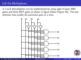
  • 77. 1x8 De-Multiplexer... A 1-to-8 demultiplexer can be implemented by using eight 4-input AND gates and three NOT gates as shown in figure below (Figure 35). The two selection lines enable the particular gate at a time. Dr. Nilesh Bhaskarrao Bahadure (Ph.D.) Digital Electronics July 1, 2021 77 / 135
  • 78. Implementation of Higher-order De-Multiplexers Now, let us implement the following two higher-order De-Multiplexers using lower-order De-Multiplexers. 1 1x8 De-Multiplexer 2 1x16 De-Multiplexer Dr. Nilesh Bhaskarrao Bahadure (Ph.D.) Digital Electronics July 1, 2021 78 / 135
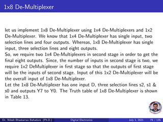
  • 79. 1x8 De-Multiplexer let us implement 1x8 De-Multiplexer using 1x4 De-Multiplexers and 1x2 De-Multiplexer. We know that 1x4 De-Multiplexer has single input, two selection lines and four outputs. Whereas, 1x8 De-Multiplexer has single input, three selection lines and eight outputs. So, we require two 1x4 De-Multiplexers in second stage in order to get the final eight outputs. Since, the number of inputs in second stage is two, we require 1x2 DeMultiplexer in first stage so that the outputs of first stage will be the inputs of second stage. Input of this 1x2 De-Multiplexer will be the overall input of 1x8 De-Multiplexer. Let the 1x8 De-Multiplexer has one input D, three selection lines s2, s1 & s0 and outputs Y7 to Y0. The Truth table of 1x8 De-Multiplexer is shown in Table 13. Dr. Nilesh Bhaskarrao Bahadure (Ph.D.) Digital Electronics July 1, 2021 79 / 135
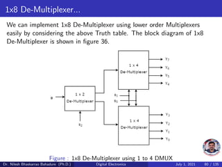
  • 80. 1x8 De-Multiplexer... We can implement 1x8 De-Multiplexer using lower order Multiplexers easily by considering the above Truth table. The block diagram of 1x8 De-Multiplexer is shown in figure 36. Figure : 1x8 De-Multiplexer using 1 to 4 DMUX Dr. Nilesh Bhaskarrao Bahadure (Ph.D.) Digital Electronics July 1, 2021 80 / 135
  • 81. The common selection lines, s1 & s0 are applied to both 1x4 De-Multiplexers. The outputs of upper 1x4 De-Multiplexer are Y7 to Y4 and the outputs of lower 1x4 De-Multiplexer are Y3 to Y0. The other selection line, s2 is applied to 1x2 De-Multiplexer. If s2 is zero, then one of the four outputs of lower 1x4 De-Multiplexer will be equal to input, D based on the values of selection lines s1 & s0. Similarly, if s2 is one, then one of the four outputs of upper 1x4 DeMultiplexer will be equal to input, D based on the values of selection lines s1 & s0. Dr. Nilesh Bhaskarrao Bahadure (Ph.D.) Digital Electronics July 1, 2021 81 / 135
  • 82. 1 to 16 DMUX Dr. Nilesh Bhaskarrao Bahadure (Ph.D.) Digital Electronics July 1, 2021 82 / 135
  • 83. How to implement any Boolean function using MUX? While implementing any function using MUX, if we have N variables in the function then we take (N-1) variables on the selection lines and 1 variable is used for inputs of MUX. As we have N-1 variables on selection lines we need to have 2 N-1 to 1 MUX. We just have to connect A, A’, 0 or 1 to different input lines. Dr. Nilesh Bhaskarrao Bahadure (Ph.D.) Digital Electronics July 1, 2021 83 / 135
  • 84. Example - 1 Question To implement the function F(A, B, C)= (1, 2, 5, 7) using 1 8 to 1 MUX 2 4 to 1 MUX Dr. Nilesh Bhaskarrao Bahadure (Ph.D.) Digital Electronics July 1, 2021 84 / 135
  • 85. Example 1: Solution Solution Part - I: We can implement it using all three variables at selection lines. We put 1 on the min term lines which are present in functions and 0 on the rest. Figure : Implementation of Boolean function using 8 to 1 MUX Dr. Nilesh Bhaskarrao Bahadure (Ph.D.) Digital Electronics July 1, 2021 85 / 135
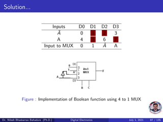
  • 86. Solution... Part - II: F= A’B’C + A’BC’ + AB’C + ABC N=3 so we use 2 N-1 = 2 2 = 4 to 1 MUX. Suppose we have B, C on the selection lines. So when we have BC=00, put B=0, C=0 in the function and we see output of the function should be 0 hence we connect 0 to 0th input line. When BC=01, then output of the function should be A’+ A = 1. Hence we connect 1 to 1st line. When BC=10, then output of the function should be A’. Hence we connect A’ to 2nd line. When BC=11, then output of the function should be A. Hence we connect A to 3rd line. Hence we have the circuit as Dr. Nilesh Bhaskarrao Bahadure (Ph.D.) Digital Electronics July 1, 2021 86 / 135
  • 87. Solution... Inputs D0 D1 D2 D3 Ā 0 1 2 3 A 4 5 6 7 Input to MUX 0 1 Ā A Figure : Implementation of Boolean function using 4 to 1 MUX Dr. Nilesh Bhaskarrao Bahadure (Ph.D.) Digital Electronics July 1, 2021 87 / 135
  • 88. To implement the function F(A, B, C)= (1, 2, 5, 7) using MUX using different variable as selection variable. Solution: Let’s now take the variable B for input lines and A & C for selection lines. The min terms with B in compliment form are 0, 1, 4, 5 and the min terms with B in un-complimented form are 2, 3, 6, 7 Inputs D0 D1 D2 D3 B̄ 0 1 4 5 B 2 3 6 7 Input to MUX B B̄ 0 1 Figure : Implementation of Boolean function using 4 to 1 MUX Dr. Nilesh Bhaskarrao Bahadure (Ph.D.) Digital Electronics July 1, 2021 88 / 135
  • 89. Example - 2 Question To implement the function f ( A, B, C) = ( 1, 2, 3, 5, 6 ) with don’t care (7) using 4 to 1 MUX Dr. Nilesh Bhaskarrao Bahadure (Ph.D.) Digital Electronics July 1, 2021 89 / 135
  • 90. Solution A B C f 0 0 0 C’ 0 0 1 C 0 1 0 C’ 0 1 1 C 1 0 0 C’ 1 0 1 C 1 1 0 C’ 1 1 1 C Dr. Nilesh Bhaskarrao Bahadure (Ph.D.) Digital Electronics July 1, 2021 90 / 135
  • 91. Solution Inputs D0 D1 D2 D3 C̄ 0 2 4 6 C 1 3 5 7 Input to MUX C 1 C 1 Note: If don’t care term is consider then 1 otherwise C’ is connected to the input D3. Figure : Implementation of Boolean function using 4 to 1 MUX Dr. Nilesh Bhaskarrao Bahadure (Ph.D.) Digital Electronics July 1, 2021 91 / 135
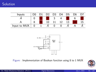
  • 92. Example - 3 Question To implement the function F(A, B, C, D)= (1, 2, 5, 7, 9, 14) using 8 to 1 MUX using variable A as input line. Dr. Nilesh Bhaskarrao Bahadure (Ph.D.) Digital Electronics July 1, 2021 92 / 135
  • 93. Solution Inputs D0 D1 D2 D3 D4 D5 D6 D7 Ā 0 1 2 3 4 5 6 7 A 8 9 10 11 12 13 14 15 Input to MUX 0 1 Ā 0 0 Ā A Ā Figure : Implementation of Boolean function using 8 to 1 MUX Dr. Nilesh Bhaskarrao Bahadure (Ph.D.) Digital Electronics July 1, 2021 93 / 135
  • 94. Example - 4 Question To implement the function F(A, B, C, D)= (0,1,4,5,6,8,10,12,13) using 8 to 1 MUX using variable A as input line. Dr. Nilesh Bhaskarrao Bahadure (Ph.D.) Digital Electronics July 1, 2021 94 / 135
  • 95. Solution Inputs D0 D1 D2 D3 D4 D5 D6 D7 Ā 0 1 2 3 4 5 6 7 A 8 9 10 11 12 13 14 15 Input to MUX 1 Ā A 0 1 1 Ā 0 Figure : Implementation of Boolean function using 8 to 1 MUX Dr. Nilesh Bhaskarrao Bahadure (Ph.D.) Digital Electronics July 1, 2021 95 / 135
  • 96. Example - 5 Question To implement the function F(A, B, C) = ĀB + BC + ĀC using 4 to 1 MUX using variable C as input line. Dr. Nilesh Bhaskarrao Bahadure (Ph.D.) Digital Electronics July 1, 2021 96 / 135
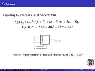
  • 97. Solution Expanding to standard sum of products form: F(A, B, C) = ĀB(C + C̄) + (A + Ā)BC + Ā(B + B̄)C F(A, B, C) = ĀBC + ĀBC̄ + ĀB̄C + ABC Figure : Implementation of Boolean function using 4 to 1 MUX Dr. Nilesh Bhaskarrao Bahadure (Ph.D.) Digital Electronics July 1, 2021 97 / 135
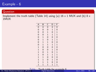
  • 98. Example - 6 Question Implement the truth table (Table 14) using (a) 16 x 1 MUX and (b) 8 x 1MUX A B C D F 0 0 0 0 0 0 0 0 1 0 0 0 1 0 1 0 0 1 1 1 0 1 0 0 0 0 1 0 1 1 0 1 1 0 0 0 1 1 1 1 1 0 0 0 0 1 0 0 1 0 1 0 1 0 1 1 0 1 1 1 1 1 0 0 0 1 1 0 1 0 1 1 1 0 0 1 1 1 1 1 Table : Truth table for example 6 Dr. Nilesh Bhaskarrao Bahadure (Ph.D.) Digital Electronics July 1, 2021 98 / 135
  • 99. Solution Part - I: Figure : Implementation using 16 x 1 MUX Dr. Nilesh Bhaskarrao Bahadure (Ph.D.) Digital Electronics July 1, 2021 99 / 135
  • 100. Solution... Part - II: Inputs D0 D1 D2 D3 D4 D5 D6 D7 D̄ 0 2 4 6 8 10 12 14 D 1 3 5 7 9 11 13 15 Input to MUX 0 1 D D 0 1 0 D Figure : Implementation of Boolean function using 8 to 1 MUX Dr. Nilesh Bhaskarrao Bahadure (Ph.D.) Digital Electronics July 1, 2021 100 / 135
  • 101. Binary Adder The most basic arithmetic operation is addition. The circuit, which performs the addition of two binary numbers is known as Binary adder. First, let us implement an adder, which performs the addition of two bits. Dr. Nilesh Bhaskarrao Bahadure (Ph.D.) Digital Electronics July 1, 2021 101 / 135
  • 102. Half Adder Half adder is a combinational circuit, which performs the addition of two binary numbers A and B are of single bit. It produces two outputs sum, S & carry, C. The logic Symbol of half adder circuit is shown in figure 47. Figure : Symbol of half adder circuit Dr. Nilesh Bhaskarrao Bahadure (Ph.D.) Digital Electronics July 1, 2021 102 / 135
  • 103. Half Adder... The Truth table of Half adder is shown below. Inputs Outputs A B Sum (S) Carry 0 0 0 0 0 1 1 0 1 0 1 0 1 1 0 1 Table : Truth table of Half adder When we do the addition of two bits, the resultant sum can have the values ranging from 0 to 2 in decimal. We can represent the decimal digits 0 and 1 with single bit in binary. But, we cant represent decimal digit 2 with single bit in binary. So, we require two bits for representing it in binary. Dr. Nilesh Bhaskarrao Bahadure (Ph.D.) Digital Electronics July 1, 2021 103 / 135
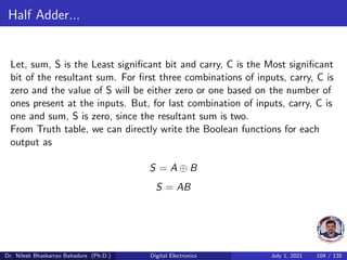
  • 104. Half Adder... Let, sum, S is the Least significant bit and carry, C is the Most significant bit of the resultant sum. For first three combinations of inputs, carry, C is zero and the value of S will be either zero or one based on the number of ones present at the inputs. But, for last combination of inputs, carry, C is one and sum, S is zero, since the resultant sum is two. From Truth table, we can directly write the Boolean functions for each output as S = A ⊕ B S = AB Dr. Nilesh Bhaskarrao Bahadure (Ph.D.) Digital Electronics July 1, 2021 104 / 135
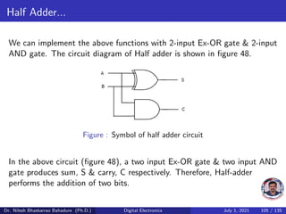
  • 105. Half Adder... We can implement the above functions with 2-input Ex-OR gate & 2-input AND gate. The circuit diagram of Half adder is shown in figure 48. Figure : Symbol of half adder circuit In the above circuit (figure 48), a two input Ex-OR gate & two input AND gate produces sum, S & carry, C respectively. Therefore, Half-adder performs the addition of two bits. Dr. Nilesh Bhaskarrao Bahadure (Ph.D.) Digital Electronics July 1, 2021 105 / 135
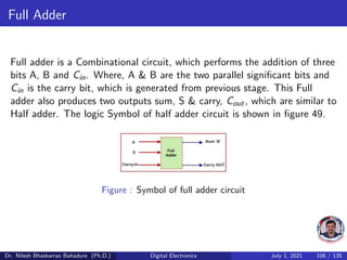
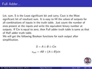
  • 106. Full Adder Full adder is a Combinational circuit, which performs the addition of three bits A, B and Cin. Where, A & B are the two parallel significant bits and Cin is the carry bit, which is generated from previous stage. This Full adder also produces two outputs sum, S & carry, Cout, which are similar to Half adder. The logic Symbol of half adder circuit is shown in figure 49. Figure : Symbol of full adder circuit Dr. Nilesh Bhaskarrao Bahadure (Ph.D.) Digital Electronics July 1, 2021 106 / 135
  • 107. Full Adder... The Truth table of Full adder is shown below (Table 16). Inputs Outputs Cin A B Cout S 0 0 0 0 0 0 0 1 0 1 0 1 0 0 1 0 1 1 1 0 1 0 0 0 1 1 0 1 1 0 1 1 0 1 0 1 1 1 1 1 Table : Truth table of Full adder When we do the addition of three bits, the resultant sum can have the values ranging from 0 to 3 in decimal. We can represent the decimal digits 0 and 1 with single bit in binary. But, we cant represent the decimal digits 2 and 3 with single bit in binary. So, we require two bits for Dr. Nilesh Bhaskarrao Bahadure (Ph.D.) Digital Electronics July 1, 2021 107 / 135
  • 108. Full Adder... Let, sum, S is the Least significant bit and carry, Cout is the Most significant bit of resultant sum. It is easy to fill the values of outputs for all combinations of inputs in the truth table. Just count the number of ones present at the inputs and write the equivalent binary number at outputs. If Cin is equal to zero, then Full adder truth table is same as that of Half adder truth table. We will get the following Boolean functions for each output after simplification. S = A ⊕ B ⊕ Cin cout = AB + (A ⊕ B)cin Dr. Nilesh Bhaskarrao Bahadure (Ph.D.) Digital Electronics July 1, 2021 108 / 135
  • 109. Full Adder... The sum, S is equal to one, when odd number of ones present at the inputs. We know that Ex-OR gate produces an output, which is an odd function. So, we can use either two 2 input Ex-OR gates or one 3-input Ex-OR gate in order to produce sum, S. We can implement carry, Cout using two 2-input AND gates & one OR gate. The circuit diagram of Full adder is shown in the following figure. Figure : circuit diagram of Full adder Dr. Nilesh Bhaskarrao Bahadure (Ph.D.) Digital Electronics July 1, 2021 109 / 135
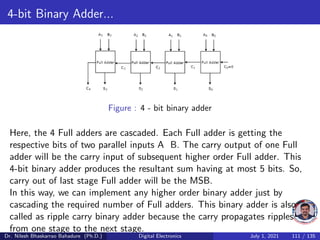
  • 110. 4-bit Binary Adder The 4-bit binary adder performs the addition of two 4-bit numbers. Let the 4-bit binary numbers, A=A3A2A1A0 and B=B3B2B1B0. We can implement 4-bit binary adder in one of the two following ways. 1 Use one Half adder for doing the addition of two Least significant bits and three Full adders for doing the addition of three higher significant bits. 2 Use four Full adders for uniformity. Since, initial carry Cin is zero, the Full adder which is used for adding the least significant bits becomes Half adder. For the time being, we considered second approach. The block diagram of 4-bit binary adder is shown in figure 51. Dr. Nilesh Bhaskarrao Bahadure (Ph.D.) Digital Electronics July 1, 2021 110 / 135
  • 111. 4-bit Binary Adder... Figure : 4 - bit binary adder Here, the 4 Full adders are cascaded. Each Full adder is getting the respective bits of two parallel inputs A B. The carry output of one Full adder will be the carry input of subsequent higher order Full adder. This 4-bit binary adder produces the resultant sum having at most 5 bits. So, carry out of last stage Full adder will be the MSB. In this way, we can implement any higher order binary adder just by cascading the required number of Full adders. This binary adder is also called as ripple carry binary adder because the carry propagates ripples from one stage to the next stage. Dr. Nilesh Bhaskarrao Bahadure (Ph.D.) Digital Electronics July 1, 2021 111 / 135
  • 112. Digital Subtractor Binary Subtraction can take many forms but the rules for subtraction are the same whichever process you use. As binary notation only has two digits, subtracting a ”0” from a ”0” or a ”1” leaves the result unchanged as 0-0 = 0 and 1-0 = 1. Subtracting a ”1” from a ”1” results in a ”0”, but subtracting a ”1” from a ”0” requires a borrow. In other words 0 1 requires a borrow. Dr. Nilesh Bhaskarrao Bahadure (Ph.D.) Digital Electronics July 1, 2021 112 / 135
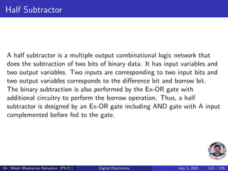
  • 113. Half Subtractor A half subtractor is a multiple output combinational logic network that does the subtraction of two bits of binary data. It has input variables and two output variables. Two inputs are corresponding to two input bits and two output variables corresponds to the difference bit and borrow bit. The binary subtraction is also performed by the Ex-OR gate with additional circuitry to perform the borrow operation. Thus, a half subtractor is designed by an Ex-OR gate including AND gate with A input complemented before fed to the gate. Dr. Nilesh Bhaskarrao Bahadure (Ph.D.) Digital Electronics July 1, 2021 113 / 135
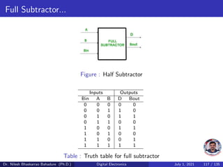
  • 114. Half Subtractor... Figure 52 shows the symbol, truth table and logic diagram of the hald subtractor circuit. Figure : Half Subtractor Dr. Nilesh Bhaskarrao Bahadure (Ph.D.) Digital Electronics July 1, 2021 114 / 135
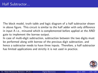
  • 115. Half Subtractor... The block model, truth table and logic diagram of a half subtractor shown in above figure. This circuit is similar to the half adder with only difference in input A i.e., minuend which is complemented before applied at the AND gate to implement the borrow output. In case of multi-digit subtraction, subtraction between the two digits must be performed along with borrow of the previous digit subtraction, and hence a subtractor needs to have three inputs. Therefore, a half subtractor has limited applications and strictly it is not used in practice. Dr. Nilesh Bhaskarrao Bahadure (Ph.D.) Digital Electronics July 1, 2021 115 / 135
  • 116. Full Subtractor A combinational logic circuit performs a subtraction between the two binary bits by considering borrow of the lower significant stage is called as the full subtractor. In this, subtraction of the two digits is performed by taking into consideration whether a 1 has already borrowed by the previous adjacent lower minuend bit or not. It has three input terminals in which two terminals corresponds to the two bits to be subtracted (minuend A and subtrahend B), and a borrow bit Bi corresponds to the borrow operation. There are two outputs, one corresponds to the difference D output and other borrow output Bo as shown in figure (Figure 53) along with truth table. Dr. Nilesh Bhaskarrao Bahadure (Ph.D.) Digital Electronics July 1, 2021 116 / 135
  • 117. Full Subtractor... Figure : Half Subtractor Inputs Outputs Bin A B D Bout 0 0 0 0 0 0 0 1 1 0 0 1 0 1 1 0 1 1 0 0 1 0 0 1 1 1 0 1 0 0 1 1 0 0 1 1 1 1 1 1 Table : Truth table for full subtractor Dr. Nilesh Bhaskarrao Bahadure (Ph.D.) Digital Electronics July 1, 2021 117 / 135
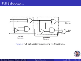
  • 118. Full Subtractor... Figure : Full Subtractor Circuit Dr. Nilesh Bhaskarrao Bahadure (Ph.D.) Digital Electronics July 1, 2021 118 / 135
  • 119. Full Subtractor... Figure : Full Subtractor Circuit using Half Subtractor Dr. Nilesh Bhaskarrao Bahadure (Ph.D.) Digital Electronics July 1, 2021 119 / 135
  • 120. 4-bit Binary Subtractor The 4-bit binary subtractor produces the subtraction of two 4-bit numbers. Let the 4bit binary numbers, A=A3A2A1A0 and B=B3B2B1B0. Internally, the operation of 4-bit Binary subtractor is similar to that of 4-bit Binary adder. If the normal bits of binary number A, complemented bits of binary number B and initial carry borrow, Cin as one are applied to 4-bit Binary adder, then it becomes 4-bit Binary subtractor. The block diagram of 4-bit binary subtractor is shown in figure 56. Figure : 4-bit Binary Subtractor using Full Adder Dr. Nilesh Bhaskarrao Bahadure (Ph.D.) Digital Electronics July 1, 2021 120 / 135
  • 121. 4-bit Binary Subtractor... This 4-bit binary subtractor produces an output, which is having at most 5 bits. If Binary number A is greater than Binary number B, then MSB of the output is zero and the remaining bits hold the magnitude of A-B. If Binary number A is less than Binary number B, then MSB of the output is one. So, take the 2s complement of output in order to get the magnitude of A-B. In this way, we can implement any higher order binary subtractor just by cascading the required number of Full adders with necessary modifications. Dr. Nilesh Bhaskarrao Bahadure (Ph.D.) Digital Electronics July 1, 2021 121 / 135
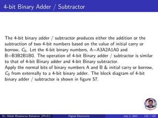
  • 122. 4-bit Binary Adder / Subtractor The 4-bit binary adder / subtractor produces either the addition or the subtraction of two 4-bit numbers based on the value of initial carry or borrow, C0. Let the 4-bit binary numbers, A=A3A2A1A0 and B=B3B2B1B0. The operation of 4-bit Binary adder / subtractor is similar to that of 4-bit Binary adder and 4-bit Binary subtractor. Apply the normal bits of binary numbers A and B & initial carry or borrow, C0 from externally to a 4-bit binary adder. The block diagram of 4-bit binary adder / subtractor is shown in figure 57. Dr. Nilesh Bhaskarrao Bahadure (Ph.D.) Digital Electronics July 1, 2021 122 / 135
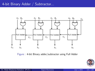
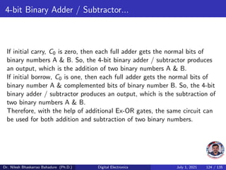
  • 123. 4-bit Binary Adder / Subtractor... Figure : 4-bit Binary adder/subtractor using Full Adder Dr. Nilesh Bhaskarrao Bahadure (Ph.D.) Digital Electronics July 1, 2021 123 / 135
  • 124. 4-bit Binary Adder / Subtractor... If initial carry, C0 is zero, then each full adder gets the normal bits of binary numbers A & B. So, the 4-bit binary adder / subtractor produces an output, which is the addition of two binary numbers A & B. If initial borrow, C0 is one, then each full adder gets the normal bits of binary number A & complemented bits of binary number B. So, the 4-bit binary adder / subtractor produces an output, which is the subtraction of two binary numbers A & B. Therefore, with the help of additional Ex-OR gates, the same circuit can be used for both addition and subtraction of two binary numbers. Dr. Nilesh Bhaskarrao Bahadure (Ph.D.) Digital Electronics July 1, 2021 124 / 135
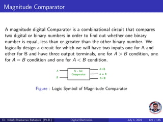
  • 125. Magnitude Comparator A magnitude digital Comparator is a combinational circuit that compares two digital or binary numbers in order to find out whether one binary number is equal, less than or greater than the other binary number. We logically design a circuit for which we will have two inputs one for A and other for B and have three output terminals, one for A > B condition, one for A = B condition and one for A < B condition. Figure : Logic Symbol of Magnitude Comparator Dr. Nilesh Bhaskarrao Bahadure (Ph.D.) Digital Electronics July 1, 2021 125 / 135
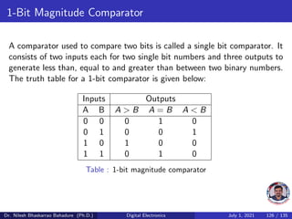
  • 126. 1-Bit Magnitude Comparator A comparator used to compare two bits is called a single bit comparator. It consists of two inputs each for two single bit numbers and three outputs to generate less than, equal to and greater than between two binary numbers. The truth table for a 1-bit comparator is given below: Inputs Outputs A B A > B A = B A < B 0 0 0 1 0 0 1 0 0 1 1 0 1 0 0 1 1 0 1 0 Table : 1-bit magnitude comparator Dr. Nilesh Bhaskarrao Bahadure (Ph.D.) Digital Electronics July 1, 2021 126 / 135
  • 127. 1-Bit Magnitude Comparator... From the above truth table logical expressions for each output can be expressed as follows: A > B : AB0 A < B : A0 B A = B : A0 B0 + AB Figure : 1-bit Digital Comparator Circuit Dr. Nilesh Bhaskarrao Bahadure (Ph.D.) Digital Electronics July 1, 2021 127 / 135
  • 128. Note A = B : A0 B0 + AB = AB0 + A0B (XNOR = XOR) Dr. Nilesh Bhaskarrao Bahadure (Ph.D.) Digital Electronics July 1, 2021 128 / 135
  • 129. 2-Bit Magnitude Comparator A comparator used to compare two binary numbers each of two bits is called a 2-bit Magnitude comparator. It consists of four inputs and three outputs to generate less than, equal to and greater than between two binary numbers. Figure : 2-bit Magnitude Comparator Dr. Nilesh Bhaskarrao Bahadure (Ph.D.) Digital Electronics July 1, 2021 129 / 135
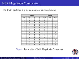
  • 130. 2-Bit Magnitude Comparator... The truth table for a 2-bit comparator is given below: Figure : Truth table of 2-bit Magnitude Comparator Dr. Nilesh Bhaskarrao Bahadure (Ph.D.) Digital Electronics July 1, 2021 130 / 135
  • 131. 2-Bit Magnitude Comparator... The k-map simplification for the above truth table is as follows. Figure : k-map simplification Dr. Nilesh Bhaskarrao Bahadure (Ph.D.) Digital Electronics July 1, 2021 131 / 135
  • 132. 2-Bit Magnitude Comparator... A > B : A1B10 + A0B10 B00 + A1A0B00 A = B : A10 A00 B10 B00 + A10 A0B10 B0 + A1A0B1B0 + A1A00 B1B00 : A10 B10 (A00 B00 + A0B0) + A1B1(A0B0 + A00 B00 ) : (A0B0 + A00 B00 )(A1B1 + A10 B10 ) : (A0Ex − NorB0)(A1Ex − NorB1) A < B : A10 B1 + A00 B1B0 + A10 A00 B0 Dr. Nilesh Bhaskarrao Bahadure (Ph.D.) Digital Electronics July 1, 2021 132 / 135
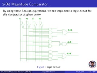
  • 133. 2-Bit Magnitude Comparator... By using these Boolean expressions, we can implement a logic circuit for this comparator as given below: Figure : logic circuit Dr. Nilesh Bhaskarrao Bahadure (Ph.D.) Digital Electronics July 1, 2021 133 / 135
  • 134. Dr. Nilesh Bhaskarrao Bahadure (Ph.D.) Digital Electronics July 1, 2021 134 / 135
  • 135. Thank you Please send your feedback at nbahadure@gmail.com For download and more information Click Here Dr. Nilesh Bhaskarrao Bahadure (Ph.D.) Digital Electronics July 1, 2021 135 / 135