SlideShare a Scribd company logo
TECHNOLOGICAL UNIVERSITY OF THE PHILIPPINES
AYALA BOULEVARD, ERMITA, MANILA
COLLEGE OF ENGINEERING
ASSIGNMET NO.3
Zener Diode, LED, and Seven Segment Display
Submitted by: DATE GIVEN: SEPTEMBER 14, 2016
Llorera, Jeshua B. DATE SUBMITTED: SEPTEMBER 21, 2016
BSME-4D
Submitted To:
ENGR. EDWIN C. ESPINAS
INSTRUCTOR RATING
ZENER DIODE
Applications:
Zener Diode as a voltage
In a DC circuit, Zener diode can be used as a voltage regulator or to provide voltage
reference. The main use of zener diode lies in the fact that the voltage across a Zener
diode remains constant for a larger change in current. This makes it possible to use a
Zener diode as a constant voltage device or a voltage regulator.
In any power supply circuit, a regulator is used to provide a constant output (load)
voltage irrespective of variation in input voltage or variation in load current. The
variation in input voltage is called line regulation, whereas the variation in load current is
called load regulation.
Zener Diode as voltage regulator
A simple circuit involving Zener diode as a regulator requires a resistor of low value
connected in series with the input voltage source. The low value is required so as to allow
the maximum flow of current through the diode, connected in parallel. However, the only
constraint being, the current through zener diode should not be less than minimum zener
diode current. Simply put, for a minimum input voltage and a maximum load current, the
Zener diode current should always be Izmin.
While designing a voltage regulator using zener diode, the latter is chosen with respect to
its maximum power rating. In other words, the maximum current through the device
should be:-
Imax = Power/Zener Voltage
Since the input voltage and the required output voltage is known, it is easier to choose a
zener diode with a voltage approximately equal to the load voltage, i.e. Vz ~=Vo.
The value of the series resistor is chosen to be
R = (Vin – Vz)/ (Izmin + IL), where IL = Load Voltage/Load resistance.
Note that for load voltages up to 8V, a single zener diode can be used. However for load
voltages beyond 8V, requiring Zener voltages of higher voltage value, it is advisable to
use a forward biased diode in series with the Zener diode. This is because the Zener diode
at higher voltage follows the avalanche breakdown principle, having a positive
temperature of coefficient.
Hence a negative temperature coefficient diode is used for compensation. Of course,
these days, practical temperature compensated Zener diodes are used.
Zener Diode as a voltage reference
Zener diode as voltage reference
In power supplies and many other circuits, Zener diode finds its application as a constant
voltage provider or a voltage reference. The only conditions are that the input voltage
should be greater than zener voltage and the series resistor should have a minimum value
such that the maximum current flows through the device.
Zener Diode as a voltage clamper
In a circuit involving AC input source, different from the normal PN diode clamping
circuit, a Zener diode can also be used. The diode can be used to limit the peak of the
output voltage to zener voltage at one side and to about 0V at other side of the sinusoidal
waveform.
zener diode as voltage clamper
In the above circuit, during positive half cycle, once the input voltage is such that the
zener diode is reverse biased, the output voltage is constant for a certain amount of time
till the voltage starts decreasing.
Now during the negative half cycle, the zener diode is in forward biased connection. As
the negative voltage increases till forward threshold voltage, the diode starts conducting
and the negative side of the output voltage is limited to the threshold voltage.
Note that to get an output voltage in positive range only, use two oppositely biased Zener
diodes in series.
Construction:
The Zener diode's operation depends on the heavy doping of its p-n junction. The
depletion region formed in the diode is very thin (<1 µm) and the electric field is
consequently very high (about 500 kV/m) even for a small reverse bias voltage of about
5 V, allowing electrons to tunnel from the valence band of the p-type material to the
conduction band of the n-type material.
At the atomic scale, this tunnelling corresponds to the transport of valence band electrons
into the empty conduction band states; as a result of the reduced barrier between these
bands and high electric fields that are induced due to the relatively high levels of doping
on both sides. The breakdown voltage can be controlled quite accurately in the doping
process. While tolerances within 0.07% are available, the most widely used tolerances are
5% and 10%. Breakdown voltage for commonly available Zener diodes can vary widely
from 1.2 volts to 200 volts.
For diodes that are lightly doped the breakdown is dominated by the avalanche effect
rather than the Zener effect. Consequently, the breakdown voltage is higher (over 5.6 V)
for these devices.
Characteristics:
The Zener Diode goes through a number of different regions or stages, of which are
explained below.
The right half side of the characteristics curve is the part in which the zener diode
receives forward voltage, which is the positive voltage across its anode to cathode
terminals. The diode in this region is in forward biased. During this period, the current is
small for a while until it spikes exponentially up once the voltage reaches a certain point,
called the threshold voltage.
The left half side of the characteristics curve is the more important part, when
considering zener diodes. This is the part in which the zener diode receives positive
voltage across its cathode to anode terminals. The diode in this region is in reverse
biased. At first, when receiving reverse voltage, the current is very small. There is only a
small current, called the leakage current, flowing through the diode. Once it hits the
breakdown voltage, the current drastically increases. This current is the called the
avalanche current, because it spikes so drastically up. The breakdown voltage point is
also important, not just because of the avalanche current, but more importantly because
once the voltage of the zener diode has reached this point, it remains constant at this
voltage, even though the current across it may increase largely. This makes the zener
diode useful in applications such as voltage regulation.
The zener diode has the important characteristic in that once the voltage across a zener
has reached this breakdown voltage, also called a zener diode's zener voltage, VZ, the
voltage that a zener drops across itself will not continue to increase. For example, if a
zener diode has a zener voltage of 5.1V, and the voltage feeding the diode is
approximately around 5.1V, the zener will drop the 5.1V across its terminals. Now if the
voltage supplying it continues to increase, to say 12V, the zener diode will maintain its
zener voltage, 5.1V, even though the voltage (and current) supplying it continues to
increase.
This is the single most important characteristic of a zener diode, which as stated before,
allows it it to act as a voltage regulator in a circuit. The voltage that is dropped across a
zener will not exceed its breakdown or zener voltage, even if the voltage or current in the
circuit increases, which is what the I-V characteristics curve above depicts.
LED
LED APPLICATION:
LEDs are utilized in many industries for many things. The applications of this efficient and
environmentally-friendly light source are endless, however, there are 5 main fields of application:
automotive use, backlight sources for consumer electronics, display screens for advertising,
electronic equipment, and generallighting.
Automotive:
Uses for the interior of automobiles include indicator lights on dashboard gauges, audio status
lights, security status lights and warning signals. Automobile exterior usage includes third brake
lights, the left and right rear lamps, turn signals, etc. Currently many European series vehicles
including Audi and BMW integrate high power LEDs.
Backlight Sources:
The mobile phone is the largest market of integration for SMD (surface mount diode) LEDs. An
estimated 400 million mobile phones are sold annually. One mobile phone takes two LED
backlight sources and six SMD LED key lights. As a result, mobile phones create a demand for
3.2 billion LEDs per year.
Display Screen:
The LED screen has become the new display medium for advertising and information. It is
commonly used in concert, arena and trade show venues. Its popularity has prompted the rapid
technological development of large-scale integrated circuits. Compared to plasma- and LCD-
based displays and traditional media such as neon lights, LED displays offer advantages such as
high brightness, dynamic visual display, high reliability, low energy consumption, long service
life, display content diversity, high durability, and low maintenance costs. LED display screens
have been widely adapted in various fields.
Electronic Equipment:
Due to attributes such as low power consumption, small size, and long life, LEDs have become
the preferred light source on various electronic equipment. Today, LEDs have been integrated as
warning lights and indicators on most electronics.
General Lighting:
LEDs are being used in advertising billboards, illumination of commercial building exteriors,
landmark buildings, bridges, roads, town centers and landscape lighting because of the numerous
advantages they offer. Their long life, rich color, and easily-controlled features with integrated
electronics offer a scalable lighting solution. As technology continues to bring rapid
improvements in luminous efficiency and as cost compression persists, applications expand
rapidly. Many airports, subways, Hotels, shopping centers,and individual homes feature LEDs
now. The integration of LED-based solutions into traffic lighting has been successfuland is also
growing rapidly.
LED Construction:
One of the methods used to construct LED is to deposit three semiconductor layers on the
substrate. The three semiconductor layers deposited on the substrate are n-type
semiconductor, p-type semiconductor and active region. Active region is present in
between the n-type and p-type semiconductor layers.
When LED is forward biased, free electrons from n-type semiconductor and holes from
p-type semiconductor are pushed towards the active region.
When free electrons from n-side and holes from p-side recombine with the opposite
charge carriers (free electrons with holes or holes with free electrons) in active region, an
invisible or visible light is emitted.
In LED, most of the charge carriers recombine at active region. Therefore, most of the
light is emitted by the active region. The active region is also called as depletion region.
LED characteristics:
Individual LEDs are low voltage devices. Single indicator LEDs require 2 to 4 volts of direct current, with
current in the range from 1 to 50 milliamperes. An illumination-grade LED containing a single
semiconducting element requires the same voltage, but operating currents are much higher, typically
several hundred milliamperes. A device containing multiple elements connected in series will require
higher voltage corresponding to the larger number of individual elements in the device.
LEDs require a specific electrical polarity Applying voltage in reverse polarity can destroy them.
Manufacturers provide specifications about the maximum reverse voltages acceptable for LED devices; 5
volts is a typical maximum rating.
There is a wide variety of different LEDs available on the market. The different LED characteristics
include colours light / radiation wavelength, light intensity,and a variety of other LED characteristics.
The different LED characteristics have been brought about by a variety of factors, in the manufacture of the
LED. The semiconductor make-up is a factor, but fabrication technology and encapsulation also play major
part of the determination of the LED characteristics.
LED colours
One of the major characteristics of an LED is its colour. Initially LED colours were very restricted. For the
first years only red LEDs were available.
However as semiconductor processes were improved and new research was undertaken to investigate new
materials for LEDs, different colours became available.
The diagram below shows some typical approximate curves for the voltages that may be expected for
different LED colours.
Typical (approximate) LED voltage curves
LED voltage drops
The voltage drop across an LED is different to that of a normal silicon LED. Typically the LED voltage
drop is between around 2 and 4 volts.
The actual LED voltage that appears across the two terminals is dependent mainly upon the type of LED in
question - the materials used.
As would be expected the LED voltage curve broadly follows that which would be expected for the
forward characteristic for a diode. However once the diode has turned on, the voltage is relatively flat for a
variety of forward current levels. This means that in some cases designers have used them as very rough
voltage stabilisers - zener diodes do not operate at voltages as low as LEDs. However their performance is
obviously nowhere near as good.
Seven segment display
SevenSegmentDisplayApplications:
The applications of seven segments are mostly in digital calculators, electronic meters, digital
clocks, odometers, digital clocks, clock radios, etc.
Today most of the 7 segment applications are using LCDs,because of low current consumption.
Seven Segment Display Construction:
The individual segments of a seven-segment display.A seven segment display, as its name
indicates, is composed of seven elements. Individually on or off, they can be combined to
produce simplified representations of the arabic numerals. Often the seven segments are arranged
in an oblique (slanted) arrangement, which aids readability. In most applications, the seven
segments are of nearly uniform shape and size (usually elongated hexagons, though trapezoids
and rectangles can also be used), though in the case of adding machines, the vertical segments are
longer and more oddly shaped at the ends in an effort to further enhance readability.
Each of the numbers 0, 6, 7 and 9 may be represented by two or more different glyphs on seven-
segment displays.
LED-based 7-segment display showing the 16 hex digits.The seven segments are arranged as a
rectangle of two vertical segments on each side with one horizontal segment on the top, middle,
and bottom. Additionally, the seventh segment bisects the rectangle horizontally. There are also
fourteen-segment displays and sixteen-segment displays (for full alphanumerics); however, these
have mostly been replaced by dot-matrix displays.
The segments of a 7-segment display are referred to by the letters A to G, as shown to the right,
where the optional DP decimal point (an "eighth segment") is used for the display of non-integer
numbers.
The animation to the left cycles through the common glyphs of the ten decimal numerals and the
six hexadecimal "letter digits" (A–F). It is an image sequence of a "LED" display, which is
described technology-wise in the following section. Notice the variation between uppercase and
lowercase letters for A–F; this is done to obtain a unique, unambiguous shape for each letter
(otherwise, a capital D would look identical to an 0 (or less likely O) and a capital B would look
identical to an 8).
Seven segments are,effectively, the fewest required to represent each of the ten Hindu-Arabic
numerals with a distinct and recognizable glyph.
Bloggers have experimented with six-segment and even five-segment displays with such novel
shapes as curves,angular blocks and serifs for segments; however, these often require
complicated and/or non-uniform shapes and sometimes create unrecognizable glyphs.
Seven Segment Display Characteristics:
There are two types of LED 7-segment displays: common cathode (CC) and common anode
(CA). The difference between the two displays is the common cathode has all the cathodes of the
7-segments connected directly together and the common anode has all the anodes of the 7-
segments connected together. Shown below is a common anode seven segment.
As shown above all the anode segments are connected together. When working with a CA seven
segment display, power must be applied externally to the the anode connection that is common to
all the segments. Then by applying a ground to a particular segment connection (a-g), the
appropriate segment will light up. An additional resistor must be added to the circuit to limit the
amount of current flowing thru each LED segment.
The above diagram shows the instance when power is applied to the CA connection and segments
b & c are grounded causing these two segments to light up. A typical pinout for a seven segment
common anode display is shown below.
A common cathode seven segment is different from a common anode segment in that the
cathodes of all the LEDs are connected together. For the use of this seven segment the common
cathode connection must be grounded and power must be applied to appropriate segment in order
to illuminate that segment.

More Related Content

PPTX
Semiconductor Diode: Introduction and Application
PDF
VI Characteristics of Diode
PPTX
Diode ,its types & its Application
DOCX
Types of Diodes
PPT
Special purpose diode
PPTX
Tunnel diode
PPTX
Zener Diode Presentation
PPTX
Types of Diodes Advantages and disadvantages, LE
Semiconductor Diode: Introduction and Application
VI Characteristics of Diode
Diode ,its types & its Application
Types of Diodes
Special purpose diode
Tunnel diode
Zener Diode Presentation
Types of Diodes Advantages and disadvantages, LE

What's hot (20)

PPT
Diodes
PDF
Diodes and rectifiers
PPT
Diode theory
PPT
PPTX
PPTX
Zener diode and its applications
PPT
PN JUNCTION
PDF
The Complete Diode Model
PPTX
Full sessional pack ii
PPTX
ZENER DIODE
PPTX
Zener diode and full wave rectifier or bridge connection
PPT
Pn junction diode class 12 investegatory project
PPT
Diode
PPT
Semiconductor diodes
PPT
Zenerdiodes
PPTX
Semiconductor diode
PPTX
Different semiconductor diodes.ppt
PDF
PPTX
Varactor, step recovery diodes and frequency multiplier
PPT
Halderman ch048 lecture
Diodes
Diodes and rectifiers
Diode theory
Zener diode and its applications
PN JUNCTION
The Complete Diode Model
Full sessional pack ii
ZENER DIODE
Zener diode and full wave rectifier or bridge connection
Pn junction diode class 12 investegatory project
Diode
Semiconductor diodes
Zenerdiodes
Semiconductor diode
Different semiconductor diodes.ppt
Varactor, step recovery diodes and frequency multiplier
Halderman ch048 lecture
Ad

Viewers also liked (13)

PPTX
PDF
portfolio2
PDF
0423_導入ゼミ_吉澤裕也「建物(法政付近)」
PPTX
Dyslexia: Time For Talent
PPTX
La entrevista
PDF
0423_導入ゼミ_福地和来「東京カテドラル聖マリア大聖堂」
PPT
Yoghurt and pears cake
PPTX
13 6 19_3期末報告
PPS
How Motivational Action Plans Influence Performance
DOCX
VAISAKH- Resume
PDF
Farming Unicorns: Building Startup & Investor Ecosystems (Madrid, June 2016)
PDF
Build Your Own Valley: Engineering Startup & Investor Ecosystems in Emerging ...
portfolio2
0423_導入ゼミ_吉澤裕也「建物(法政付近)」
Dyslexia: Time For Talent
La entrevista
0423_導入ゼミ_福地和来「東京カテドラル聖マリア大聖堂」
Yoghurt and pears cake
13 6 19_3期末報告
How Motivational Action Plans Influence Performance
VAISAKH- Resume
Farming Unicorns: Building Startup & Investor Ecosystems (Madrid, June 2016)
Build Your Own Valley: Engineering Startup & Investor Ecosystems in Emerging ...
Ad

Similar to Ece ass (20)

PPTX
Zener Diode and Light Emitting Diode (LED.pptx
PPTX
Bee Electronic microproject Roll No.41 to 44.pptx
PPTX
I-v charateristics of zener diode
PPTX
presentatio of electical engineer of topic on problem
PPTX
Zener Diode Introduction and working .pptx
PDF
Zener diode
PPTX
Zener Diode Full Presentation
PPT
anery-Whats Diode
DOCX
Physics Investigatory:To Study V-I Characteristics Of Zener Diode
PPTX
PPTX
Real&Special Diodeswhatdiodeareanduses.pptx
PPTX
SamikshaDeole1.pptx
PPT
Zener Diodes.ppt
PPTX
Special Purpose Diode AND THIRE APPLICATION ppt.pptx
PPT
Chapter 3 special_purpose_diodes Phy.ppt
DOCX
Informe 4
PPTX
Zener diode
PDF
Special Diodes zener, led, photodiode and varactors
PPTX
Zener diode
PPTX
Electronic Devices - Special Diodes - Unit 1.pptx
Zener Diode and Light Emitting Diode (LED.pptx
Bee Electronic microproject Roll No.41 to 44.pptx
I-v charateristics of zener diode
presentatio of electical engineer of topic on problem
Zener Diode Introduction and working .pptx
Zener diode
Zener Diode Full Presentation
anery-Whats Diode
Physics Investigatory:To Study V-I Characteristics Of Zener Diode
Real&Special Diodeswhatdiodeareanduses.pptx
SamikshaDeole1.pptx
Zener Diodes.ppt
Special Purpose Diode AND THIRE APPLICATION ppt.pptx
Chapter 3 special_purpose_diodes Phy.ppt
Informe 4
Zener diode
Special Diodes zener, led, photodiode and varactors
Zener diode
Electronic Devices - Special Diodes - Unit 1.pptx

Recently uploaded (20)

PPTX
bas. eng. economics group 4 presentation 1.pptx
PDF
Arduino robotics embedded978-1-4302-3184-4.pdf
DOCX
573137875-Attendance-Management-System-original
PDF
BMEC211 - INTRODUCTION TO MECHATRONICS-1.pdf
PPTX
web development for engineering and engineering
PPTX
Engineering Ethics, Safety and Environment [Autosaved] (1).pptx
PPTX
CH1 Production IntroductoryConcepts.pptx
PDF
Mohammad Mahdi Farshadian CV - Prospective PhD Student 2026
PPTX
Foundation to blockchain - A guide to Blockchain Tech
PPTX
UNIT-1 - COAL BASED THERMAL POWER PLANTS
PPTX
Sustainable Sites - Green Building Construction
PPTX
MCN 401 KTU-2019-PPE KITS-MODULE 2.pptx
PPTX
MET 305 2019 SCHEME MODULE 2 COMPLETE.pptx
PDF
Model Code of Practice - Construction Work - 21102022 .pdf
PDF
Well-logging-methods_new................
PPTX
OOP with Java - Java Introduction (Basics)
PPT
Mechanical Engineering MATERIALS Selection
DOCX
ASol_English-Language-Literature-Set-1-27-02-2023-converted.docx
PDF
SM_6th-Sem__Cse_Internet-of-Things.pdf IOT
PDF
Embodied AI: Ushering in the Next Era of Intelligent Systems
bas. eng. economics group 4 presentation 1.pptx
Arduino robotics embedded978-1-4302-3184-4.pdf
573137875-Attendance-Management-System-original
BMEC211 - INTRODUCTION TO MECHATRONICS-1.pdf
web development for engineering and engineering
Engineering Ethics, Safety and Environment [Autosaved] (1).pptx
CH1 Production IntroductoryConcepts.pptx
Mohammad Mahdi Farshadian CV - Prospective PhD Student 2026
Foundation to blockchain - A guide to Blockchain Tech
UNIT-1 - COAL BASED THERMAL POWER PLANTS
Sustainable Sites - Green Building Construction
MCN 401 KTU-2019-PPE KITS-MODULE 2.pptx
MET 305 2019 SCHEME MODULE 2 COMPLETE.pptx
Model Code of Practice - Construction Work - 21102022 .pdf
Well-logging-methods_new................
OOP with Java - Java Introduction (Basics)
Mechanical Engineering MATERIALS Selection
ASol_English-Language-Literature-Set-1-27-02-2023-converted.docx
SM_6th-Sem__Cse_Internet-of-Things.pdf IOT
Embodied AI: Ushering in the Next Era of Intelligent Systems

Ece ass

  • 1. TECHNOLOGICAL UNIVERSITY OF THE PHILIPPINES AYALA BOULEVARD, ERMITA, MANILA COLLEGE OF ENGINEERING ASSIGNMET NO.3 Zener Diode, LED, and Seven Segment Display Submitted by: DATE GIVEN: SEPTEMBER 14, 2016 Llorera, Jeshua B. DATE SUBMITTED: SEPTEMBER 21, 2016 BSME-4D Submitted To: ENGR. EDWIN C. ESPINAS INSTRUCTOR RATING
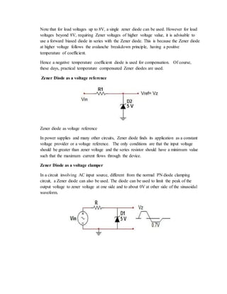
  • 2. ZENER DIODE Applications: Zener Diode as a voltage In a DC circuit, Zener diode can be used as a voltage regulator or to provide voltage reference. The main use of zener diode lies in the fact that the voltage across a Zener diode remains constant for a larger change in current. This makes it possible to use a Zener diode as a constant voltage device or a voltage regulator. In any power supply circuit, a regulator is used to provide a constant output (load) voltage irrespective of variation in input voltage or variation in load current. The variation in input voltage is called line regulation, whereas the variation in load current is called load regulation. Zener Diode as voltage regulator A simple circuit involving Zener diode as a regulator requires a resistor of low value connected in series with the input voltage source. The low value is required so as to allow the maximum flow of current through the diode, connected in parallel. However, the only constraint being, the current through zener diode should not be less than minimum zener diode current. Simply put, for a minimum input voltage and a maximum load current, the Zener diode current should always be Izmin. While designing a voltage regulator using zener diode, the latter is chosen with respect to its maximum power rating. In other words, the maximum current through the device should be:- Imax = Power/Zener Voltage Since the input voltage and the required output voltage is known, it is easier to choose a zener diode with a voltage approximately equal to the load voltage, i.e. Vz ~=Vo. The value of the series resistor is chosen to be R = (Vin – Vz)/ (Izmin + IL), where IL = Load Voltage/Load resistance.
  • 3. Note that for load voltages up to 8V, a single zener diode can be used. However for load voltages beyond 8V, requiring Zener voltages of higher voltage value, it is advisable to use a forward biased diode in series with the Zener diode. This is because the Zener diode at higher voltage follows the avalanche breakdown principle, having a positive temperature of coefficient. Hence a negative temperature coefficient diode is used for compensation. Of course, these days, practical temperature compensated Zener diodes are used. Zener Diode as a voltage reference Zener diode as voltage reference In power supplies and many other circuits, Zener diode finds its application as a constant voltage provider or a voltage reference. The only conditions are that the input voltage should be greater than zener voltage and the series resistor should have a minimum value such that the maximum current flows through the device. Zener Diode as a voltage clamper In a circuit involving AC input source, different from the normal PN diode clamping circuit, a Zener diode can also be used. The diode can be used to limit the peak of the output voltage to zener voltage at one side and to about 0V at other side of the sinusoidal waveform.
  • 4. zener diode as voltage clamper In the above circuit, during positive half cycle, once the input voltage is such that the zener diode is reverse biased, the output voltage is constant for a certain amount of time till the voltage starts decreasing. Now during the negative half cycle, the zener diode is in forward biased connection. As the negative voltage increases till forward threshold voltage, the diode starts conducting and the negative side of the output voltage is limited to the threshold voltage. Note that to get an output voltage in positive range only, use two oppositely biased Zener diodes in series. Construction: The Zener diode's operation depends on the heavy doping of its p-n junction. The depletion region formed in the diode is very thin (<1 µm) and the electric field is consequently very high (about 500 kV/m) even for a small reverse bias voltage of about 5 V, allowing electrons to tunnel from the valence band of the p-type material to the conduction band of the n-type material. At the atomic scale, this tunnelling corresponds to the transport of valence band electrons into the empty conduction band states; as a result of the reduced barrier between these bands and high electric fields that are induced due to the relatively high levels of doping on both sides. The breakdown voltage can be controlled quite accurately in the doping process. While tolerances within 0.07% are available, the most widely used tolerances are 5% and 10%. Breakdown voltage for commonly available Zener diodes can vary widely from 1.2 volts to 200 volts. For diodes that are lightly doped the breakdown is dominated by the avalanche effect rather than the Zener effect. Consequently, the breakdown voltage is higher (over 5.6 V) for these devices.
  • 5. Characteristics: The Zener Diode goes through a number of different regions or stages, of which are explained below. The right half side of the characteristics curve is the part in which the zener diode receives forward voltage, which is the positive voltage across its anode to cathode terminals. The diode in this region is in forward biased. During this period, the current is small for a while until it spikes exponentially up once the voltage reaches a certain point, called the threshold voltage. The left half side of the characteristics curve is the more important part, when considering zener diodes. This is the part in which the zener diode receives positive voltage across its cathode to anode terminals. The diode in this region is in reverse biased. At first, when receiving reverse voltage, the current is very small. There is only a small current, called the leakage current, flowing through the diode. Once it hits the breakdown voltage, the current drastically increases. This current is the called the avalanche current, because it spikes so drastically up. The breakdown voltage point is also important, not just because of the avalanche current, but more importantly because once the voltage of the zener diode has reached this point, it remains constant at this voltage, even though the current across it may increase largely. This makes the zener diode useful in applications such as voltage regulation. The zener diode has the important characteristic in that once the voltage across a zener has reached this breakdown voltage, also called a zener diode's zener voltage, VZ, the voltage that a zener drops across itself will not continue to increase. For example, if a zener diode has a zener voltage of 5.1V, and the voltage feeding the diode is approximately around 5.1V, the zener will drop the 5.1V across its terminals. Now if the voltage supplying it continues to increase, to say 12V, the zener diode will maintain its zener voltage, 5.1V, even though the voltage (and current) supplying it continues to increase. This is the single most important characteristic of a zener diode, which as stated before, allows it it to act as a voltage regulator in a circuit. The voltage that is dropped across a zener will not exceed its breakdown or zener voltage, even if the voltage or current in the circuit increases, which is what the I-V characteristics curve above depicts.
  • 6. LED LED APPLICATION: LEDs are utilized in many industries for many things. The applications of this efficient and environmentally-friendly light source are endless, however, there are 5 main fields of application: automotive use, backlight sources for consumer electronics, display screens for advertising, electronic equipment, and generallighting. Automotive: Uses for the interior of automobiles include indicator lights on dashboard gauges, audio status lights, security status lights and warning signals. Automobile exterior usage includes third brake lights, the left and right rear lamps, turn signals, etc. Currently many European series vehicles including Audi and BMW integrate high power LEDs. Backlight Sources: The mobile phone is the largest market of integration for SMD (surface mount diode) LEDs. An estimated 400 million mobile phones are sold annually. One mobile phone takes two LED backlight sources and six SMD LED key lights. As a result, mobile phones create a demand for 3.2 billion LEDs per year. Display Screen: The LED screen has become the new display medium for advertising and information. It is commonly used in concert, arena and trade show venues. Its popularity has prompted the rapid technological development of large-scale integrated circuits. Compared to plasma- and LCD- based displays and traditional media such as neon lights, LED displays offer advantages such as high brightness, dynamic visual display, high reliability, low energy consumption, long service life, display content diversity, high durability, and low maintenance costs. LED display screens have been widely adapted in various fields. Electronic Equipment: Due to attributes such as low power consumption, small size, and long life, LEDs have become the preferred light source on various electronic equipment. Today, LEDs have been integrated as warning lights and indicators on most electronics. General Lighting: LEDs are being used in advertising billboards, illumination of commercial building exteriors, landmark buildings, bridges, roads, town centers and landscape lighting because of the numerous advantages they offer. Their long life, rich color, and easily-controlled features with integrated electronics offer a scalable lighting solution. As technology continues to bring rapid improvements in luminous efficiency and as cost compression persists, applications expand rapidly. Many airports, subways, Hotels, shopping centers,and individual homes feature LEDs now. The integration of LED-based solutions into traffic lighting has been successfuland is also growing rapidly.
  • 7. LED Construction: One of the methods used to construct LED is to deposit three semiconductor layers on the substrate. The three semiconductor layers deposited on the substrate are n-type semiconductor, p-type semiconductor and active region. Active region is present in between the n-type and p-type semiconductor layers. When LED is forward biased, free electrons from n-type semiconductor and holes from p-type semiconductor are pushed towards the active region. When free electrons from n-side and holes from p-side recombine with the opposite charge carriers (free electrons with holes or holes with free electrons) in active region, an invisible or visible light is emitted. In LED, most of the charge carriers recombine at active region. Therefore, most of the light is emitted by the active region. The active region is also called as depletion region. LED characteristics: Individual LEDs are low voltage devices. Single indicator LEDs require 2 to 4 volts of direct current, with current in the range from 1 to 50 milliamperes. An illumination-grade LED containing a single semiconducting element requires the same voltage, but operating currents are much higher, typically several hundred milliamperes. A device containing multiple elements connected in series will require higher voltage corresponding to the larger number of individual elements in the device.
  • 8. LEDs require a specific electrical polarity Applying voltage in reverse polarity can destroy them. Manufacturers provide specifications about the maximum reverse voltages acceptable for LED devices; 5 volts is a typical maximum rating. There is a wide variety of different LEDs available on the market. The different LED characteristics include colours light / radiation wavelength, light intensity,and a variety of other LED characteristics. The different LED characteristics have been brought about by a variety of factors, in the manufacture of the LED. The semiconductor make-up is a factor, but fabrication technology and encapsulation also play major part of the determination of the LED characteristics. LED colours One of the major characteristics of an LED is its colour. Initially LED colours were very restricted. For the first years only red LEDs were available. However as semiconductor processes were improved and new research was undertaken to investigate new materials for LEDs, different colours became available. The diagram below shows some typical approximate curves for the voltages that may be expected for different LED colours. Typical (approximate) LED voltage curves LED voltage drops The voltage drop across an LED is different to that of a normal silicon LED. Typically the LED voltage drop is between around 2 and 4 volts. The actual LED voltage that appears across the two terminals is dependent mainly upon the type of LED in question - the materials used. As would be expected the LED voltage curve broadly follows that which would be expected for the forward characteristic for a diode. However once the diode has turned on, the voltage is relatively flat for a variety of forward current levels. This means that in some cases designers have used them as very rough voltage stabilisers - zener diodes do not operate at voltages as low as LEDs. However their performance is obviously nowhere near as good.
  • 9. Seven segment display SevenSegmentDisplayApplications: The applications of seven segments are mostly in digital calculators, electronic meters, digital clocks, odometers, digital clocks, clock radios, etc. Today most of the 7 segment applications are using LCDs,because of low current consumption. Seven Segment Display Construction: The individual segments of a seven-segment display.A seven segment display, as its name indicates, is composed of seven elements. Individually on or off, they can be combined to produce simplified representations of the arabic numerals. Often the seven segments are arranged in an oblique (slanted) arrangement, which aids readability. In most applications, the seven segments are of nearly uniform shape and size (usually elongated hexagons, though trapezoids and rectangles can also be used), though in the case of adding machines, the vertical segments are longer and more oddly shaped at the ends in an effort to further enhance readability. Each of the numbers 0, 6, 7 and 9 may be represented by two or more different glyphs on seven- segment displays. LED-based 7-segment display showing the 16 hex digits.The seven segments are arranged as a rectangle of two vertical segments on each side with one horizontal segment on the top, middle, and bottom. Additionally, the seventh segment bisects the rectangle horizontally. There are also fourteen-segment displays and sixteen-segment displays (for full alphanumerics); however, these have mostly been replaced by dot-matrix displays. The segments of a 7-segment display are referred to by the letters A to G, as shown to the right, where the optional DP decimal point (an "eighth segment") is used for the display of non-integer numbers. The animation to the left cycles through the common glyphs of the ten decimal numerals and the six hexadecimal "letter digits" (A–F). It is an image sequence of a "LED" display, which is described technology-wise in the following section. Notice the variation between uppercase and lowercase letters for A–F; this is done to obtain a unique, unambiguous shape for each letter (otherwise, a capital D would look identical to an 0 (or less likely O) and a capital B would look identical to an 8). Seven segments are,effectively, the fewest required to represent each of the ten Hindu-Arabic numerals with a distinct and recognizable glyph. Bloggers have experimented with six-segment and even five-segment displays with such novel shapes as curves,angular blocks and serifs for segments; however, these often require complicated and/or non-uniform shapes and sometimes create unrecognizable glyphs.
  • 10. Seven Segment Display Characteristics: There are two types of LED 7-segment displays: common cathode (CC) and common anode (CA). The difference between the two displays is the common cathode has all the cathodes of the 7-segments connected directly together and the common anode has all the anodes of the 7- segments connected together. Shown below is a common anode seven segment. As shown above all the anode segments are connected together. When working with a CA seven segment display, power must be applied externally to the the anode connection that is common to all the segments. Then by applying a ground to a particular segment connection (a-g), the appropriate segment will light up. An additional resistor must be added to the circuit to limit the amount of current flowing thru each LED segment. The above diagram shows the instance when power is applied to the CA connection and segments b & c are grounded causing these two segments to light up. A typical pinout for a seven segment common anode display is shown below.
  • 11. A common cathode seven segment is different from a common anode segment in that the cathodes of all the LEDs are connected together. For the use of this seven segment the common cathode connection must be grounded and power must be applied to appropriate segment in order to illuminate that segment.