

![What is Power Factor?
The goal of any power factor correction circuit is to emulate a resistance
The absorbed current must be sinusoidal and in phase with the input voltage
in
v t
in
i t
in
i
in
v
in
in in in in
v t
p t i t v t v t
R
,
0
1
70 W
line
T
in avg in
line
P p t dt
T
, , , 85 823 70 VA
in app in rms in rms
P V I m
line
T
active power [W]
PF 1
apparent power [V A]
in
v t
in
i t
in
i
in
v
70 W
70 W
,
0
1
70 W
line
T
in avg in
line
P p t dt
T
, , , 85 1.46 124 VA
in app in rms in rms
P V I
active power [W]
PF 0.56
apparent power [V A]
](https://image.slidesharecdn.com/introductiontopfc-240605095654-fbc310d8/85/Introduction-to-Power-factor-correction-in-industries-3-320.jpg)

![Explaining Power Factor with Beer
A low power factor will force the circulation of a higher rms current
Electric wires can overheat and utility companies push for power factor correction
A glass of beer with an excessive foam can help appreciate the issue
Apparent
power S
supplied by
the utility
Useless
circulating
power
Average power
contributing
the work
2 2
S P jQ
P
P Q
PF
2
1
1
PF
Q P
VAR 33% W
Q P
https://www.iberdrola.es/en/homeowners-associations/information/reactive-power
If PF < 0.95
[VA] [W] [VAR]](https://image.slidesharecdn.com/introductiontopfc-240605095654-fbc310d8/85/Introduction-to-Power-factor-correction-in-industries-5-320.jpg)


Introduction to Power factor correction in industries
- 1. Christophe Basso Business Development Manager IEEE Senior Member A Tutorial Introduction to Power Factor Correction August 2022 – Rev 0.36
- 2. Agenda Notions of Power Factor Power Factor Correction Structures Processing the Power Loop Compensation of a PFC Solutions from Future Suppliers
- 3. What is Power Factor? The goal of any power factor correction circuit is to emulate a resistance The absorbed current must be sinusoidal and in phase with the input voltage in v t in i t in i in v in in in in in v t p t i t v t v t R , 0 1 70 W line T in avg in line P p t dt T , , , 85 823 70 VA in app in rms in rms P V I m line T active power [W] PF 1 apparent power [V A] in v t in i t in i in v 70 W 70 W , 0 1 70 W line T in avg in line P p t dt T , , , 85 1.46 124 VA in app in rms in rms P V I active power [W] PF 0.56 apparent power [V A]
- 4. What is the Impact of a Low PF? Assume a 250-W load absorbed by an equipment from a 110-V 15-A ac outlet With a PF of 0.56, the current is 250/110/0.56 4 A rms You can safely connect a maximum of 3 devices (15/4 = 3.75) 250 W – PF = 0.56 110 V – 15 A Pmax = 1.65 kVA x 3 You can safely connect 6 workstations 250 W – PF = 0.99 110 V – 15 A Pmax = 1.65 kVA x 6 PFC Add a front-end power factor correction stage to bring PF close to unity Iin,rms = 2.3 A Iin,rms = 4 A
- 5. Explaining Power Factor with Beer A low power factor will force the circulation of a higher rms current Electric wires can overheat and utility companies push for power factor correction A glass of beer with an excessive foam can help appreciate the issue Apparent power S supplied by the utility Useless circulating power Average power contributing the work 2 2 S P jQ P P Q PF 2 1 1 PF Q P VAR 33% W Q P https://www.iberdrola.es/en/homeowners-associations/information/reactive-power If PF < 0.95 [VA] [W] [VAR]
- 6. Power Factor and Distortion Power factor depends on two parameters: 1, PF cos rms rms d I I k k Total rms current Fundamental rms current kd represents the distortion factor k designates the displacement angle i t v t i t v t i t v t i t v t kd < 1, k < 1 kd < 1, k = 1 kd = 1, k < 1 kd = 1, k = 1 0 20 40 60 80 100 0.7 0.8 0.9 1 THD (%) PF For a displacement angle k of 1: 1 PF THD 1 100 THD = 30%, PF = 0.958 THD = 10% PF = 0.995 THD = 5% PF = 0.999 Check harmonics limits according to IEC1000-3-2
- 7. Equipment Compliance The standard EN61000-3-2 defines the class of equipment and associated limits Class C Lighting equipment? PC/monitor TV? Class B Portable tool? Motor equipment? 3-phase equipment? Class A Class D no no yes yes yes Enter no Pin > 75 W Pin > 75 W Class D limits no J. Turchi, D. Dalal, Power Factor Correction: from Basics to Optimization, Technical Seminar, APEC 2014 yes yes no
- 8. The Need for Storage The goal of a PFC front-end converter is to emulate a resistive load The power of a single-phase ac source feeding a resistance involves a squared sinewave in v t in i t in in in p t v t i t 150 W in P 0 300 (W) 150 W in p t 10 20 30 40 (ms) Power excess Power shortage Active power factor stores and release energy 50 Hz F 100 Hz F Store energy Release energy in v t out v t 400 V 420 V 380 V Output voltage ripple is twice the input frequency Output capacitor in p t
- 9. Agenda Notions of Power Factor Power Factor Correction Structures Processing the Power Loop Compensation of a PFC Solutions from Future Suppliers
- 10. Passive Power Factor Correction Capacitor refueling in a full-bridge rectifier is confined at the sinewave peak A very narrow spike is generated, rich of numerous harmonics Spreading the current across the sinewave smooths the current signature in v t in i t L1 = 0 H L1 = 34 mH Pout = 100 W Iin,rms = 1.8 A without L Iin,rms = 1.2 A with L = 34 mH Choke is bulky, heavy and induces mechanical stress Reduces rms current but marginal results harmonic-wise choke
- 11. Active Power Factor Correction An active PFC forces a sinusoidal current absorption in phase with the voltage A boost converter is traditionally employed for this operation L i t in i t d i t SW i t DRV L i t in i t out v t 400 V Cbulk RL rec v t The rectified input voltage sets the inductor current envelope The inductor current is adjusted to match power demand 100- or 120-Hz ripple
- 12. Conduction Mode – BCM or CrM Inductor current reduces to 0 A before a new cycle starts in borderline conduction mode Well suited for power levels up to 300 W or higher with interleaved version Near-zero-voltage switching in some conditions Discontinuous operation reduces trr-related power dissipation on the diode L i t L i t Ip 2 p L I i t Ip Averaged inductor current Variable-frequency switching makes light-load operation less efficient Internal frequency clamp or foldback is generally implemented to reduce losses Large circulating currents inducing conduction (rms) and core losses (IL) 0 A ton toff CrM: CRitical Conduction Mode
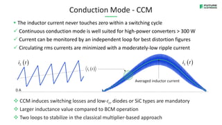
- 13. Conduction Mode - CCM The inductor current never touches zero within a switching cycle Continuous conduction mode is well suited for high-power converters > 300 W Current can be monitored by an independent loop for best distortion figures Circulating rms currents are minimized with a moderately-low ripple current L i t Averaged inductor current L i t 0 A CCM induces switching losses and low-trr diodes or SiC types are mandatory Larger inductance value compared to BCM operation Two loops to stabilize in the classical multiplier-based approach L i t
- 14. Single-Stage Converters It is possible to combine a PFC stage with an isolated flyback converter This single-stage approach is well adapted to power levels up to 100-150 W The components count is reduced It provides galvanic isolation to the downstream load Large output capacitance for the storing process Fairly-distorted input current barely passes PF specifications Slow-loop operation makes it well suited for lighting systems in i t in v t
- 15. Bridgeless PFC The bridge hampers overall efficiency with two permanently-conducting diodes , 2 d f d avg P V I , , 2 2 out F avg ac LL P I V P = 300 W = 100% Vac,LL = 90 V rms The bridgeless PFC ensures one diode conduction via the MOSFET body Pd 5 W Eff. loss 1.7% High-frequency operation Low-frequency operation Only one diode is conducting in low frequency The MOSFETs share a common drive signal without caring about line polarity Poor common-mode noise signature D. Mitchell, Ac-Dc Converter having Improved Power Factor, U.S. Patent 4,412,277, Oct. 25, 1983 Positive Negative
- 16. DRV L2 DRV D2 D1 Q1 D6 D7 C1 L1 Q2 Variation of the Bridgeless PFC The original scheme suffers from a poor common-mode EMI signature A variation around this circuit was proposed by Ivo Barbi in 1999 Two PFC in parallel driven by the same pattern – easy to drive with one controller Conventional structure automatically activated depending on the line polarity Turn-on snubber A. F. de Souza and I. Barbi, High power factor rectifier with reduced conduction and commutation losses, 21st International Telecommunications Energy Conference. INTELEC '99 (Cat. No.99CH37007), 1999 B. J. Turchi, A High-Efficiency 300-W Bridgeless PFC Stage, AND8481/D, onsemi, 2014 Active pos. cycle Active neg. cycle Low-frequency diodes vin(t)
- 17. The Totem-Pole PFC The two high-frequency switches are connected in a half-bridge configuration Two diodes in the slow leg route the low-frequency portion of the input current D1 S2 S1 V1 + C1 D4 D2 D3 R1 L1 Fast leg High frequency Slow leg 10 ms 0 V + - out V The fast-leg transistors alternatively perform as power switch and catch diode D2 and D1 must be fast diodes with no recovery loss: SiC or GaN transistors are perfect for this function D3 and D4 can be controlled-switches for improved efficiency Common-mode noise improved compared to bridgeless PFC
- 18. The Need to Detect the Input Line Polarity Each fast-leg transistor alternatively plays the role of the switch and the diode The switching element needs instruction on the input line polarity Manage line polarity
- 19. Dedicated Controllers for TPPFC onsemi has introduced two low-voltage controllers operating in BCM and CCM NCP1680 can implement a pre-converter up to 300 W One single inductor with auxiliary winding ensures ZVS operation Line management with a pair of resistive dividers Two external drivers dedicated to fast and slow legs: NCP51820 and NCP51530
- 20. Efficiency Performance of the BCM TPPFC The TPPFC efficiency is excellent compared with a classical approach A gain of 1.8% is brought by the all-synchronous approach at 90-V rms input voltage 300-W PFC demonstration board NCP1680 265 V rms 230 V rms 115 V rms 90 V rms Efficiency approaches 99% at 230 V rms and full power
- 21. TPPFC High-Power Operations Continuous conduction mode is selected for high-power PFC pre-converters The NCP1681 includes a multi-mode engine operating in CCM, BCM and DCM Mode change is inhibited for high-power applications and the part keeps CCM Slow leg Fast leg Add aux. winding for multi-mode
- 22. Multi-Mode Operations The downstream converter may operate with different load profiles, low to high current CCM is optimized for high power but BCM and DCM bring better efficiency in lighter loads NCP1681 embarks a multi-mode engine smoothly transitioning across all these modes TSW TSW DCM valley switching 1st valley BCM High-power CCM The part internally compares operating timings with thresholds to determine the mode The mode is kept during an entire half cycle Reference timing
- 23. Managing Current Transformers Fast-leg switches play the main power switch or the rectifier role in a TPPFC Current flow in the leg depends on the input line polarity and needs specific action Current transformers secondaries are alternatively shorted depending on line polarity L i t Inductor current downslope FDS8935 Inductor current upslope
- 24. A Reliable Controller with Fault Management The controller permanently monitors operating variables for maximum protection Some minor faults involve a quick recovery while heavier issues start a 500-ms timer UVP or under-voltage protection monitors the FB pin and checks for a bias before delivering pulses BUV or bulk under-voltage checks that the output voltage is above 80% of its nominal value Soft OVP is active when a benign overshoot is detected like a load release Hard OVP can be seen as more severe fault in case of stronger overshoot or loop failure
- 25. NCP1681 Evaluation Board A 500-W demonstration board operated in multi-mode By-pass diodes CT blanking Optional in-rush limiter Slow-leg To upper fast-leg
- 26. The Control Section The NCP1681 senses the polarity via two resistive networks The slow-leg requires a bootstrapped driver but of lesser speed than for GaNs Polarity indicator for CT short Zero crossing detection for inductor current downslope Feedback connection for regulation and BUV Input mains polarity detection Slow-leg control signal To GaNs To SJ MOSFETs One option with isolated gate driver NCP51561 and discrete GaNs (GS66508B) One option with one NCP51561 and two NCP58921 Vcc OVP and OTP
- 27. NCP51561 Half-Bridge Driver Isolated drivers are preferred for the fast leg considering switching speed and noise Differential voltage up to 1.5 kV between channels 5-ns delay matching and pulse distortion Common Mode Transient Immunity grater than 200 V/ns
- 28. NCP58921 Integrated GaN Driver Integrated GaN and driver simplifies PCB layout and reduces BOM cost NCP58921 NCP51560 CT blanking GaN + driver GaN + driver
- 29. Efficiency Charts with Multi-Mode Engine The multi-mode engines clearly shows its positive effects in light-load conditions
- 30. Operating Waveforms The part excels in distortion performance which keeps below 5% at full load Vin = 115 V rms – THD = 4.2% Vin = 230 V rms – THD = 2.7% iin(t) iin(t) vCS(t) vCS(t) vM(t) vM(t) vSW(t) vSW(t)
- 31. Agenda Notions of Power Factor Power Factor Correction Structures Processing the Power Loop Compensation of a PFC Solutions from Future Suppliers
- 32. Constant On-Time Control Voltage-mode control offers the easiest implementation for BCM PFCs Start with the inductor instantaneous current waveform: L i t 2 peak L I i t 0 A ton toff peak I , 2 L peak in in in in i t p t v t i t v t , in L peak on v t i t t t L 2 2 in in on v t p t t t L 2 in in on v t i t t t L in in in in in ac v t v t i t P R V The power sets the on-time value in relationship with the rms input voltage 2 2 in on ac LP t V 18 µs on t SW f t L i t 2 sin 2 ac on in V t i t t L constant On-time is constant Frequency is variable Resistive input
- 33. Modulating the On-Time A capacitor is charged by a constant-current source The error voltage modulates the toggling threshold and adjusts ton COMP FB Q Ct Verr verr(t) vPWM(t) Pout increases Pout decreases vCt(t) Q A maximum on-time clamp limits the power This clamp can be adjusted based on the line level Modulation around the 0-V input improves distortion ton Vref t t
- 34. Voltage-Mode Operation Constant on-time can be implemented in voltage-mode control No need to sense the input voltage! DRV VOUT R6 {Rupper} Frequency Frequency IN D Q QN RST SET U2 R11 {Rlower} G1 {gm} S2 Vrect C7 100n DRV FB C5 470n R4 250m IC=1 R10 R13 30m DRV R14 30m VB IL R2 22k IC=1 R3 R5 {R2} S1 Duty Cycle Duty ratio IN C8 47p IC=0 P1 TX1 S1 IC=1 R31 D2 mr756 + C4 1u IC=0 + C10 22p IC=1 C3 {C1} DRV Ct R8 100m FB Iin U1 D1 mr756 275u I1 R1 1K C2 {C2} IC=1 R9 + C13 200u IC=0 5m L3 + Ct 1n IC=0 U3 I2 {Vref1} V4 Q QN R S U35 V6 V2 100m V3 10m V1 5m L4 On-time modulator Demagnetization detection Compensation Bypass diode L i t in i t sw f t FB v t out v t rect v t Zero-crossing distortion
- 35. Peak-Current-Mode Operation R12 1K R13 30m rect R1 220m R11 {Rlower} IC=1 R10 R14 30m S1 D Q QN RST SET U2 Q QN R S U35 R7 1K R8 100m V3 10m IC=1 R31 R6 {Rupper} P1 TX1 S1 V6 R2 22k R5 {R2} V2 100m {Vref1} V4 IC=1 R3 V1 U3 Multiplier IN1 IN2 OUT U4 U1 R4 250m IC=1 R9 DRV C1 100p + C10 22p IC=1 + C13 200u IC=0 C2 {C2} + C4 1u IC=0 C5 470n C8 47p IC=0 D1 mr756 rect DRV FB D2 mr756 E1 600m C3 {C1} rect C7 100n 7.5m E2 IL 5m L3 5m L4 Vout VFB G1 {gm} Iin The inductor peak current follows the rectified voltage for a sinusoidal envelope o A multiplier is needed to sense the input voltage: increased power consumption L i t in i t FB v t out v t rect v t Multiplier Compensation Demagnetization detection Bypass diode
- 36. A Multiplier in the Chip The inductor current is scaled by the rectified voltage and follows the envelope A small offset is added to the multiplier and effectively reduces Fsw near 0 V S R Q in v t div k mul a b k ref V Compensator err V div in k v t c v t i R Inductor reset b a Multiplier m k off k i p R i t + - reset c V in v t a b 0.0417 off k 0.65 mult k mult k FB V 1.9 V Offset limits Fsw excursion Input sensing
- 37. Harmonic Distortion Enhancer The front-end capacitor holds some residual voltage near zero crossing A THD enhancer typically forces a higher on-time at low input voltage L6564H data-sheet Front-end capacitor does not discharge to 0 V
- 38. R4 1K R2 L1 260u R14 R6 R5 U3 C3 C1 D6 Rsense D3 C8 Q1 R13 D1 R12 R1 C7 D7 D2 U1 R3 U2 C2 330u Average Mode Current The inductor current is shaped by a dedicated high-bandwidth loop Error between the inductor current and setpoint is minimized for best distortion in k v t in err k v t V Current loop err V 2.5 V sense v t 100 V rms 1 kW in out V P in i t THD 2.3% 100 V rms THD 2.9% 230 V rms in in V V Multiplier needed!
- 39. A High-Speed Current Loop It is important to ensure the fast and precise tracking of the current envelope The current loop must exhibit a wide bandwidth, e.g. 10 kHz typically OUT 99.4967 -503.267m BO 399.998 B3 V=V(AMPI)/2.5 > 0.99 ? 0.99 : V(AMPI)/2.5 Rs L1 {L} Iin Iout PWMVMCCM U1 AC 1 V5 D1 mr756 R13 2.8k C7 10n R11 15m AMPI C2 300u R12 2.2k R14 2.2k C8 220p U2 99.3457 E2 {KBO} {Vrms} V1 Rsense {Rsense} R4 100m From control circuitry
- 40. Predictive Power Factor Most of the PFC circuits do sense the input voltage to build the control law Predictive timing generates PWM control without high-voltage sensing c a p in V out V L C R SW D Switching cell + - 0 L v t c in v t V 1 c out out off v t V D V D in out off V V D L v t The input current is the inductor current in L i t i t in L i t i t in out off in L v t V D i t i t Sam Ben-Yaakov and Ilya Zeltser, PWM Converters with Resistive Input, IEEE Transactions on Industrial Electronics, vol. 45, Issue: 3, June 1998) Input resistance e off L out R D i t V e R Set the control law to program Doff(t) Depends on power Regulated output e off in out R D t i t V in e off out e v t R d t V R Average values Instantaneous variables
- 41. No Input Voltage Sensing By modulating the off-time duration across the input line, resistive input is ensured The input current is sensed via a shunt and averaged through a low-pass filter The error voltage adjusts the capacitor charging current and hence off-time duration ch m e I g V ch m e ch ch I g V v t t t C C LP filter Experimental embodiment L s v t i t R v v m e off L s ch g V T i t R C toggling v L s ch off e m sw i t R C D t V g T Method and Apparatus for Regulating the Input Impedance of PWM Converters, S. Ben-Yaakov, M. Hadar, Green Power Technologies, US 6,307,361B1
- 42. Simulation Example The application circuit is simple and requires a specific off-time modulator A dedicated amplifier shapes the negative input current via a shunt Vrect R12 {Rload} R1 IC=1 R2 {Rlower} 2u I1 + C13 330u IC=372 C5 470n R4 250m Rect FB G1 10u IC=1 R3 5m L4 C7 100n R11 80m C1 100p R13 30m R14 30m Clock D1 mr756 {gm} G2 Ct VA IL Clock 5m L3 Ct + C2 {C2} IC=0 Ct VFB Vdrain VOUT C8 150p Q VB D2 mr756 ISW C3 {C1} + C4 1u IC=0 C6 220p Iin L1 260u U1 S1 R9 2.2k V5 AC 1 V1 S2 R7 2.2k V2 {Vref} V4 R6 {Rupper} OPSIMP U2 R5 {R2} R8 10m Sense resistor modulator 0 0.01 0.02 0.03 0.04 0.05 0 0.1 0.2 0.3 0.4 200 100 0 100 200 doff t ( ) vin t ( ) t in v t off D t The average off-time is modulated along the input sinewave Part of my 80+ ready-made templates available here
- 43. Simulation Results The input current waveform is perfectly sinusoidal and undistorted in i t Off-time On-time L i t Distortion data: Pout = 1 kW Vin = 100 V rms THD = 3% Vin = 230 V rms THD = 6% Vin = 100 V rms, Pout = 1 kW Regulated output voltage
- 44. Single-Stage Converter It is possible to combine a PFC function with a flyback converter Very popular in lighting applications where bandwidth is naturally low Operates in quasi-resonant mode Power factor is usually greater than 0.9 Constant on-time voltage-mode operation Typical operating waveforms – 120 V rms ZCD v t LED i t rect v t err v t
- 45. Agenda Notions of Power Factor Power Factor Correction Structures Processing the Power Loop Compensation of a PFC Solutions from Future Suppliers
- 46. A PFC is usually a boost converter operated in different conduction modes: Continuous Conduction Mode or CCM: high-power system, usually > 300 W Boundary/Borderline Conduction Mode or BCM: small to moderate power < 300 W Many derived structures like interleaved or totem-pole for higher power levels The PFC controller implements a control law: how to force a sinusoidal input current? In BCM converters, it is usually a constant on-time control, voltage- or current-mode In CCM, there are usually proprietary control laws optimizing distortion and efficiency The Need for Stability Regardless of the implementation, loop analysis is important to guaranty a stable and reliable operation MC33262 o Capacitor stress o OVP can be triggered o Poor stabilization time out v t
- 47. Modeling a Power Factor Correction Stage Several ways exist to model switching converters State-space averaging (SSA), PWM switch model, 1st-order approximation etc. A PFC is a slow system in essence with crossover frequency below 10 Hz 1st-order approximation averages power without considering switching mechanism load R in out P V out V err V Control VM or CM C r bulk C VM or CM CCM or BCM bulk C load R L If the load is a regulated switching converter, the incremental resistance is negative Simplified model in P Current source
- 48. A General Formula to Express the Output Power A generic PFC control law obeys the following formula: , , m in rms control in avg n out K V V P V m characterizes the input-voltage feed-forward n is 1 in general for predictive-sensing stages K is a constant which depends on the modulator, L, Rsense etc. J. Turchi, D. Dalal, Power Factor Correction: from Basics to Optimization, Technical Seminar, APEC 2014 This is a large-signal expression which needs to be linearized The corresponding model does not predict high-frequency phenomenon like RHPZ Perfect for low-frequency approach of a naturally-slow PFC stage Works for any type of operation, CCM, CrM/BCM, fixed or variable frequency etc. L i t CCM, fixed frequency L i t CrM, variable frequency 0 A 0 A
- 49. Example with CrM Power Factor Correction The power transmitted by a power stage operated in CrM obeys the formula: 2 , 2 ac in avg PWM err V P G V L constant on-time voltage-mode control GPWM represents the modulator small-signal gain L is the boost inductor value 100% efficiency 2 2 ac out PWM err out V I G V LV in out P P Run partial differentiation to obtain small-signal coefficients: 0 2 2 ˆ ˆ 0 ˆ ˆ ˆ 2 2 err out ac PWM err ac PWM err out out err out out err out v v V G V V G V i v v V L V V L V Nonlinear expression! C. Basso, Transfer Functions of Switching Converters, Faraday Press 2021 NCP1608 NCP1622 L6562 L6564 MP44019 MP44018
- 50. 0.01 0.1 1 10 100 40 20 0 20 40 80 60 40 20 0 20 log HLL i 2 fk arg HLL i 2 fk 180 fk Modeling a Power Factor Correction Stage From the small-signal equation, build the complete simplified model load R out V s C r bulk C load R 2 2 ac PWM err out V G V s L V 0 0 1 1 1 1 z p p s H s H H s s ESR contribution high frequency only 2 0 4 ac load PWM out V R G H L V 2 p load bulk R C stimulus response Assume the following specifications: 144 W 380 V 250 µH 200 1kΩ in out bulk load P V L C µF R 0 78 38 dB 1.6 Hz p H Plot power stage (LL) H f H f Dc gain varies with Vin squared 90 V rms in V (dB) (°)
- 51. Compensation Strategy for the PFC Without specific treatment, dc gain changes with line input squared For ratio of 2.3 between 265 V and 90 V rms input, gain changes by 2.942 9 Select a crossover fc = 50 Hz at a 265-V input to keep at least 8-10 Hz at lowest line 0 2 26.6 1 c c p H H f f f 50 Hz 1 tan 88 c c p f H f f Go for a type 2 Bring a 1/26.6 or 28.5-dB attenuation at 50 Hz For a 70° phase margin, boost the phase by: One pole and one zero to boost the phase by 68° fp = 260 Hz fz = 9.6 Hz 70 88 90 68 boost gain excess 0 1 1 z p s G s G s Type 2 compensator 50 Hz
- 52. Check Compensated Response A type 2 compensator is needed 0.01 0.1 1 10 100 1 10 3 1 10 4 50 0 50 100 0 100 arg fk 0.01 0.1 1 10 100 1 10 3 1 10 4 50 0 50 100 0 100 arg fk Check crossover and phase margin at the input line extremes 2 C 1 C 2 R err V s 1 R lower R 1 R lower R out V s out V s m g ref V ref V 2 C 1 C 2 R err V s Operational Transconductance Amplifier (OTA) Operational Amplifier (op-amp) T f T f T f T f (dB) (dB) (°) (°) m c f m c f T s H s G s 8.5 Hz 50 c m f 50 Hz 70 c m f Low line, 90 V rms High line, 265 V rms HV output HV output
- 53. Simulate the Converter after Compensation SIMPLIS® is well suited for simulating power factor correction stages The program can plot the ac response from a switching circuit and simulates fast Error amplifier section On-time modulator ZCD winding Templates can be freely downloaded from https://cbasso.pagesperso-orange.fr/Spice.htm
- 54. Check Transient Response is Acceptable IN i t rec v t out i t out v t L i t 400 mA 600 mA The output current is stepped from 400 to 600 mA at the lowest 90-V rms input voltage 90 V rms in V
- 55. Transient Response at High Line IN i t rec v t out i t out v t L i t In high-line conditions, the PFC is stable but given the higher crossover, distortion suffers 400 mA 600 mA 265 V rms in V
- 56. Compensating a CCM PFC We take the example of a 1-kW PFC operated in continuous conduction mode An averaged model is used to extract the control-to-output transfer function The predictive controller is the NCP1654 from Predictive scheme of NCP1654
- 57. Closing the Loop The control-to-output transfer function is obtained with an averaged SPICE model Some in-line behavioral equations describe the controller’s internals Works in ac and transient analyzes .param Vrms=230 .param Vout=400 .param Pout=1.3k .param L=54u .param RBOL=82.5k .param RBOU=6.6Meg .param ROCP=3.8k .param Vp=2.5 .param Rsense=30m .param Ib=100u .param Rupper={(Vout-2.5)/Ib} .param Rlower={2.5/Ib} .param fc=20 .param Gfc=36.7 .param ps=-60 .param pm=60 .param gm=200u .param boost={PM-PS-90} .param G={10^(-Gfc/20)} .param k={tan((boost/2+45)*pi/180)} .param fp={fc*k} .param fz={fc/k} .param a={sqrt((fc^2/fp^2)+1)} .param b={sqrt((fz^2/fc^2)+1)} .param R2={(a/b)*(fp*G)*(Rlower+Rupper) +/((fp-fz)*Rlower*gm)} .param C1={1/(2*pi*R2*fz)} .param C2={(Rlower*gm/(2*pi*fp*G* +(Rlower+Rupper)))(b/a)} PWM switch model Control law Automatic computation Off-time modulation
- 58. The Power Stage Response The control-to-output transfer function is the starting point for compensation Infer a compensation strategy by reading information from magnitude and phase H f H f Vin = 100 V rms Vin = 230 V rms Crossover cannot be too high otherwise ripple may pollute the control voltage If too high then ripple will bring distortion and produce third harmonic Too low brings an unacceptable slow transient response Without feedforward the crossover may theoretically move with a factor of 9 in high- and low-line conditions NCP1654 feedforward limits the change in crossover frequency Power stage response Select fc in high-line conditions to obtain 5-10 Hz at low line fc,HL = 20 Hz J. Turchi, D. Dalal, Power Factor Correction: from Basics to Optimization, Technical Seminar, APEC 2014 20 Hz 36.7 dB H 20 Hz 57 H
- 59. Check Loop Gain The dc input voltage in an ac analysis is the rms voltage of the source Enter 100 V dc and 230 V dc for respective low- and high-line simulations T f T f Vin = 100 V rms Vin = 230 V rms fc,HL = 20 Hz fc,HL = 9 Hz PM low line = 78° PM high line = 62° G f G f Type 2 compensator Boost = 30° Vrms = 230 Vout = 400 Pout = 1.3k L = 54u RBOL = 82.5k RBOU = 6.6Meg ROCP = 3.8k Vp = 2.5 Rsense = 30m Ib = 100u Rupper = 3.975Meg Rlower = 25k fc = 20 Gfc = 36.7 ps = -60 pm = 60 gm = 200u boost = 30 G = 14.621771745m k = 1.73205080757 fp = 34.6410161514 fz = 11.5470053838 a = 1.15470053838 b = 1.15470053838 R2 = 17.546126093k C1 = 785.54219388n C2 = 392.77109694n Computed values: Compensator
- 60. Transient Response Performance The large-signal average model lends itself well to a transient simulation The input current at low line shows a good harmonic distortion figure of 4.2% in i t THDLL =4.23% THDHL =6.33% in i t out v t LL HL The output current is stepped from 300 W to 1.3 kW with a 1- A/µs slope The transient response is stable at low and high line out i t
- 61. Internal Digital Compensation The NCP1680 embarks an internal type 2 compensator A low-pass filter then follows to reduce the ripple contribution Mid-band gain is adjusted based on the input line value Type 2 compensator – analogue version Digital implementation 0 13.6 dB 1.44 Hz 68 Hz z p G Adjusted with line 0 1 1 z err out p V s s G s G s V s HV divider 1 R lower R out V s m g ref V 2 C 1 C 2 R err V s HV output
- 62. A Low-Pass Filter Reduces Feedback Ripple A low-pass filter is inserted in series with the compensator The digital implementation of this filter brings efficient output ripple rejection The sampling frequency is adjusted depending on the line frequency 2 2 1 1 N D s s Q G s s s Q 0.5 1 y n u n u n -45 0 45 100m 1 10 100 1k 2 4 6 8 20 40 60 200 600 -100 -80 -60 -40 -20 (dB) (°) LP G f LP G f Sampling frequency is 4Fline It sets a notch at twice the line frequency
- 63. SIMetrix Compensated Simulation The digital filter is simulated with delay lines and fed by a Laplace expression This is the digital low-pass filter sampled at 4 x Fline ba_z^-1 U5 AC 1 V1 ba_z^-1 U4 500m E7 -1 E8 {a2} E5 ARB5 V(N1)-V(N2) IN OUT =OUT/IN IN OUT =OUT/IN IN OUT =OUT/IN R2 25k {a1} E4 E1 1 ba_z^-1 U1 {b2} E3 ba_z^-1_2 In Out U2 n1 n2 OUT ARB2 V(N1)+V(N2) ARB4 V(N1)+V(N2)-V(N3) C1 1p R1 3.975Meg LAP1 H0/(k1+s/wpfc) ba_z^-1 U3 n1 n2 OUT ARB1 V(N1)+V(N2) E2 {b1} IN OUT =OUT/IN {a0} E6 Transfer function of the power stage Resistive divider gain Type 2 compensator Moving average low-pass filter Compensated loop gain
- 64. Typical Results for a 300-W Board The 300-W TPPFC features a constant crossover frequency regardless of input line T f T f Crossover frequency is almost unchanged Vin = 100 V rms Vin = 230 V rms m High line Low line
- 65. Agenda Notions of Power Factor Power Factor Correction Structures Processing the Power Loop Compensation of a PFC Solutions from Future Suppliers
- 66. Power Factor Controller Selection The selection of a PFC controller depends on various parameters: Constant on-time in BCM for low power, up to 200-300 W Want higher power in BCM: go for interleaved PFC Average mode control and CCM for high power, up to several kW Need for optimized efficiency? Go for multi-mode operation Need for the best efficiency? Go for a totem-pole PFC For compact design, go for a combo chip combining a PFC and a switching controller TEA2017: PFC and LLC FAN6921BMR: PFC and QR flyback IDP2308: PFC and LLC STCMB1: PFC and LLC HR1213: PFC and LLC PFC LLC
- 67. PFC Controllers from Part- Number Structure Operating Frequency Control Mode Operating Mode HV pin Package MP44018A Boost Variable VM BCM SO-8 MP44019 Boost Variable VM BCM SO-8 MP44010 Boost Variable VM BCM SO-8 HR1213 Combo LLC Variable Fixed CM CCM MM SO-20 HR1210 Combo LLC Variable Fixed CM CCM MM SO-20 HR1211 Combo LLC Variable Fixed VM CCM MM SO-16 https://www.monolithicpower.com/en/products/ac-dc/pfc-llc-controllers/pfc-llc-combo-controller.html
- 68. PFC Controllers from Part- Number Structure Operating Frequency Control Mode Operating Mode HV pin Package NCP1623 Boost Variable VM BCM TSOP-6 NCL2801 Boost Variable VM BCM SO-8 NCP1654 Boost Fixed CM CCM SO-8 NCP1680 Totem-pole Variable VM BCM SO-16 NCP1681 Totem-pole Variable Fixed CM CCM MM SO-20N FAN6921 Combo QR Variable VM BCM SO-16 NCP1937 Combo QR Variable VM BCM NCP1618 Boost Variable Fixed CM CCM MM SOIC-9 NCP1632 Interleaved Variable VM BCM SO-20 https://www.onsemi.com/products/power-management/ac-dc-power-conversion/power-factor-controllers
- 69. PFC Controllers from Part- Number Structure Operating Frequency Control Mode Operating Mode HV pin Package TEA19162HT Boost Variable VM BCM SO-8 TEA19162T Boost Variable VM BCM SO-8 TEA2017AAT Combo LLC Variable Fixed CM CCM MM SO-16 TEA2016AAT Combo LLC Variable Fixed CM CCM MM SO-16 https://www.nxp.com/products/power-management/ac-dc-solutions/ac-dc-controllers-with-integrated-pfc:MC_49476 The two standalone PFCs can be teamed up with LLC controller TEA19161T
- 70. PFC Controllers from Part- Number Structure Operating Frequency Control Mode Operating Mode HV pin Package ICE2PCS01/G Boost Adjustable CM CCM DIP/SO-8 ICE3PCS01G Boost Adjustable CM CCM SO-14 ICE3PCS03G Boost Adjustable CM CCM SO-8 ICE3PCS05/G Boost Adjustable CM CCM DIP/SO-8 IRS2505LPBF Boost Variable VM BCM SOT23-5 https://www.infineon.com/cms/en/product/power/ac-dc-power-conversion/ac-dc-pwm-pfc-controller/pfc-ccm-continuous-conduction-mode-ics/ ICE3PCS03G and ICE3PCS01G include an internal digital compensation
- 71. PFC Controllers from Part- Number Structure Operating Frequency Control Mode Operating Mode HV pin Package L6562A Boost Variable VM BCM DIP/SO-8 L6563S Boost Variable CM BCM SO-14 L6564 Boost Variable CM BCM SSOP-10 L6564H Boost Variable CM BCM SO-14 L4984D Boost Nearly Fixed CM FOT SSOP10 STCMB1 Combo LLC Variable Fixed VM BCM SO-20W https://www.st.com/en/power-management/pfc-controllers.html#
- 72. Conclusion Nonlinear loads force the unnecessary circulation of reactive power Reactive power flows in the grid and heats up distribution wires Mains rectification brings a poor power factor and distorts the current Power factor correction forces the absorption of a sinusoidal current It reduces the circulating reactive power and reduces the rms current The boost converter is a popular structure and can operate in: Borderline conduction mode up to 200-300 W Continuous conduction mode for high output levels beyond 1 kW Multi-mode combine best of both worlds for optimized efficiency The totem-pole PFC becomes popular owing to wide-bandgap components A PFC is a closed-loop system: pay attention to the stability