SlideShare a Scribd company logo
MOUSAM CHOUDHURY
Amity Institute of Nanotechnology
Amity University, Noida .
SCANNING
ELECTRON
MICROSCOPY
ELECTRON MICROSCOPY
- A BASIC MORPHOLOGICAL
STUDY EQUIPMENT FOR
POLYMER COMPOSITES AND
NANOCOMPOSITES
Electron microscope divided into the
following Basic components :-
1- Illumination system.
2- Imaging system.
3- Specimen stage.
4- Vacuum pump system.
5- Image recording system.
x-rays
composition
backscattered e's
microstructure
secondary e's
microstructure
elastically scattered e's
crystallographic structure
inelastically scattered e's
composition
transmitted e's
microstructure
SIGNALS IN ELECTRON MICROSCOPY
TYPES OF ELECTRON
MICROSCOPY FOR POLYMER
COMPOSITES
• SCANNING ELECTRON MICROSCOPE (SEM)
• TRANSMISSION ELECTRON MICROSCOPE (TEM)
SCANNING
ELECTRON
MICROSCOPE
SEM - Scanning Electron Microscopy
• tiny electron beam scanned across surface of specimen
• backscattered or secondary electrons detected
• signal output to synchronized display
WORKING OF SEM: SCANNING ELECTRON MICROSCOPE
ELECTRON GUN
ELECTRON EMITTER
Effects of increasing voltage in
electron gun:
•Resolution increased ( decreased)
•Penetration increases
•Specimen charging increases
(insulators)
•Specimen damage increases
•Image contrast decreases  = h/(2melectronqVo + q2Vo2/c2))1/2
VOLTAGE IN ELECTRON GUN:
FIELD EMISSION ELECTRON SOURCE:
High electric field at very sharp tip causes electrons to "tunnel"
maybe
FIELD EMISSION ELECTRON SOURCE:
ELECTRIC FIELD
High electric field at very sharp tip causes electrons to "tunnel"
cool tip ——> smaller E in beam
improved coherence
many electrons from small tip ——> finer
probe size, higher current densities (100X >)
problems - high vacuum
Electrons focused by Lorentz force from electromagnetic field
F = qv x B
effectively same as optical lenses
Lenses are ring-shaped
• coils generate magnetic field
• electrons pass thru hollow center
• lens focal length is continuously variable
• apertures control, limit beam
LENSES
Conducting -
• little or no preparation
• attach to mounting stub for
insertion into SEM instrument
• may need to provide
Conductive path with Ag paint
Non-conducting (E.g., Polymers and Plastics)-
usually coat with conductive very thin layer (Au, C, Cr)
SPECIMEN
Can examine
• fracture surfaces
• electronic devices
• fibers
• coatings
• particles
etc.
TYPES OF SPECIMENS (SOLID/ PARTICLE/ etc)
•Actually one at a time is
preferred
•However, four to five can be
placed on the stub
•The Specimen Holder can
be tilted, translated
•Specimen size limited by
size of sample chamber i.e.
the area of the stub
No. of Samples
THAT IS HOW AN IMAGE IS FORMED AND CALLED A MICROGRAPH
TYPES OF ELECTRONS FROM SPECIMEN
What comes from specimen?
Backscattered electrons
Secondary electrons
Fluorescent X-rays
high energy
compositional contrast
low energy
topographic contrastcomposition - EDS
Brightness of regions in image increases as
atomic number increases
(less penetration gives more backscattered
electrons)
BSEs
SEs
E/Eo
1
Main Electrons accounted for
a Micrograph, coming out
from specimen
• Backscattered electrons
• Secondary electrons
ELECTRON ENERGY DISTRIBUTION
Electron Energy up to 30-50 keV
annular around incident beam
repel secondary electrons with
— biased mesh
images are more sensitive to
•chemical composition (electron yield depends
on atomic number)
•line of sight necessary
BACKSCATTERED ELECTRON DETECTOR - SOLID STATE DETECTOR
SECONDARY ELECTRON DETECTOR - SCINTILLATION DETECTOR
+ bias mesh needed in front of
detector to attract low energy
electrons
line of sight unnecessary
INTERACTION VOLUME
Backscattered electrons
come from whole volume
(high energy)
Secondary electrons come
from neck only (low energy)
Fracture Surface in iron
SECONDARY
ELECTRONS
BACKSCATTERED
ELECTRONS
CHOOSE CORRECT DETECTOR- TOPOGRAPHY EXAMPLE
Comes from any kind of interaction with electron beam
 Topography
 Composition
o Elements
o Phases
 Grain (crystal) orientation
 Charging affects contrast
TYPES OF STUDY USING SEM
MAGNIFICATION – DETERMINED BY DISTANCE
RESOLUTION – DETERMINED BY PROBE SIZE
RESOLUTION – PROBE DIAMETER & PROBE SIZE
d = depth of field
 = required spatial resolution
a = convergence angle

d
region of image in focus
tana 
0.5
0.5d


d
For small angles, tana = a
d 

a
Can control depth of field (d) with convergence angle (a)
DEPTH OF FIELD
DEPTH OF FIELD
WD
Rap
tana 
Rap
WD
Thank you

More Related Content

PPTX
Scanning Electron Microscopy (SEM) lecture
PPTX
Scanning Electron Microscope
PPT
Transmission Electron Microscope
PPTX
Scanning electon microscope. Dr. GAURAV SALUNKHE
PPTX
Presentation on SEM (Scanning Electron Microscope)
PPTX
Scanning Electron Microscope
PPT
2018 HM-scanning electron microscope
PPTX
Scanning electron microscope (sem)
Scanning Electron Microscopy (SEM) lecture
Scanning Electron Microscope
Transmission Electron Microscope
Scanning electon microscope. Dr. GAURAV SALUNKHE
Presentation on SEM (Scanning Electron Microscope)
Scanning Electron Microscope
2018 HM-scanning electron microscope
Scanning electron microscope (sem)

What's hot (20)

PPTX
Scanning Electron Microscope (SEM)
PPTX
Scanning Electron Microscopy - SEM
PPTX
ELECTRON MICROSCOPY (TEM & SEM)
PPTX
Scanning Electron microscopy
PDF
Transmission electron microscope
PPTX
Electron microscope - SEM and TEM
PPTX
Scanning electron microscopy mubbu
PPTX
X ray photoelecton spectroscopy
PPTX
Scanning electron microscopy
PPTX
Transmission Electron Microscopy
PDF
SEM,TEM & AFM
PPTX
auger electron spectroscopy (AES)
PPTX
Scanning electron microscope
PPT
SEM- scanning electron microscope
PPTX
Transmission Electron Microscope
PPT
SEM and TEM
PDF
Scanning Electron Microscopy (SEM)
PPTX
Scanning electron microscopy
PPTX
Scanning electron microscope
Scanning Electron Microscope (SEM)
Scanning Electron Microscopy - SEM
ELECTRON MICROSCOPY (TEM & SEM)
Scanning Electron microscopy
Transmission electron microscope
Electron microscope - SEM and TEM
Scanning electron microscopy mubbu
X ray photoelecton spectroscopy
Scanning electron microscopy
Transmission Electron Microscopy
SEM,TEM & AFM
auger electron spectroscopy (AES)
Scanning electron microscope
SEM- scanning electron microscope
Transmission Electron Microscope
SEM and TEM
Scanning Electron Microscopy (SEM)
Scanning electron microscopy
Scanning electron microscope
Ad

Viewers also liked (6)

PPTX
Scanning electron microscope
PPTX
Electron Microscopy - Scanning electron microscope, Transmission Electron Mic...
PPTX
Scanning electron microscope
PPTX
Chaitrali jadhav:- scanning electron microscope
PPTX
Sem n tem
PPTX
Sem and tem
Scanning electron microscope
Electron Microscopy - Scanning electron microscope, Transmission Electron Mic...
Scanning electron microscope
Chaitrali jadhav:- scanning electron microscope
Sem n tem
Sem and tem
Ad

Similar to WORKING OF SEM: SCANNING ELECTRON MICROSCOPE (20)

PPT
Scanning electron microscopy
PPTX
scanning electron microscope (SEM)
PPTX
Electron Microscope Shanthakumar
PPTX
Scanning electron microscope
PPTX
Scanning electron microscopy
PPT
overview on scanning electron microscope
PPTX
Sem mahfooz
PPTX
Sem mahfooz
PPTX
electron microscopy
PPTX
Scanning Electron Microscopy
PPTX
Scanning Electron Microscope (SEM)
PPTX
PPTX
Dielectric surface imaging using scanning electron microsope
PPTX
Practical skills in scanning electron microscope
PPTX
Presentation forensic micoscopy SEM microscope.pptx
PPTX
Electron microscope
PPTX
Lec 3; Microscopy ALI.pptx
PPTX
Scanning electron microscopy
scanning electron microscope (SEM)
Electron Microscope Shanthakumar
Scanning electron microscope
Scanning electron microscopy
overview on scanning electron microscope
Sem mahfooz
Sem mahfooz
electron microscopy
Scanning Electron Microscopy
Scanning Electron Microscope (SEM)
Dielectric surface imaging using scanning electron microsope
Practical skills in scanning electron microscope
Presentation forensic micoscopy SEM microscope.pptx
Electron microscope
Lec 3; Microscopy ALI.pptx
Scanning electron microscopy

More from Mousam Choudhury (6)

PPTX
ECOSYSTEM & ENVIRONMENT WITH PLASTICS AN
PPTX
NATURAL RESOURCES Environment and Plastics
PPT
PLASTIC PROCESSING AIDS AND ADDITIVES IN AEAS OF POLYMER AND PETROCHEMICALS
POTX
TEMPLATE_MS-PPT_1.potx
PPTX
4.6.1 plastics testing.pptx
PPT
Plastic product manufacturing ideas for business 01072020.ppt
ECOSYSTEM & ENVIRONMENT WITH PLASTICS AN
NATURAL RESOURCES Environment and Plastics
PLASTIC PROCESSING AIDS AND ADDITIVES IN AEAS OF POLYMER AND PETROCHEMICALS
TEMPLATE_MS-PPT_1.potx
4.6.1 plastics testing.pptx
Plastic product manufacturing ideas for business 01072020.ppt

Recently uploaded (20)

PDF
Placing the Near-Earth Object Impact Probability in Context
PPTX
famous lake in india and its disturibution and importance
PDF
Mastering Bioreactors and Media Sterilization: A Complete Guide to Sterile Fe...
PDF
ELS_Q1_Module-11_Formation-of-Rock-Layers_v2.pdf
PPTX
Cell Membrane: Structure, Composition & Functions
PPTX
Introduction to Fisheries Biotechnology_Lesson 1.pptx
PPTX
BIOMOLECULES PPT........................
PPTX
Taita Taveta Laboratory Technician Workshop Presentation.pptx
PPTX
DRUG THERAPY FOR SHOCK gjjjgfhhhhh.pptx.
PDF
AlphaEarth Foundations and the Satellite Embedding dataset
PDF
IFIT3 RNA-binding activity primores influenza A viruz infection and translati...
PDF
CAPERS-LRD-z9:AGas-enshroudedLittleRedDotHostingaBroad-lineActive GalacticNuc...
PDF
HPLC-PPT.docx high performance liquid chromatography
PPTX
Derivatives of integument scales, beaks, horns,.pptx
PPTX
2. Earth - The Living Planet Module 2ELS
PDF
SEHH2274 Organic Chemistry Notes 1 Structure and Bonding.pdf
PPT
The World of Physical Science, • Labs: Safety Simulation, Measurement Practice
PPTX
TOTAL hIP ARTHROPLASTY Presentation.pptx
PPTX
cpcsea ppt.pptxssssssssssssssjjdjdndndddd
PDF
Sciences of Europe No 170 (2025)
Placing the Near-Earth Object Impact Probability in Context
famous lake in india and its disturibution and importance
Mastering Bioreactors and Media Sterilization: A Complete Guide to Sterile Fe...
ELS_Q1_Module-11_Formation-of-Rock-Layers_v2.pdf
Cell Membrane: Structure, Composition & Functions
Introduction to Fisheries Biotechnology_Lesson 1.pptx
BIOMOLECULES PPT........................
Taita Taveta Laboratory Technician Workshop Presentation.pptx
DRUG THERAPY FOR SHOCK gjjjgfhhhhh.pptx.
AlphaEarth Foundations and the Satellite Embedding dataset
IFIT3 RNA-binding activity primores influenza A viruz infection and translati...
CAPERS-LRD-z9:AGas-enshroudedLittleRedDotHostingaBroad-lineActive GalacticNuc...
HPLC-PPT.docx high performance liquid chromatography
Derivatives of integument scales, beaks, horns,.pptx
2. Earth - The Living Planet Module 2ELS
SEHH2274 Organic Chemistry Notes 1 Structure and Bonding.pdf
The World of Physical Science, • Labs: Safety Simulation, Measurement Practice
TOTAL hIP ARTHROPLASTY Presentation.pptx
cpcsea ppt.pptxssssssssssssssjjdjdndndddd
Sciences of Europe No 170 (2025)

WORKING OF SEM: SCANNING ELECTRON MICROSCOPE

  • 1. MOUSAM CHOUDHURY Amity Institute of Nanotechnology Amity University, Noida . SCANNING ELECTRON MICROSCOPY
  • 2. ELECTRON MICROSCOPY - A BASIC MORPHOLOGICAL STUDY EQUIPMENT FOR POLYMER COMPOSITES AND NANOCOMPOSITES
  • 3. Electron microscope divided into the following Basic components :- 1- Illumination system. 2- Imaging system. 3- Specimen stage. 4- Vacuum pump system. 5- Image recording system.
  • 4. x-rays composition backscattered e's microstructure secondary e's microstructure elastically scattered e's crystallographic structure inelastically scattered e's composition transmitted e's microstructure SIGNALS IN ELECTRON MICROSCOPY
  • 5. TYPES OF ELECTRON MICROSCOPY FOR POLYMER COMPOSITES • SCANNING ELECTRON MICROSCOPE (SEM) • TRANSMISSION ELECTRON MICROSCOPE (TEM)
  • 7. SEM - Scanning Electron Microscopy • tiny electron beam scanned across surface of specimen • backscattered or secondary electrons detected • signal output to synchronized display
  • 10. Effects of increasing voltage in electron gun: •Resolution increased ( decreased) •Penetration increases •Specimen charging increases (insulators) •Specimen damage increases •Image contrast decreases  = h/(2melectronqVo + q2Vo2/c2))1/2 VOLTAGE IN ELECTRON GUN:
  • 11. FIELD EMISSION ELECTRON SOURCE: High electric field at very sharp tip causes electrons to "tunnel" maybe
  • 13. ELECTRIC FIELD High electric field at very sharp tip causes electrons to "tunnel" cool tip ——> smaller E in beam improved coherence many electrons from small tip ——> finer probe size, higher current densities (100X >) problems - high vacuum
  • 14. Electrons focused by Lorentz force from electromagnetic field F = qv x B effectively same as optical lenses Lenses are ring-shaped • coils generate magnetic field • electrons pass thru hollow center • lens focal length is continuously variable • apertures control, limit beam LENSES
  • 15. Conducting - • little or no preparation • attach to mounting stub for insertion into SEM instrument • may need to provide Conductive path with Ag paint Non-conducting (E.g., Polymers and Plastics)- usually coat with conductive very thin layer (Au, C, Cr) SPECIMEN
  • 16. Can examine • fracture surfaces • electronic devices • fibers • coatings • particles etc. TYPES OF SPECIMENS (SOLID/ PARTICLE/ etc)
  • 17. •Actually one at a time is preferred •However, four to five can be placed on the stub •The Specimen Holder can be tilted, translated •Specimen size limited by size of sample chamber i.e. the area of the stub No. of Samples
  • 18. THAT IS HOW AN IMAGE IS FORMED AND CALLED A MICROGRAPH TYPES OF ELECTRONS FROM SPECIMEN What comes from specimen? Backscattered electrons Secondary electrons Fluorescent X-rays high energy compositional contrast low energy topographic contrastcomposition - EDS Brightness of regions in image increases as atomic number increases (less penetration gives more backscattered electrons)
  • 19. BSEs SEs E/Eo 1 Main Electrons accounted for a Micrograph, coming out from specimen • Backscattered electrons • Secondary electrons ELECTRON ENERGY DISTRIBUTION
  • 20. Electron Energy up to 30-50 keV annular around incident beam repel secondary electrons with — biased mesh images are more sensitive to •chemical composition (electron yield depends on atomic number) •line of sight necessary BACKSCATTERED ELECTRON DETECTOR - SOLID STATE DETECTOR
  • 21. SECONDARY ELECTRON DETECTOR - SCINTILLATION DETECTOR + bias mesh needed in front of detector to attract low energy electrons line of sight unnecessary
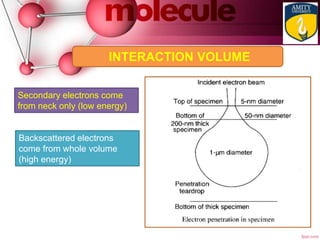
  • 22. INTERACTION VOLUME Backscattered electrons come from whole volume (high energy) Secondary electrons come from neck only (low energy)
  • 23. Fracture Surface in iron SECONDARY ELECTRONS BACKSCATTERED ELECTRONS CHOOSE CORRECT DETECTOR- TOPOGRAPHY EXAMPLE
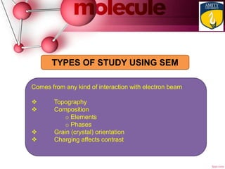
  • 24. Comes from any kind of interaction with electron beam  Topography  Composition o Elements o Phases  Grain (crystal) orientation  Charging affects contrast TYPES OF STUDY USING SEM
  • 26. RESOLUTION – DETERMINED BY PROBE SIZE
  • 27. RESOLUTION – PROBE DIAMETER & PROBE SIZE
  • 28. d = depth of field  = required spatial resolution a = convergence angle  d region of image in focus tana  0.5 0.5d   d For small angles, tana = a d   a Can control depth of field (d) with convergence angle (a) DEPTH OF FIELD