SlideShare a Scribd company logo
1
Memory & Programmable Logic
Logic and Digital System Design - CS 303
Erkay Savaş
Sabancı University
02/13/17 CS 303
2
Memory Unit
• A device
– to which binary information is transferred for storage
and
– from which information is available when needed for
processing
• When data processing takes place
– information from the memory is transferred to
selected register in the processing unit
– Intermediate and final results obtained in the
processing unit are transferred back to the memory
for storage
02/13/17 CS 303
3
Memory Unit
• Used to communicate with an input/output device
– binary information received from an input device is
stored in memory
– information transferred to an output device is taken
from memory
• A collection of cells capable of storing a large
quantity of binary information
• Two types
– RAM (random-access memory)
– ROM (read-only memory)
02/13/17 CS 303
4
Classification
• RAM
– We can read stored information (read operation)
– Accepts new information for storage (write operation)
– Perform both read and write operation
• ROM
– only performs read operation
– existing information cannot be modified
– “Programming” the device
• specifying the binary information and storing it
within the programmable device
– a.k.a. programmable logic device
02/13/17 CS 303
5
Programmable Logic Devices
• PLD
– ROM is one example
– Programmable Logic Array (PLA)
– Programmable Array Logic (PAL)
– Field Programmable Gate Array (FPGA)
• PLD is
– an integrated circuit (IC) with internal logic gates
– Interconnection between the gates can be
programmed through fuses
– At the beginning they are all intact
– By programming we remove some of them, while
keeping the others
02/13/17 CS 303
6
Random Access Memory (RAM)
• RAM
• The reason for the name
– The time it takes to transfer information to or from
any desired random location is always the same.
• Word
– groups of bits in which a memory unit stores
information
– At one time, memory move in and out of the storage a
word of information
– 8 bit – byte
– 16 bit
– 32 bit
– Capacity is usually given in number of bytes
02/13/17 CS 303
7
Memory Unit
• Block diagram
Memory Unit
2k
words
n bit per word
n data input lines
k address lines
Read
Write
n data output lines
Read/Write
02/13/17 CS 303
8
Specification
• A memory unit is specified by
1. the number of words it contains
2. number of bits in each word
• Each word (or location for a word) in memory is
assigned an identification number
– address
– 0 to 2k
-1
• Selection
– selection process to read and write a word is done by
applying k-bit address to the address lines
– A decoder accepts the address and selects the
specified word in the memory
02/13/17 CS 303
9
Memory Map and Address Selection
0xFC12
0x45AB
0xE24F
0x71C3
0x201D
0x092F
0000000000
0000000001
0000000010
0000000011
1111111111
1111111110
10 x 1024
Decoder
address
lines
1 K = 210
1 M = 220 1 G = 230
1 T = 240
• 1 K x 16 Memory
02/13/17 CS 303
10
Write and Read Operations
• Write
– transfer in
• Read
– transfer out
• Steps for write operation
1. Apply the binary address of the desired word to the
address lines
2. Apply the data word that is be stored in memory to
the (data) input lines
3. Activate the “write” input
02/13/17 CS 303
11
Read Operation
• Steps
1. Apply the binary address of the desired word to the
address lines
2. Activate the “read” input
– The desired word will appear on the (data) output
lines
– reading does no affect the content of the word
02/13/17 CS 303
12
Control Inputs to Memory Chip
• Commercial memory components usually provide a
“memory enable” (or “chip select”) control input
• memory enable is used to activate a particular
memory chip in a multi-chip implementation of a
large memory
Memory Enable Read/Write Memory Operation
0 X None
1 0 write
1 1 read
02/13/17 CS 303
13
Timing
• Memory does not have to use an internal clock
– It only reacts to the control inputs, e.g., “read” and
“write”
– operation of a memory unit is controlled by an external
device (e.g. CPU) that has its own clock
• Access time
– the time required to select a word and read it
• Cycle time
– the time required to complete a write operation
data
CPU Memory
address
read/write
enable
02/13/17 CS 303
16
Types of Memory 1/2
• RAM
– access time is always the same no matter where the
desired data is actually located
• Sequential-access memory
– Access time is variable
– e.g., magnetic disks, tapes
• RAM
– SRAM (static RAM)
• latches, stores information as long as power is on
– DRAM (dynamic RAM)
• information is stored as charge on a capacitor
• refreshing is necessary due to discharge02/13/17 CS 303
17
Types of Memory 2/2
• Volatile memory
– When the power is turned off, the stored information
is lost
– RAM (SRAM or DRAM)
• Nonvolatile memory
– retains the stored information after removal of power
– magnetic disks
• data is represented as the direction of
magnetization
– ROM
• programs needed to start a computer are kept in
ROM
02/13/17 CS 303
18
Memory Cell
• Equivalent logic of a memory cell for storing one
bit of information
S
R
output
input
read/write
select
BCinput
select
output
read/write
02/13/17 CS 303
S R Q(t+1)
0 0 Q
0 1 0
1 0 1
1 1 X
Q
19
4 x 4 RAM
read/write
input data
BCBC BC BC
BC BC BC BC
BC BC BC BC
BC BC BC BC
output data
2x4
decoder
word 0
word 1
word 2
word 3
EN
memory
enable
Address
inputs
02/13/17 CS 303
20
4 x 4 RAM
read/write
input data
BCBC BC BC
BC BC BC BC
BC BC BC BC
BC BC BC BC
output data
2x4
decoder
word 0
word 1
word 2
word 3
EN
memory
enable
Address
inputs
0
1
x3 x2 x1 x0
0 0 0 0
0 0 0 0
0 0 0 0
x3 x2 x1 x0
02/13/17 CS 303
21
Commercial RAMs
• Physical construction
– Capacity of thousands of words
– each word may range from 1 to 64 bits
• Example:
– We have memory chips of 1024×4
– Logical construction: 1024×8
1024×4
address
lines
memory enable
read/write
1024×4
data output
data input
02/13/17 CS 303
22
Combining Memories
2048×4 RAM
Memory
Enable
1024×4
address
lines
ME
R/W
1024×4
ME
R/W
...
...
0
1
9
0
1
9
X
X
.
X
0
X
X
.
X
1
02/13/17 CS 303
23
Coincident Decoding
• A memory with 2k
words requires a k × 2k
decoder
• k × 2k
decoder requires 2k
AND gates with k
inputs per gate
• There are ways to reduce the total number of
gates and number of inputs per gate
• Two dimensional selection scheme
– Arrange the memory words in an array that is as close
as possible to square
– Use two k/2-input decoders instead of one k-input
decoder.
• One decoder performs the row selection
• The other does the column selection
02/13/17 CS 303
24
Example: Coincident Decoding
5×32
decoder
X
0
1
2
12
31
5×32
decoder
0 1 2 20 31
Y
01100 10100
Binary address
1024 word memory
02/13/17 CS 303
25
DRAMs
• SRAM memory is expensive
– One cell typically contains four to six transistors
– Usually used for on-chip cache memories and
embedded systems (cameras, smart phones, etc.)
• DRAM is much less expensive
– One MOS transistor and a capacitor
– Four times the density of SRAM in a given chip area
– cost per bit storage is three to four times less than
SRAM
– low power requirement
– Perfect technology for large memories such as main
memory
– Most DRAMs have short word sizes02/13/17 CS 303
28
Read-Only Memory
• ROM
– memory device in which permanent binary information
is stored
– Binary information must be specified by the designer
– It then is embedded in the unit to form the required
interconnection pattern
– nonvolatile
• Block diagram
2k
x n
ROM
k inputs n outputs
• no data inputs
• enable inputs
• three-state outputs
Programming input
02/13/17 CS 303
29
Example: ROM
• 32 x 8 ROM
5x32
decoder
0
1
2
3
31
30
29
28
I0
I1
I2
I3
I4
A0A1
A2A3A4A5
A6A7
each OR gates
are considered as
having 32 inputs
intersections
02/13/17 CS 303
30
Example: ROM
• Number of connections
– 32 × 8 ROM has 32 × 8 = 256 internal connections
• In general
– 2k
× n ROM will have a k × 2k
decoder and n OR gates
– Each OR gate has 2k
inputs
– inputs of every OR gate are initially connected to each
output of the decoder
• These intersections are programmable
– they are initially closed (connected to the input of OR
gate)
– A fuse is used to connect two wires
– During programming, some of these fuses are blown by
applying high voltage.
02/13/17 CS 303
31
Programming ROM
• Internal storage specified by a table
• Example: 32 × 8 ROM
Inputs Outputs
I4 I3 I2 I1 I0 A7 A6 A5 A4 A3 A2 A1 A0
0 0 0 0 0 1 0 1 1 0 1 1 0
0 0 0 0 1 0 0 0 1 1 1 0 1
0 0 0 1 0 1 1 0 0 0 1 0 1
0 0 0 1 1 1 0 1 1 0 0 1 0
… … … … … … … … … … … … …
1 1 1 0 0 0 0 0 0 1 0 0 1
1 1 1 0 1 1 1 1 0 0 0 1 0
1 1 1 1 0 0 1 0 0 1 0 1 0
1 1 1 1 1 0 0 1 1 0 0 1 1
02/13/17 CS 303
32
Programming ROM
5x32
decoder
0
1
2
3
31
30
29
28
I0
I1
I2
I3
I4
A0A1
A2A3
A4A5
A6A7
Inputs Outputs
I4 I3 I2 I1 I0 A7 A6 A5 A4 A3 A2 A1 A0
0 0 0 0 0 1 0 1 1 0 1 1 0
.02/13/17 CS 303
33
Combinational Circuit Design with ROM
• Formerly,
– we have shown that a k × 2k
decoder generates 2k
minterms of k input variables
• Furthermore,
– by inserting OR gates to sum these minterms, we were
able to realize any desired combinational circuit.
• A ROM is essentially a device that includes both
the decoder and the OR gates within a single
device.
– first interpretation: a memory unit that stores words
02/13/17 CS 303
34
Combinational Circuit Design with ROM
• ROM (cont.)
– Second interpretation: a programmable device that
can realize any combinational circuit
5x32
decoder
0
1
2
3
31
30
29
28
I0
I1
I2
I3
I4
A0A1
A2A3
A4A5
A6A7
02/13/17 CS 303
35
Combinational Circuit Design with ROM
• Example: Truth table
Inputs Outputs
A2 A1 A0 B5 B4 B3 B2 B1 B0
0 0 0 0 0 0 0 0 0
0 0 1 0 0 0 0 1 1
0 1 0 0 0 0 1 0 0
0 1 1 0 0 1 0 1 0
1 0 0 0 1 0 0 0 0
1 0 1 0 1 1 0 0 1
1 1 0 1 0 0 1 1 1
1 1 1 1 1 0 0 0 1
02/13/17 CS 303
36
Example: Design with ROM
8 x 6 ROM would suffice
ROM Truth Table
8 × 6
ROM
A2
A1
A0
B4
B3
B2
B5
B1
B0
Inputs Outputs
A2 A1 A0 B5 B4 B3 B2 B1 B0
0 0 0 0 0 0 0 0 0
0 0 1 0 0 0 0 1 1
0 1 0 0 0 0 1 0 0
0 1 1 0 0 1 0 1 0
1 0 0 0 1 0 0 0 0
1 0 1 0 1 1 0 0 1
1 1 0 1 0 0 1 1 1
1 1 1 1 1 0 0 0 1
02/13/17 CS 303
Example: Design with ROM
37
3x8
decoder
0
1
2
3
7
6
5
4
I0
I1
I2
B0B1
B2B3
B4B5
Inputs Outputs
A2 A1 A0 B5 B4 B3 B2 B1 B0
0 0 0 0 0 0 0 0 0
0 0 1 0 0 0 0 1 1
0 1 0 0 0 0 1 0 0
0 1 1 0 0 1 0 1 0
1 0 0 0 1 0 0 0 0
1 0 1 0 1 1 0 0 1
1 1 0 1 0 0 1 1 1
1 1 1 1 1 0 0 0 1
02/13/17 CS 303
38
Types of ROM 1/2
• Programming can be done in different ways
– Mask programming:
• customer provides the truth table
• manufacturer generates the mask for the truth table
• can be costly, since generating a custom mask is
charged to the customer.
• economical only if a large quantity of the same ROM
configuration is to be ordered.
– Field Programmable
• Programmable ROM (PROM):
• Customer can program the ROM by blowing fuses by
applying high voltage through a special pin
• Special instrument called PROM programmer is
needed.02/13/17 CS 303
39
Types of ROM 2/2
• Programming ROM and PROMs is irreversible.
• Erasable PROM (EPROM)
– can be programmed repeatedly.
– EPROM is placed under a special
ultra-violet light for a given period of time
– At the end, the former program is erased
– After erasure, EPROM becomes ready for another
programming
• Electronically erasable PROM
(EEPROM or E2
PROM)
02/13/17 CS 303
40
Programmable Logic Devices
• EPROM is an example of combinational
programmable logic device (PLD)
• Configuration of EPROM
Outputs
Fixed
AND array
(decoder)
programmable
OR arrayInputs
02/13/17 CS 303
41
Other PLDs
• Two other types
Outputs
Programmable Array Logic (PAL)
programmable
AND array
fixed
OR arrayInputs
Inputs
programmable
AND array
programmable
OR array
Outputs
Programmable Logic Array (PLA)
02/13/17 CS 303
42
Programmable Logic Array (PLA)
• Similar to PROM
• However, PLA does not generate all the minterms
• Decoder is replaced by an array of AND gates
– can be programmed to generate any product term of
input variables
• The product terms are then connected to OR
gates
– that provide the sum of products
Inputs
programmable
AND array
programmable
OR array
Outputs
02/13/17 CS 303
43
PLA: Example
• PLA: 3 inputs, 5 product terms and 4 outputs
F1
F2
A
B
C
A’AB’BC’C
0
1
F1 = (A + B’C’)’
F2 = AC’ + AB
F3 = B’C’ + AB
F4 = B’C + A
F3
F4
F1 = A’B + A’C
02/13/17 CS 303
44
PLA Programming Table
Outputs
Inputs C T
Product Term A B C F1 F2 F3 F4
1 1 - - 1
2 - 0 0 1
3 1 - 0 -
4
5
F1 = (A + B’C’)’
F2 = AC’ + AB
F3 = B’C’ + AB
F4 = B’C + A
http://tams-www.informatik.uni-hamburg.de/applets/hades/webdemos/42-
programmable/10-pla/pla.html
02/13/17 CS 303
45
Size of PLA
• Specified by
– number of inputs, number of product terms, number of
outputs
• A typical IC PLA (F100)
– 16 inputs, 48 product terms, and 8 outputs
• n input, k product terms, m output PLA has
– k AND gates, m OR gates, m XOR gates
– 2n × k connections between input and the AND array
– k × m connections between the AND and OR arrays
– 2m connections associated with XOR gates
– (2n × k + k × m + 2m) connections to program
02/13/17 CS 303
46
PLA: Example
• PLA: 3 inputs, 5 product terms and 4 outputs
F1
F2
A
B
C
A’AB’BC’C
0
1
F1 = (A + B’C’)’
F2 = AC’ + AB
F3 = B’C’ + AB
F4 = B’C + A
F3
F4
02/13/17 CS 303
47
Programming PLA
• Optimization
– number of literals in a product term is not important
– When implementing more than one function, functions
must be optimized together in order to share more
product terms
• multiple output optimization (espresso)
– both the true and complement of each function should
be simplified to see which one requires fewer number
of product terms
http://diamond.gem.valpo.edu/~dhart/ece110/espresso/tutorial.html
02/13/17 CS 303
48
Example: Programming PLA
• Two functions
– F1 (A, B, C) = Σ(0, 1, 2, 4)
– F2 (A, B, C) = Σ(0, 5, 6, 7)
BC
A 00 01 11 10
0 1 1 0 1
1 1 0 0 0
BC
A 00 01 11 10
0 1 0 0 0
1 0 1 1 1
F1 = A’B’ + A’C’ + B’C’
F1 = (AB + AC + BC)’
F2 = AB + AC + A’B’C’
F2 = (A’C + A’B + AB’C’)’
02/13/17 CS 303
49
Example: Programming PLA
• PLA programming table
Outputs
Inputs
Product Term A B C F1 F2
AB 1 1 1 -
AC 2 1 - 1
BC 3 - 1 1
A’B’C’ 4 0 0 0
F1 = (AB + AC + BC)’
F2 = AB + AC + A’B’C’
02/13/17 CS 303
50
Programmable Array Logic (PAL)
• Easier to program than PLA
• But, not as flexible
• A typical PAL
– 8 inputs, 8 outputs, 8-wide AND-OR array
Outputs
Programmable Array Logic (PAL)
programmable
AND array
fixed
OR arrayInputs
02/13/17 CS 303
51
Example: PAL
F1
F2
F3
F4
I1
I2
I3
I4
AND gates inputs
1
2
3
4
5
6
7
8
9
10
11
12
product
term
02/13/17 CS 303
52
Design with PAL
• Each Boolean function must be simplified to fit
into each section.
• Product terms cannot be shared among OR gates
– Each function can be simplified by itself without
regard to common product terms
• The number of product terms in each section is
fixed
– If the number of product terms is too many, we may
have to use two sections to implement the function.
02/13/17 CS 303
53
Example: Design with PAL
• Four functions
– A(x, y, z, t) = Σ (2, 12, 13)
– B(x, y, z, t) = Σ (7, 8, 9, 10, 11, 12, 13, 14, 15)
– C(x, y, z, t) = Σ (0, 2, 3, 4, 5, 6, 7, 8, 10, 11, 15)
– D(x, y, z, t) = Σ (1, 2, 8, 12, 13)
• First step is to simplify four functions separately
– A = xyz’ + x’y’zt’
– B = x + yzt
– C = x’y + zt + y’t’
– D = xyz’ + x’y’zt’ + xy’t’ + x’y’z’t
02/13/17 CS 303
Example:
Design with
PAL
54
F1
F2
F3
F4
x
y
z
1
2
3
4
5
6
7
8
9
10
11
12
A = xyz’ + x’y’zt’
B = x + yzt
C = x’y + zt + y’t’
D = xyz’ + x’y’zt’ + xy’t’ + x’y’z’t = A + xy’t’ + x’y’z’t
02/13/17 CS 303t
55
Example: Design with PAL
– D = A + xy’t’ + x’y’z’t
12
11
10
-0-0-9
-11--8
---107
-----6
-111-5
----14
-----3
-01002
--0111
D = F4 = F1
+ xy’t’
+ x’y’z’t
C = F3 = x’y
+ zt
+ y’t’
B = F2 = x
+ yzt
A = F1 = xyz’ +
x’y’zt’
F1tzyx Outputs
AND InputsProduct
Term
02/13/17 CS 303
56
Example: Design with PAL
A
B
C
D
x
y
z
t
AND gates inputs
x x’ y y’ z z’ t t’ A A’
1
2
3
4
5
6
7
8
9
10
11
12
A = xyz’ + x’y’zt’
D = A + xy’t’ + x’y’z’t
02/13/17 CS 303
57
PAL: BCD to 7-Segment
-Display Decoder
• (ABCD)10  (a b c d e f g)
a
g
d
b
ce
f
BCD to
7-segment-display
decoder
DCBA
a b c d e f g
– a = A + BD + C + B’D’
– b = A + C’D’ + CD + B’
– c = A + B + C’
– d = B’D’ + CD’ + BC’D + B’C
– e = B’D’ + CD’
– f = A + C’D’ + BD’ + BC’
– g = A + CD’ + BC’ + B’C
– we need 4 inputs, 7 outputs,
4 product terms per output
– P16H8: 10 inputs, 8 outputs,
7 product terms per output
P14H8: 14 inputs,
8 outputs (2 have four
product terms, 6 have
2 product terms)
02/13/17 CS 303
58
7-Segment-Display Decoder
• Different way to optimize
– multiple output optimization  espresso supports this
– a = BC’D + CD + B’D’ + A + BCD’
– b = B’D + C’D’ + CD + B’D’
– c = B’D + BC’D + C’D’ + CD + BCD’
– d = B’C + BC’D + B’D’ + BCD’
– e = B’D’ + BCD’
– f = BC’D + C’D’ + A + BCD’
– g = BC’ + B’C + A + BCD’
– 9 product terms in total (previous one has 14)
• PLA can also be used
– F100: 16 inputs, 48 product terms, and 8 outputs
– a = A + BD + C + B’D’
– b = A + C’D’ + CD + B’
– c = A + B + C’
– d = B’D’ + CD’ + BC’D + B’C
– e = B’D’ + CD’
– f = A + C’D’ + BD’ + BC’
– g = A + CD’ + BC’ + B’C
02/13/17 CS 303
59
Sequential PLDs
• So far, we have seen PLD that can realize only
combinational circuits
• However, digital systems are designed using
both combinational circuits (gates) and flip-
flops.
– With PLDs, we need to use external flip-flops to
realize sequential circuit functions.
• Different types
1. Sequential (or simple) programmable logic device
(SPLD)
2. Complex programmable logic device (CPLD)
3. Field programmable gate array (FPGA)
02/13/17 CS 303
60
SPLD
• Additional programmable connections are available to
include flip-flop outputs in the product terms formed
with AND array.
• Flip-flops may be of D or JK type
• Example: AMD 22V10
– 24 pin device, 10 output logic macrocells
– The number of product term allocated to an output varied from 8
to 16
Inputs
Outputs
Sequential Programmable Logic Device (SPLD)
programmable
AND-OR array
(PAL or PLA) flip-flops
02/13/17 CS 303
AMD 22V10
02/13/17 CS 303 61
62
SPLD Macrocell
• SPLD is usually PAL + D flip-flops
• Each section in SPLD is called macrocell.
• A macrocell
– sum-of-products combinational logic + optional flip-flop
– 8-10 macrocells in one IC package
CLK OE
D Q
C
x
y
x x’ y y’02/13/17 CS 303
63
Additional SPLD Functionalities
• Additional SPLD Functionalities
– Bypass circuitry for the output (bypassing) flip-flop
– selection of clock edge polarity
– XOR gate for selection of true or complement of
output
D Q
C
x
y
CLK
OE
CLK OEx x’ y y’ Q Q’
bypass
0
1
02/13/17 CS 303
Example: serial adder
• Output equation:
– S = x ⊕ y ⊕ Q = x’y’Q + x’yQ’ + xyQ + xy’Q’
• Flip-flop input equation:
– D = Q(t+1) = xy + xQ + yQ
64
6464
shift register A
shift register B
SI
FA
a
b
C_in
S
C
DQ
C
SO
SO
SIserial
input
clock
shift
control
reset
serial
output
02/13/17 CS 303
65
Example: Serial Adder with SPLD
Q(t+1) = xy + xQ + yQ
D Q
C
x
y
CLK
OE
CLK OEx x’ y y’ Q Q’
bypass
0
1
02/13/17 CS 303
66
Example: Serial Adder with SPLD
• S = x’y’Q + x’yQ’ + xyQ + xy’Q’
D Q
C
x
y
CLK
OE
CLK OEx x’ y y’ Q Q’
bypass
0
1
02/13/17 CS 303
Generic Array Logic (GAL)
• Similar to SPLD with PAL
– PAL uses fuses while GAL uses electrically erasable
CMOS (E2CMOS) cell at each intersection
6702/13/17 CS 303
68
Complex Programmable Logic Device
PLD PLD PLD PLD
PLD PLD PLD PLD
programmable switch matrix
IO
block
IO
block
Example: Altera MAX 7000-series CPLD with 2500 gates
02/13/17 CS 303
69
FPGA
• Field Programmable Gate Array
– FPGA is a VLSI circuit
– Field programmable means user can program it in his
own location
– Gate array consists of a pattern of gates fabricated in
an area of silicon
• pattern of gates are repeated many (thousand)
times
– one thousand to millions of gates are fabricated within
a single IC chip
02/13/17 CS 303
Basics of FPGA
7002/13/17 CS 303
71
Basics of FPGA
CLB
CLB
PSM PSM
PSM PSM
CLB
CLB CLB
CLB CLB
CLBCLBCLB
02/13/17 CS 303
72
Basics of FPGA
• A typical FPGA consists of an array of hundreds
or thousands of configurable logic blocks (CLB)
– CLBs are connected to each other via programmable
interconnection structure
– CLBs are surrounded by I/O blocks for basic
communication with outside world.
• CLBs consist of look-up tables, multiplexers,
gates, and flip flops
• look-up table
– is a truth table stored in an SRAM
– provides the combinational circuit functions for the
logic block.
– It is like a ROM implemented as SRAM02/13/17 CS 303
73
Xilinx FPGA – CLB (Partial View)
MUX
0
1
2
3
1 1
a
b
c
d
y=d
SRAM Cells
Lookup Table
(LUT)
A
B
C
D
G
F
D Q
X
Y
S
R
K
2
1
0
2
1
0
2
1
0
02/13/17 CS 303
74
Inside CLB
• Lookup Table
– 16 × 2 ROM (implemented as SRAM)
– Implements two four-variable Boolean functions
– Can also be configured as memory (RAM)
• Multiplexers
– 2k
input multiplexers
– controlled by k SRAM cells
• Flip-flop
– provides operation as a sequential system
– can be configured as a latch as well.
02/13/17 CS 303
Xilinx XC 4000 CLB
75
G4
G3
G2
G1
F4
F3
F2
F1
Logic
Function
of
G1 – G4
Logic
Function
of
F’, G’, H1
Logic
Function
of
F1 – F4
G
F
DIN
F ’
G ’
H ’
DIN
F ’
G ’
H ’
H H ’
G ’
K (clock)
EC
D Q
SD
RD
1
S/R
Control
S/R
Control
EC
D Q
SD
RD
1
H1
DIN / H2 SR /
H0
EC
H ’
F ’
4
C1 … C4
bypass
X
Y
XQ
YQ
02/13/17 CS 303
Lookup Tables (LUT)
• Combinational circuits are implemented using LUT
76
y
A
B
C
D
G4(A) G3(B) G2(C) G1(D) G(y)
0 0 0 0 0
0 0 0 1 1
0 0 1 0 1
0 0 1 1 1
0 1 0 0 0
0 1 0 1 1
0 1 1 0 1
0 1 1 1 1
1 0 0 0 0
1 0 0 1 1
1 0 1 0 1
1 0 1 1 1
1 1 0 0 0
1 1 0 1 0
1 1 1 0 0
1 1 1 1 0
G4
G3
G2
G1
Logic
Function
of
G1 – G4
G
02/13/17 CS 303
LUT
• Using three function generators F, G, and H
– A single CLB can implement any Boolean function of
five variables
• General form of Boolean function of five variables:
H = F(x, y, z, t)·w’+ G(x, y, z, t )·w
– Some functions of up to nine variables
• Nine logic inputs: F1, F2, F3, F4, G1, G2, G3, G4, and H1.77
G4
G3
G2
G1
F4
F3
F2
F1
Logic
Function
of
G1 – G4
Logic
Function
of
F, G, H1
Logic
Function
of
F1 – F4
G
F
H
H1
F
G
02/13/17 CS 303
Logic
Function
of
G1 – G4
Logic
Function
of
F, G, H1
Logic
Function
of
F1 – F4
G
F
H
w
F
G
x
y
z
t
H
w’
F
w
G
LUT as Memory
• LUTs can be configured as memory block
– One 16x2 memory module
– One 32x1 memory module
– Dual-ported 16x1 memory module
– Synchronous-edge-triggered and asynchronous-
memory interfaces are supported
02/13/17 78CS 303
G4
G3
G2
G1
F4
F3
F2
F1
Logic
Function
of
G1 – G4
Logic
Function
of
F1 – F4
G
F
F
G
LUT as Memory
79
G4
G3
G2
G1
F4
F3
F2
F1
G
F
16x2 configuration
Address
G4
G3
G2
G1
F4
F3
F2
F1
G
F
16x1 dual-ported configuration
Address
One write
02/13/17 CS 303
LUT as Memory
80
G4
G3
G2
G1
F4
F3
F2
F1
G
F
16x2 configuration
Address
G4
G3
G2
G1
F4
F3
F2
F1
G
F
16x1 dual-ported configuration
Address
1
Address
2
Two reads at the same time
02/13/17 80CS 303
LUT as Memory
81
32x1 configuration
G4
G3
G2
G1
F4
F3
F2
F1
G
F
0
1
A4
A3
A2
A1
A0
Address
02/13/17 CS 303
Distributed RAM
8202/13/17 CS 303
Spartan Dual-Port RAM
8302/13/17 CS 303
A Simple Memory on FPGA
module simple_memory(clk, reset, dat_in, wr_adr, wr_en, dat_out,
rd_adr);
input clk, reset;
input [15:0] dat_in;
input [7:0] wr_adr;
input wr_en;
output [15:0] dat_out;
input [7:0] rd_adr;
// synthesis attribute ram_style of my_memory is block
reg [15:0] my_memory[0:255];
reg [15:0] dat_out;
always @(posedge clk)
begin
if(wr_en)
my_memory[wr_adr] <= dat_in;
dat_out <= my_memory[rd_adr];
end
endmodule
02/13/17 CS 303 84
85
Switch Matrix
• Different levels of interconnections
– Direct interconnects between CLBs. Short wires to
connect adjacent CLBs in both directions.
– Switch matrix
CLB CLB CLB
CLB CLB CLB
CLB CLB CLB
PSM PSM
PSM PSM
• PSM: Programmable
Switch Matrix
• PSM can be configured to
connect a horizontal wire
to a vertical one.
• One wire can be
connected to multiple
wires
• This way output of a CLB
can be routed through
multiple PSMs to the input
of another CLB.02/13/17 CS 303
86
PSM
CLB
12 4 4
2
2
12
6 4 8 4
8
4
3
3
Quad
Single
Double
long
Direct
connect
long
long long DoubleQuad Direct
connect
Carry
chain
Single Global
clock
Global
clock
02/13/17 CS 303
87
Types of Lines
• Single-length: connects adjacent PSMs
• Double-length: connects every other PSM
• Quad-length: traverse four CLBs before passing through
a PSM.
• Long: runs entire chip.
– Using tri-state buffers within the CLBs, long lines can be
configured as buses.
• Local connections use direct interconnect or single length
lines in order to avoid to many switching points
• Global Nets: Low skew signal paths used to distribute
high fan-out signals such as clock and reset signals.
02/13/17 CS 303
88
Double Length Lines
CLB
CLB CLB
CLB CLB CLB
CLB CLB CLB
PSM PSM
PSM PSM
PSM
PSM
02/13/17 CS 303
89
Example Interconnects
Direct interconnects
between adjacent CLBs
CLB CLB CLB
CLB CLB CLB
CLB CLB CLB
PSM PSM
PSM PSM
PSM PSM
CLB
CLB CLB
CLB
General-purpose
interconnects
02/13/17 CS 303
90
4-bit Adder with CLBs 1/2
X0 Y0 Cin
Z0
CLB
A B C D
xy
C1
CLB
X1 Y1
Z1
A B C D
xy
C2
CLB
X2 Y2
Z2
A B C D
xy
CLB
X3 Y3
Z3
A B C D
xy
C3
C4
02/13/17 CS 303
91
4-bit Adder with CLBs 2/2
CLB
X0 Y0
Z0
A B C D
xy
C1
X1 Y1
C2
X2 Y2
Z1Z2
02/13/17 CS 303
Spartan II Architecture
9202/13/17 CS 303
Xilinx Spartan II Characteristics
• Density: up to 200,000 system gates
– Up to 5292 logic cells
– Each cell contains a LUT
• Operating voltage: 2.5 V
• Operating frequency: 200 MHz
• On-chip block memory
– not made up of look-up tables
– Does not reduce the amount of logic
– Improve performance by reducing the need to access
off-chip storage.
• 0.22/0.18-µm CMOS technology
– Six layers of metal for interconnect 9302/13/17 CS 303
Xilinx Spartan II Characteristics
• Reliable clock distribution
– Clock synchronization through delay-locked loops
(DLLs)
– DLLs eliminate clock distribution delay
– DLLs provide frequency multipliers, frequency dividers
• Different architecture
– Four quadrants
– Each quadrant is associated with 4096-bit block RAM
– There are FPGAs with up to 14 blocks of block RAM
(56K bits total block memory)
9402/13/17 CS 303
Slice
95
• A logic cell contains
a four-input lookup
table, logic for carry
and control and a
D type flip-flop
• Each slice contains
contains two cells
• Each CLB contains
two slices.
02/13/17 CS 303
Carry Logic
• Lookup tables can be used to generate the sum
bits.
• Each slice can be programmed to implement both
carry and sum for two bits.
• The carry lines between cells are hardwired (not
programmed) to provide for fast propagation of
carries
• The carry logic can be programmed to implement
subtracter, incrementer/decrementers, 2’s
complementers, and counters
9602/13/17 CS 303
A Slice as Two-Bit Full Adder
G2: Ai+1
G1: Bi+1
Ci
G Function
F Function
Carry Logic
Si+1
Si
Ci+2
Ci+1
F2: Ai
F1: Bi
hardwired
02/13/17 CS 303
Connections for 4-bit Adder
9898
Slice
Slice
A1
B1
A0
B0
C0
C2
C3
A3
B3
A2
B2
Hard-
wired
• If we want to detect a
possible overflow, we add
the 4th
Slice.
• The 3rd
Slice outputs C3
instead of C4 (How?)
• In the 4th
Slice, C4 can be
re-computed using the
carry logic.
• Overflow is computed using
the G function generator in
the 4th
Slice
• Overflow: V = C3 ⊕ C4
• 4-bit adders can easily be
expanded 8 or 16-bit
adders
• Adder modules are available
in Xilinx library
Slice C4
V
02/13/17 CS 303
Core Generators
• Many vendors typically supply implementation of
common building blocks that are optimized to the
structure of their hardware components.
– Xilinx, in fact, has a core generator utility that can
create common building blocks from parameterized
descriptions provided by the user
– Adders, subtractors, multipliers, memories, etc. are
such building blocks
• FPGA as a sea of LUTs and flip-flops
– A gate-level design can be placed on the array by
mapping combinational components to LUTs, sequential
to flip-flops
9902/13/17 CS 303
Adder/Subtracter with Core
Generator
02/13/17 CS 303 100
Divider with Core Generator
02/13/17 CS 303 101
Multiplier with Core Generator
02/13/17 CS 303 102
Xilinx Virtex FPGAs
• Leading edge of Xilinx technology
– 65 nm technology
– 1 V operating voltage
– Up to 330,000 logic cells
– Over 200,000 internal flip-flops
– 10 Mb of block RAM
– Hardwired units: multipliers, DSP units,
microprocessors (powerPC)
– 550-MHz clock technology
10302/13/17 CS 303
Xilinx Virtex FPGAs
10402/13/17 CS 303
105
Design with Programmable Devices
• Requires CAD tools
• Entry tools: entering a design
– schematic entry package
– FSM (finite state machine)
– Hardware description languages (HDL)
• VHDL, Verilog, ABEL,
• Synthesis tools
– allocate
– map
– configure
– connect logic blocks
02/13/17 CS 303
106
FPGA Design Flow 1/4
HDL
editor
State machine
editor
Schematic
capture
Synthesis
Place and Route
Programming
Behavioral simulation
Functional simulation
Verification
Device programmingXilinx Tools
Core
Generation
Utilities
Model Development
02/13/17 CS 303
107
FPGA Design Flow 2/4
• Model development:
– VHDL code
– State-machines may be described in a graphical manner and
translated into VHDL code.
– Traditional schematic capture can be translated into VHDL
source.
• Behavioral Simulation
– Before synthesis; for testing functional correctness
• Synthesis
– The design is synthesized to a library of primitive components
such as gates, flip-flops, and latches
• Functional Simulation
– To find out preliminary performance estimates
– For example, timing information can be obtained from known
properties of FPGA components
– Still not too accurate
02/13/17 CS 303
108
FPGA Design Flow 3/4
• Place and Route:
– The design is mapped to the primitives in the target
chip
– In FPGA, there are function generators (LUTs), flip-
flops, and latches
– Each primitive must be assigned to a specific CLB
(Placement)
– Connections between CLBs that implement the
primitives must be established (routing)
– Accurate timing can be obtained in Verification step
(Post-placement and routing simulation)
– The configuration bits are generated.
02/13/17 CS 303
109
FPGA Design Flow 4/4
• Programming:
– The configuration data (bit stream) is finally loaded
into the target FPGA chip.
• These steps are fairly generic although the
terminology used here is adopted from Xilinx.
02/13/17 CS 303
110
Xilinx Tools: Design Flow
02/13/17 CS 303

More Related Content

PDF
Introduction to pic microcontroller
PPT
Microcontroller 8051
PPTX
PPTX
Ardui no
PPTX
10 chapter05 counters_fa14
PPTX
Hardware View of Intel 8051
PPT
8051 Microcontroller
PPTX
Pic 18 microcontroller
Introduction to pic microcontroller
Microcontroller 8051
Ardui no
10 chapter05 counters_fa14
Hardware View of Intel 8051
8051 Microcontroller
Pic 18 microcontroller

What's hot (20)

PDF
Dcs lec03 - z-analysis of discrete time control systems
PDF
Embedded system introduction - Arduino Course
PPT
Memory organization of 8051
PPTX
Pic microcontroller architecture
PPT
Microcontroller 8051
PPTX
ATMEGA 328
PPTX
Introduction to Arduino and Hands on to Iot
PPTX
PERMANENT MAGNET BRUSHLESS DC MOTOR
PDF
Introduction to Avr Microcontrollers
PDF
Arduino Workshop Day 2 - Advance Arduino & DIY
PPT
AVR Fundamentals
PPTX
HEARTBEAT RATE SENSOR USING MICROCONTROLLER
PPTX
Presentation On: "Micro-controller 8051 & Embedded System"
PPTX
Unit v memory &amp; programmable logic devices
PPTX
Lpc 1768 timers
PPTX
Automatic irrigation 1st review(ieee project ece dept)
PDF
Analysis and design of analog integrated circuits
PDF
pulse width modulated inverter techniques
PPT
Actuators.ppt
Dcs lec03 - z-analysis of discrete time control systems
Embedded system introduction - Arduino Course
Memory organization of 8051
Pic microcontroller architecture
Microcontroller 8051
ATMEGA 328
Introduction to Arduino and Hands on to Iot
PERMANENT MAGNET BRUSHLESS DC MOTOR
Introduction to Avr Microcontrollers
Arduino Workshop Day 2 - Advance Arduino & DIY
AVR Fundamentals
HEARTBEAT RATE SENSOR USING MICROCONTROLLER
Presentation On: "Micro-controller 8051 & Embedded System"
Unit v memory &amp; programmable logic devices
Lpc 1768 timers
Automatic irrigation 1st review(ieee project ece dept)
Analysis and design of analog integrated circuits
pulse width modulated inverter techniques
Actuators.ppt
Ad

Viewers also liked (20)

PPT
Comp Apps Presenation 1 Nitin Goel And Thalia Flores
PDF
Performance Analysis of Full Adder Based 2- Bit Comparator using Different De...
PPTX
Inside a computer
PPTX
ENVI- 1 introduction
PPTX
Basic structure of capacitor
PPTX
Chapter5
PPSX
8085 Interfacing with I/O Devices or Memory
DOCX
8085 interfacing with memory chips
PPTX
Automatic power factor correction
PPTX
Introduction of mechatronics
PPT
PPT
Automatic power factor controller by microcontroller
PPT
Nano robot / nano technology
PPTX
Reliability and yield
PPTX
Introduction to 3G
PPT
PDF
Micro-controller based Automatic Power Factor Correction System Report
PPTX
Power factor correction
Comp Apps Presenation 1 Nitin Goel And Thalia Flores
Performance Analysis of Full Adder Based 2- Bit Comparator using Different De...
Inside a computer
ENVI- 1 introduction
Basic structure of capacitor
Chapter5
8085 Interfacing with I/O Devices or Memory
8085 interfacing with memory chips
Automatic power factor correction
Introduction of mechatronics
Automatic power factor controller by microcontroller
Nano robot / nano technology
Reliability and yield
Introduction to 3G
Micro-controller based Automatic Power Factor Correction System Report
Power factor correction
Ad

Similar to Ch07 (20)

PPT
Lec17 Intro to Computer Engineering by Hsien-Hsin Sean Lee Georgia Tech -- Me...
PPTX
DIGITAL DESIGNS SLIDES 7 ENGINEERING 2ND YEAR
PPTX
unit 5 M PROGRAMMBLE LOGIC DEVICES (1).pptx
PDF
Esd mod 3
PPT
Module4
PPT
EPROM, PROM & ROM
PPT
computer chapter5-the memory system (1) (2).ppt
PPT
chapter5-the memory system chapter .ppt
PPT
memory systems-module 3 presentation ppt
PDF
Computer organization memory
PPT
Chapter5 the memory-system-jntuworld
PDF
EC8392 -DIGITAL ELECTRONICS -II YEAR ECE-by S.SESHA VIDHYA /ASP/ ECE/ RMKCET
PPTX
Introduction to the memory system embedded.pptx
PPT
Computer Organisation and Architecture
PPTX
Computer Architecture and Organization--Memory and I/O
PPTX
Memories in digital electronics
PPTX
Random Access Memory
PPTX
CST 20363 Session 4 Computer Logic Design
PPTX
Introduction to Embedded C++.pptx
PPTX
Unit IV Memory.pptx
Lec17 Intro to Computer Engineering by Hsien-Hsin Sean Lee Georgia Tech -- Me...
DIGITAL DESIGNS SLIDES 7 ENGINEERING 2ND YEAR
unit 5 M PROGRAMMBLE LOGIC DEVICES (1).pptx
Esd mod 3
Module4
EPROM, PROM & ROM
computer chapter5-the memory system (1) (2).ppt
chapter5-the memory system chapter .ppt
memory systems-module 3 presentation ppt
Computer organization memory
Chapter5 the memory-system-jntuworld
EC8392 -DIGITAL ELECTRONICS -II YEAR ECE-by S.SESHA VIDHYA /ASP/ ECE/ RMKCET
Introduction to the memory system embedded.pptx
Computer Organisation and Architecture
Computer Architecture and Organization--Memory and I/O
Memories in digital electronics
Random Access Memory
CST 20363 Session 4 Computer Logic Design
Introduction to Embedded C++.pptx
Unit IV Memory.pptx

Recently uploaded (20)

PPTX
Introduction to Child Health Nursing – Unit I | Child Health Nursing I | B.Sc...
PPTX
Week 4 Term 3 Study Techniques revisited.pptx
PPTX
Microbial diseases, their pathogenesis and prophylaxis
PDF
Insiders guide to clinical Medicine.pdf
PPTX
IMMUNITY IMMUNITY refers to protection against infection, and the immune syst...
PDF
The Lost Whites of Pakistan by Jahanzaib Mughal.pdf
PPTX
Final Presentation General Medicine 03-08-2024.pptx
PDF
Module 4: Burden of Disease Tutorial Slides S2 2025
PDF
Chapter 2 Heredity, Prenatal Development, and Birth.pdf
PDF
Abdominal Access Techniques with Prof. Dr. R K Mishra
PDF
TR - Agricultural Crops Production NC III.pdf
PDF
Anesthesia in Laparoscopic Surgery in India
PDF
BÀI TẬP BỔ TRỢ 4 KỸ NĂNG TIẾNG ANH 9 GLOBAL SUCCESS - CẢ NĂM - BÁM SÁT FORM Đ...
PPTX
PPT- ENG7_QUARTER1_LESSON1_WEEK1. IMAGERY -DESCRIPTIONS pptx.pptx
PDF
grade 11-chemistry_fetena_net_5883.pdf teacher guide for all student
PDF
2.FourierTransform-ShortQuestionswithAnswers.pdf
PDF
Business Ethics Teaching Materials for college
PDF
ANTIBIOTICS.pptx.pdf………………… xxxxxxxxxxxxx
PDF
O7-L3 Supply Chain Operations - ICLT Program
PDF
Mark Klimek Lecture Notes_240423 revision books _173037.pdf
Introduction to Child Health Nursing – Unit I | Child Health Nursing I | B.Sc...
Week 4 Term 3 Study Techniques revisited.pptx
Microbial diseases, their pathogenesis and prophylaxis
Insiders guide to clinical Medicine.pdf
IMMUNITY IMMUNITY refers to protection against infection, and the immune syst...
The Lost Whites of Pakistan by Jahanzaib Mughal.pdf
Final Presentation General Medicine 03-08-2024.pptx
Module 4: Burden of Disease Tutorial Slides S2 2025
Chapter 2 Heredity, Prenatal Development, and Birth.pdf
Abdominal Access Techniques with Prof. Dr. R K Mishra
TR - Agricultural Crops Production NC III.pdf
Anesthesia in Laparoscopic Surgery in India
BÀI TẬP BỔ TRỢ 4 KỸ NĂNG TIẾNG ANH 9 GLOBAL SUCCESS - CẢ NĂM - BÁM SÁT FORM Đ...
PPT- ENG7_QUARTER1_LESSON1_WEEK1. IMAGERY -DESCRIPTIONS pptx.pptx
grade 11-chemistry_fetena_net_5883.pdf teacher guide for all student
2.FourierTransform-ShortQuestionswithAnswers.pdf
Business Ethics Teaching Materials for college
ANTIBIOTICS.pptx.pdf………………… xxxxxxxxxxxxx
O7-L3 Supply Chain Operations - ICLT Program
Mark Klimek Lecture Notes_240423 revision books _173037.pdf

Ch07

  • 1. 1 Memory & Programmable Logic Logic and Digital System Design - CS 303 Erkay Savaş Sabancı University 02/13/17 CS 303
  • 2. 2 Memory Unit • A device – to which binary information is transferred for storage and – from which information is available when needed for processing • When data processing takes place – information from the memory is transferred to selected register in the processing unit – Intermediate and final results obtained in the processing unit are transferred back to the memory for storage 02/13/17 CS 303
  • 3. 3 Memory Unit • Used to communicate with an input/output device – binary information received from an input device is stored in memory – information transferred to an output device is taken from memory • A collection of cells capable of storing a large quantity of binary information • Two types – RAM (random-access memory) – ROM (read-only memory) 02/13/17 CS 303
  • 4. 4 Classification • RAM – We can read stored information (read operation) – Accepts new information for storage (write operation) – Perform both read and write operation • ROM – only performs read operation – existing information cannot be modified – “Programming” the device • specifying the binary information and storing it within the programmable device – a.k.a. programmable logic device 02/13/17 CS 303
  • 5. 5 Programmable Logic Devices • PLD – ROM is one example – Programmable Logic Array (PLA) – Programmable Array Logic (PAL) – Field Programmable Gate Array (FPGA) • PLD is – an integrated circuit (IC) with internal logic gates – Interconnection between the gates can be programmed through fuses – At the beginning they are all intact – By programming we remove some of them, while keeping the others 02/13/17 CS 303
  • 6. 6 Random Access Memory (RAM) • RAM • The reason for the name – The time it takes to transfer information to or from any desired random location is always the same. • Word – groups of bits in which a memory unit stores information – At one time, memory move in and out of the storage a word of information – 8 bit – byte – 16 bit – 32 bit – Capacity is usually given in number of bytes 02/13/17 CS 303
  • 7. 7 Memory Unit • Block diagram Memory Unit 2k words n bit per word n data input lines k address lines Read Write n data output lines Read/Write 02/13/17 CS 303
  • 8. 8 Specification • A memory unit is specified by 1. the number of words it contains 2. number of bits in each word • Each word (or location for a word) in memory is assigned an identification number – address – 0 to 2k -1 • Selection – selection process to read and write a word is done by applying k-bit address to the address lines – A decoder accepts the address and selects the specified word in the memory 02/13/17 CS 303
  • 9. 9 Memory Map and Address Selection 0xFC12 0x45AB 0xE24F 0x71C3 0x201D 0x092F 0000000000 0000000001 0000000010 0000000011 1111111111 1111111110 10 x 1024 Decoder address lines 1 K = 210 1 M = 220 1 G = 230 1 T = 240 • 1 K x 16 Memory 02/13/17 CS 303
  • 10. 10 Write and Read Operations • Write – transfer in • Read – transfer out • Steps for write operation 1. Apply the binary address of the desired word to the address lines 2. Apply the data word that is be stored in memory to the (data) input lines 3. Activate the “write” input 02/13/17 CS 303
  • 11. 11 Read Operation • Steps 1. Apply the binary address of the desired word to the address lines 2. Activate the “read” input – The desired word will appear on the (data) output lines – reading does no affect the content of the word 02/13/17 CS 303
  • 12. 12 Control Inputs to Memory Chip • Commercial memory components usually provide a “memory enable” (or “chip select”) control input • memory enable is used to activate a particular memory chip in a multi-chip implementation of a large memory Memory Enable Read/Write Memory Operation 0 X None 1 0 write 1 1 read 02/13/17 CS 303
  • 13. 13 Timing • Memory does not have to use an internal clock – It only reacts to the control inputs, e.g., “read” and “write” – operation of a memory unit is controlled by an external device (e.g. CPU) that has its own clock • Access time – the time required to select a word and read it • Cycle time – the time required to complete a write operation data CPU Memory address read/write enable 02/13/17 CS 303
  • 14. 16 Types of Memory 1/2 • RAM – access time is always the same no matter where the desired data is actually located • Sequential-access memory – Access time is variable – e.g., magnetic disks, tapes • RAM – SRAM (static RAM) • latches, stores information as long as power is on – DRAM (dynamic RAM) • information is stored as charge on a capacitor • refreshing is necessary due to discharge02/13/17 CS 303
  • 15. 17 Types of Memory 2/2 • Volatile memory – When the power is turned off, the stored information is lost – RAM (SRAM or DRAM) • Nonvolatile memory – retains the stored information after removal of power – magnetic disks • data is represented as the direction of magnetization – ROM • programs needed to start a computer are kept in ROM 02/13/17 CS 303
  • 16. 18 Memory Cell • Equivalent logic of a memory cell for storing one bit of information S R output input read/write select BCinput select output read/write 02/13/17 CS 303 S R Q(t+1) 0 0 Q 0 1 0 1 0 1 1 1 X Q
  • 17. 19 4 x 4 RAM read/write input data BCBC BC BC BC BC BC BC BC BC BC BC BC BC BC BC output data 2x4 decoder word 0 word 1 word 2 word 3 EN memory enable Address inputs 02/13/17 CS 303
  • 18. 20 4 x 4 RAM read/write input data BCBC BC BC BC BC BC BC BC BC BC BC BC BC BC BC output data 2x4 decoder word 0 word 1 word 2 word 3 EN memory enable Address inputs 0 1 x3 x2 x1 x0 0 0 0 0 0 0 0 0 0 0 0 0 x3 x2 x1 x0 02/13/17 CS 303
  • 19. 21 Commercial RAMs • Physical construction – Capacity of thousands of words – each word may range from 1 to 64 bits • Example: – We have memory chips of 1024×4 – Logical construction: 1024×8 1024×4 address lines memory enable read/write 1024×4 data output data input 02/13/17 CS 303
  • 21. 23 Coincident Decoding • A memory with 2k words requires a k × 2k decoder • k × 2k decoder requires 2k AND gates with k inputs per gate • There are ways to reduce the total number of gates and number of inputs per gate • Two dimensional selection scheme – Arrange the memory words in an array that is as close as possible to square – Use two k/2-input decoders instead of one k-input decoder. • One decoder performs the row selection • The other does the column selection 02/13/17 CS 303
  • 22. 24 Example: Coincident Decoding 5×32 decoder X 0 1 2 12 31 5×32 decoder 0 1 2 20 31 Y 01100 10100 Binary address 1024 word memory 02/13/17 CS 303
  • 23. 25 DRAMs • SRAM memory is expensive – One cell typically contains four to six transistors – Usually used for on-chip cache memories and embedded systems (cameras, smart phones, etc.) • DRAM is much less expensive – One MOS transistor and a capacitor – Four times the density of SRAM in a given chip area – cost per bit storage is three to four times less than SRAM – low power requirement – Perfect technology for large memories such as main memory – Most DRAMs have short word sizes02/13/17 CS 303
  • 24. 28 Read-Only Memory • ROM – memory device in which permanent binary information is stored – Binary information must be specified by the designer – It then is embedded in the unit to form the required interconnection pattern – nonvolatile • Block diagram 2k x n ROM k inputs n outputs • no data inputs • enable inputs • three-state outputs Programming input 02/13/17 CS 303
  • 25. 29 Example: ROM • 32 x 8 ROM 5x32 decoder 0 1 2 3 31 30 29 28 I0 I1 I2 I3 I4 A0A1 A2A3A4A5 A6A7 each OR gates are considered as having 32 inputs intersections 02/13/17 CS 303
  • 26. 30 Example: ROM • Number of connections – 32 × 8 ROM has 32 × 8 = 256 internal connections • In general – 2k × n ROM will have a k × 2k decoder and n OR gates – Each OR gate has 2k inputs – inputs of every OR gate are initially connected to each output of the decoder • These intersections are programmable – they are initially closed (connected to the input of OR gate) – A fuse is used to connect two wires – During programming, some of these fuses are blown by applying high voltage. 02/13/17 CS 303
  • 27. 31 Programming ROM • Internal storage specified by a table • Example: 32 × 8 ROM Inputs Outputs I4 I3 I2 I1 I0 A7 A6 A5 A4 A3 A2 A1 A0 0 0 0 0 0 1 0 1 1 0 1 1 0 0 0 0 0 1 0 0 0 1 1 1 0 1 0 0 0 1 0 1 1 0 0 0 1 0 1 0 0 0 1 1 1 0 1 1 0 0 1 0 … … … … … … … … … … … … … 1 1 1 0 0 0 0 0 0 1 0 0 1 1 1 1 0 1 1 1 1 0 0 0 1 0 1 1 1 1 0 0 1 0 0 1 0 1 0 1 1 1 1 1 0 0 1 1 0 0 1 1 02/13/17 CS 303
  • 28. 32 Programming ROM 5x32 decoder 0 1 2 3 31 30 29 28 I0 I1 I2 I3 I4 A0A1 A2A3 A4A5 A6A7 Inputs Outputs I4 I3 I2 I1 I0 A7 A6 A5 A4 A3 A2 A1 A0 0 0 0 0 0 1 0 1 1 0 1 1 0 .02/13/17 CS 303
  • 29. 33 Combinational Circuit Design with ROM • Formerly, – we have shown that a k × 2k decoder generates 2k minterms of k input variables • Furthermore, – by inserting OR gates to sum these minterms, we were able to realize any desired combinational circuit. • A ROM is essentially a device that includes both the decoder and the OR gates within a single device. – first interpretation: a memory unit that stores words 02/13/17 CS 303
  • 30. 34 Combinational Circuit Design with ROM • ROM (cont.) – Second interpretation: a programmable device that can realize any combinational circuit 5x32 decoder 0 1 2 3 31 30 29 28 I0 I1 I2 I3 I4 A0A1 A2A3 A4A5 A6A7 02/13/17 CS 303
  • 31. 35 Combinational Circuit Design with ROM • Example: Truth table Inputs Outputs A2 A1 A0 B5 B4 B3 B2 B1 B0 0 0 0 0 0 0 0 0 0 0 0 1 0 0 0 0 1 1 0 1 0 0 0 0 1 0 0 0 1 1 0 0 1 0 1 0 1 0 0 0 1 0 0 0 0 1 0 1 0 1 1 0 0 1 1 1 0 1 0 0 1 1 1 1 1 1 1 1 0 0 0 1 02/13/17 CS 303
  • 32. 36 Example: Design with ROM 8 x 6 ROM would suffice ROM Truth Table 8 × 6 ROM A2 A1 A0 B4 B3 B2 B5 B1 B0 Inputs Outputs A2 A1 A0 B5 B4 B3 B2 B1 B0 0 0 0 0 0 0 0 0 0 0 0 1 0 0 0 0 1 1 0 1 0 0 0 0 1 0 0 0 1 1 0 0 1 0 1 0 1 0 0 0 1 0 0 0 0 1 0 1 0 1 1 0 0 1 1 1 0 1 0 0 1 1 1 1 1 1 1 1 0 0 0 1 02/13/17 CS 303
  • 33. Example: Design with ROM 37 3x8 decoder 0 1 2 3 7 6 5 4 I0 I1 I2 B0B1 B2B3 B4B5 Inputs Outputs A2 A1 A0 B5 B4 B3 B2 B1 B0 0 0 0 0 0 0 0 0 0 0 0 1 0 0 0 0 1 1 0 1 0 0 0 0 1 0 0 0 1 1 0 0 1 0 1 0 1 0 0 0 1 0 0 0 0 1 0 1 0 1 1 0 0 1 1 1 0 1 0 0 1 1 1 1 1 1 1 1 0 0 0 1 02/13/17 CS 303
  • 34. 38 Types of ROM 1/2 • Programming can be done in different ways – Mask programming: • customer provides the truth table • manufacturer generates the mask for the truth table • can be costly, since generating a custom mask is charged to the customer. • economical only if a large quantity of the same ROM configuration is to be ordered. – Field Programmable • Programmable ROM (PROM): • Customer can program the ROM by blowing fuses by applying high voltage through a special pin • Special instrument called PROM programmer is needed.02/13/17 CS 303
  • 35. 39 Types of ROM 2/2 • Programming ROM and PROMs is irreversible. • Erasable PROM (EPROM) – can be programmed repeatedly. – EPROM is placed under a special ultra-violet light for a given period of time – At the end, the former program is erased – After erasure, EPROM becomes ready for another programming • Electronically erasable PROM (EEPROM or E2 PROM) 02/13/17 CS 303
  • 36. 40 Programmable Logic Devices • EPROM is an example of combinational programmable logic device (PLD) • Configuration of EPROM Outputs Fixed AND array (decoder) programmable OR arrayInputs 02/13/17 CS 303
  • 37. 41 Other PLDs • Two other types Outputs Programmable Array Logic (PAL) programmable AND array fixed OR arrayInputs Inputs programmable AND array programmable OR array Outputs Programmable Logic Array (PLA) 02/13/17 CS 303
  • 38. 42 Programmable Logic Array (PLA) • Similar to PROM • However, PLA does not generate all the minterms • Decoder is replaced by an array of AND gates – can be programmed to generate any product term of input variables • The product terms are then connected to OR gates – that provide the sum of products Inputs programmable AND array programmable OR array Outputs 02/13/17 CS 303
  • 39. 43 PLA: Example • PLA: 3 inputs, 5 product terms and 4 outputs F1 F2 A B C A’AB’BC’C 0 1 F1 = (A + B’C’)’ F2 = AC’ + AB F3 = B’C’ + AB F4 = B’C + A F3 F4 F1 = A’B + A’C 02/13/17 CS 303
  • 40. 44 PLA Programming Table Outputs Inputs C T Product Term A B C F1 F2 F3 F4 1 1 - - 1 2 - 0 0 1 3 1 - 0 - 4 5 F1 = (A + B’C’)’ F2 = AC’ + AB F3 = B’C’ + AB F4 = B’C + A http://tams-www.informatik.uni-hamburg.de/applets/hades/webdemos/42- programmable/10-pla/pla.html 02/13/17 CS 303
  • 41. 45 Size of PLA • Specified by – number of inputs, number of product terms, number of outputs • A typical IC PLA (F100) – 16 inputs, 48 product terms, and 8 outputs • n input, k product terms, m output PLA has – k AND gates, m OR gates, m XOR gates – 2n × k connections between input and the AND array – k × m connections between the AND and OR arrays – 2m connections associated with XOR gates – (2n × k + k × m + 2m) connections to program 02/13/17 CS 303
  • 42. 46 PLA: Example • PLA: 3 inputs, 5 product terms and 4 outputs F1 F2 A B C A’AB’BC’C 0 1 F1 = (A + B’C’)’ F2 = AC’ + AB F3 = B’C’ + AB F4 = B’C + A F3 F4 02/13/17 CS 303
  • 43. 47 Programming PLA • Optimization – number of literals in a product term is not important – When implementing more than one function, functions must be optimized together in order to share more product terms • multiple output optimization (espresso) – both the true and complement of each function should be simplified to see which one requires fewer number of product terms http://diamond.gem.valpo.edu/~dhart/ece110/espresso/tutorial.html 02/13/17 CS 303
  • 44. 48 Example: Programming PLA • Two functions – F1 (A, B, C) = Σ(0, 1, 2, 4) – F2 (A, B, C) = Σ(0, 5, 6, 7) BC A 00 01 11 10 0 1 1 0 1 1 1 0 0 0 BC A 00 01 11 10 0 1 0 0 0 1 0 1 1 1 F1 = A’B’ + A’C’ + B’C’ F1 = (AB + AC + BC)’ F2 = AB + AC + A’B’C’ F2 = (A’C + A’B + AB’C’)’ 02/13/17 CS 303
  • 45. 49 Example: Programming PLA • PLA programming table Outputs Inputs Product Term A B C F1 F2 AB 1 1 1 - AC 2 1 - 1 BC 3 - 1 1 A’B’C’ 4 0 0 0 F1 = (AB + AC + BC)’ F2 = AB + AC + A’B’C’ 02/13/17 CS 303
  • 46. 50 Programmable Array Logic (PAL) • Easier to program than PLA • But, not as flexible • A typical PAL – 8 inputs, 8 outputs, 8-wide AND-OR array Outputs Programmable Array Logic (PAL) programmable AND array fixed OR arrayInputs 02/13/17 CS 303
  • 47. 51 Example: PAL F1 F2 F3 F4 I1 I2 I3 I4 AND gates inputs 1 2 3 4 5 6 7 8 9 10 11 12 product term 02/13/17 CS 303
  • 48. 52 Design with PAL • Each Boolean function must be simplified to fit into each section. • Product terms cannot be shared among OR gates – Each function can be simplified by itself without regard to common product terms • The number of product terms in each section is fixed – If the number of product terms is too many, we may have to use two sections to implement the function. 02/13/17 CS 303
  • 49. 53 Example: Design with PAL • Four functions – A(x, y, z, t) = Σ (2, 12, 13) – B(x, y, z, t) = Σ (7, 8, 9, 10, 11, 12, 13, 14, 15) – C(x, y, z, t) = Σ (0, 2, 3, 4, 5, 6, 7, 8, 10, 11, 15) – D(x, y, z, t) = Σ (1, 2, 8, 12, 13) • First step is to simplify four functions separately – A = xyz’ + x’y’zt’ – B = x + yzt – C = x’y + zt + y’t’ – D = xyz’ + x’y’zt’ + xy’t’ + x’y’z’t 02/13/17 CS 303
  • 50. Example: Design with PAL 54 F1 F2 F3 F4 x y z 1 2 3 4 5 6 7 8 9 10 11 12 A = xyz’ + x’y’zt’ B = x + yzt C = x’y + zt + y’t’ D = xyz’ + x’y’zt’ + xy’t’ + x’y’z’t = A + xy’t’ + x’y’z’t 02/13/17 CS 303t
  • 51. 55 Example: Design with PAL – D = A + xy’t’ + x’y’z’t 12 11 10 -0-0-9 -11--8 ---107 -----6 -111-5 ----14 -----3 -01002 --0111 D = F4 = F1 + xy’t’ + x’y’z’t C = F3 = x’y + zt + y’t’ B = F2 = x + yzt A = F1 = xyz’ + x’y’zt’ F1tzyx Outputs AND InputsProduct Term 02/13/17 CS 303
  • 52. 56 Example: Design with PAL A B C D x y z t AND gates inputs x x’ y y’ z z’ t t’ A A’ 1 2 3 4 5 6 7 8 9 10 11 12 A = xyz’ + x’y’zt’ D = A + xy’t’ + x’y’z’t 02/13/17 CS 303
  • 53. 57 PAL: BCD to 7-Segment -Display Decoder • (ABCD)10  (a b c d e f g) a g d b ce f BCD to 7-segment-display decoder DCBA a b c d e f g – a = A + BD + C + B’D’ – b = A + C’D’ + CD + B’ – c = A + B + C’ – d = B’D’ + CD’ + BC’D + B’C – e = B’D’ + CD’ – f = A + C’D’ + BD’ + BC’ – g = A + CD’ + BC’ + B’C – we need 4 inputs, 7 outputs, 4 product terms per output – P16H8: 10 inputs, 8 outputs, 7 product terms per output P14H8: 14 inputs, 8 outputs (2 have four product terms, 6 have 2 product terms) 02/13/17 CS 303
  • 54. 58 7-Segment-Display Decoder • Different way to optimize – multiple output optimization  espresso supports this – a = BC’D + CD + B’D’ + A + BCD’ – b = B’D + C’D’ + CD + B’D’ – c = B’D + BC’D + C’D’ + CD + BCD’ – d = B’C + BC’D + B’D’ + BCD’ – e = B’D’ + BCD’ – f = BC’D + C’D’ + A + BCD’ – g = BC’ + B’C + A + BCD’ – 9 product terms in total (previous one has 14) • PLA can also be used – F100: 16 inputs, 48 product terms, and 8 outputs – a = A + BD + C + B’D’ – b = A + C’D’ + CD + B’ – c = A + B + C’ – d = B’D’ + CD’ + BC’D + B’C – e = B’D’ + CD’ – f = A + C’D’ + BD’ + BC’ – g = A + CD’ + BC’ + B’C 02/13/17 CS 303
  • 55. 59 Sequential PLDs • So far, we have seen PLD that can realize only combinational circuits • However, digital systems are designed using both combinational circuits (gates) and flip- flops. – With PLDs, we need to use external flip-flops to realize sequential circuit functions. • Different types 1. Sequential (or simple) programmable logic device (SPLD) 2. Complex programmable logic device (CPLD) 3. Field programmable gate array (FPGA) 02/13/17 CS 303
  • 56. 60 SPLD • Additional programmable connections are available to include flip-flop outputs in the product terms formed with AND array. • Flip-flops may be of D or JK type • Example: AMD 22V10 – 24 pin device, 10 output logic macrocells – The number of product term allocated to an output varied from 8 to 16 Inputs Outputs Sequential Programmable Logic Device (SPLD) programmable AND-OR array (PAL or PLA) flip-flops 02/13/17 CS 303
  • 58. 62 SPLD Macrocell • SPLD is usually PAL + D flip-flops • Each section in SPLD is called macrocell. • A macrocell – sum-of-products combinational logic + optional flip-flop – 8-10 macrocells in one IC package CLK OE D Q C x y x x’ y y’02/13/17 CS 303
  • 59. 63 Additional SPLD Functionalities • Additional SPLD Functionalities – Bypass circuitry for the output (bypassing) flip-flop – selection of clock edge polarity – XOR gate for selection of true or complement of output D Q C x y CLK OE CLK OEx x’ y y’ Q Q’ bypass 0 1 02/13/17 CS 303
  • 60. Example: serial adder • Output equation: – S = x ⊕ y ⊕ Q = x’y’Q + x’yQ’ + xyQ + xy’Q’ • Flip-flop input equation: – D = Q(t+1) = xy + xQ + yQ 64 6464 shift register A shift register B SI FA a b C_in S C DQ C SO SO SIserial input clock shift control reset serial output 02/13/17 CS 303
  • 61. 65 Example: Serial Adder with SPLD Q(t+1) = xy + xQ + yQ D Q C x y CLK OE CLK OEx x’ y y’ Q Q’ bypass 0 1 02/13/17 CS 303
  • 62. 66 Example: Serial Adder with SPLD • S = x’y’Q + x’yQ’ + xyQ + xy’Q’ D Q C x y CLK OE CLK OEx x’ y y’ Q Q’ bypass 0 1 02/13/17 CS 303
  • 63. Generic Array Logic (GAL) • Similar to SPLD with PAL – PAL uses fuses while GAL uses electrically erasable CMOS (E2CMOS) cell at each intersection 6702/13/17 CS 303
  • 64. 68 Complex Programmable Logic Device PLD PLD PLD PLD PLD PLD PLD PLD programmable switch matrix IO block IO block Example: Altera MAX 7000-series CPLD with 2500 gates 02/13/17 CS 303
  • 65. 69 FPGA • Field Programmable Gate Array – FPGA is a VLSI circuit – Field programmable means user can program it in his own location – Gate array consists of a pattern of gates fabricated in an area of silicon • pattern of gates are repeated many (thousand) times – one thousand to millions of gates are fabricated within a single IC chip 02/13/17 CS 303
  • 67. 71 Basics of FPGA CLB CLB PSM PSM PSM PSM CLB CLB CLB CLB CLB CLBCLBCLB 02/13/17 CS 303
  • 68. 72 Basics of FPGA • A typical FPGA consists of an array of hundreds or thousands of configurable logic blocks (CLB) – CLBs are connected to each other via programmable interconnection structure – CLBs are surrounded by I/O blocks for basic communication with outside world. • CLBs consist of look-up tables, multiplexers, gates, and flip flops • look-up table – is a truth table stored in an SRAM – provides the combinational circuit functions for the logic block. – It is like a ROM implemented as SRAM02/13/17 CS 303
  • 69. 73 Xilinx FPGA – CLB (Partial View) MUX 0 1 2 3 1 1 a b c d y=d SRAM Cells Lookup Table (LUT) A B C D G F D Q X Y S R K 2 1 0 2 1 0 2 1 0 02/13/17 CS 303
  • 70. 74 Inside CLB • Lookup Table – 16 × 2 ROM (implemented as SRAM) – Implements two four-variable Boolean functions – Can also be configured as memory (RAM) • Multiplexers – 2k input multiplexers – controlled by k SRAM cells • Flip-flop – provides operation as a sequential system – can be configured as a latch as well. 02/13/17 CS 303
  • 71. Xilinx XC 4000 CLB 75 G4 G3 G2 G1 F4 F3 F2 F1 Logic Function of G1 – G4 Logic Function of F’, G’, H1 Logic Function of F1 – F4 G F DIN F ’ G ’ H ’ DIN F ’ G ’ H ’ H H ’ G ’ K (clock) EC D Q SD RD 1 S/R Control S/R Control EC D Q SD RD 1 H1 DIN / H2 SR / H0 EC H ’ F ’ 4 C1 … C4 bypass X Y XQ YQ 02/13/17 CS 303
  • 72. Lookup Tables (LUT) • Combinational circuits are implemented using LUT 76 y A B C D G4(A) G3(B) G2(C) G1(D) G(y) 0 0 0 0 0 0 0 0 1 1 0 0 1 0 1 0 0 1 1 1 0 1 0 0 0 0 1 0 1 1 0 1 1 0 1 0 1 1 1 1 1 0 0 0 0 1 0 0 1 1 1 0 1 0 1 1 0 1 1 1 1 1 0 0 0 1 1 0 1 0 1 1 1 0 0 1 1 1 1 0 G4 G3 G2 G1 Logic Function of G1 – G4 G 02/13/17 CS 303
  • 73. LUT • Using three function generators F, G, and H – A single CLB can implement any Boolean function of five variables • General form of Boolean function of five variables: H = F(x, y, z, t)·w’+ G(x, y, z, t )·w – Some functions of up to nine variables • Nine logic inputs: F1, F2, F3, F4, G1, G2, G3, G4, and H1.77 G4 G3 G2 G1 F4 F3 F2 F1 Logic Function of G1 – G4 Logic Function of F, G, H1 Logic Function of F1 – F4 G F H H1 F G 02/13/17 CS 303 Logic Function of G1 – G4 Logic Function of F, G, H1 Logic Function of F1 – F4 G F H w F G x y z t H w’ F w G
  • 74. LUT as Memory • LUTs can be configured as memory block – One 16x2 memory module – One 32x1 memory module – Dual-ported 16x1 memory module – Synchronous-edge-triggered and asynchronous- memory interfaces are supported 02/13/17 78CS 303 G4 G3 G2 G1 F4 F3 F2 F1 Logic Function of G1 – G4 Logic Function of F1 – F4 G F F G
  • 75. LUT as Memory 79 G4 G3 G2 G1 F4 F3 F2 F1 G F 16x2 configuration Address G4 G3 G2 G1 F4 F3 F2 F1 G F 16x1 dual-ported configuration Address One write 02/13/17 CS 303
  • 76. LUT as Memory 80 G4 G3 G2 G1 F4 F3 F2 F1 G F 16x2 configuration Address G4 G3 G2 G1 F4 F3 F2 F1 G F 16x1 dual-ported configuration Address 1 Address 2 Two reads at the same time 02/13/17 80CS 303
  • 77. LUT as Memory 81 32x1 configuration G4 G3 G2 G1 F4 F3 F2 F1 G F 0 1 A4 A3 A2 A1 A0 Address 02/13/17 CS 303
  • 80. A Simple Memory on FPGA module simple_memory(clk, reset, dat_in, wr_adr, wr_en, dat_out, rd_adr); input clk, reset; input [15:0] dat_in; input [7:0] wr_adr; input wr_en; output [15:0] dat_out; input [7:0] rd_adr; // synthesis attribute ram_style of my_memory is block reg [15:0] my_memory[0:255]; reg [15:0] dat_out; always @(posedge clk) begin if(wr_en) my_memory[wr_adr] <= dat_in; dat_out <= my_memory[rd_adr]; end endmodule 02/13/17 CS 303 84
  • 81. 85 Switch Matrix • Different levels of interconnections – Direct interconnects between CLBs. Short wires to connect adjacent CLBs in both directions. – Switch matrix CLB CLB CLB CLB CLB CLB CLB CLB CLB PSM PSM PSM PSM • PSM: Programmable Switch Matrix • PSM can be configured to connect a horizontal wire to a vertical one. • One wire can be connected to multiple wires • This way output of a CLB can be routed through multiple PSMs to the input of another CLB.02/13/17 CS 303
  • 82. 86 PSM CLB 12 4 4 2 2 12 6 4 8 4 8 4 3 3 Quad Single Double long Direct connect long long long DoubleQuad Direct connect Carry chain Single Global clock Global clock 02/13/17 CS 303
  • 83. 87 Types of Lines • Single-length: connects adjacent PSMs • Double-length: connects every other PSM • Quad-length: traverse four CLBs before passing through a PSM. • Long: runs entire chip. – Using tri-state buffers within the CLBs, long lines can be configured as buses. • Local connections use direct interconnect or single length lines in order to avoid to many switching points • Global Nets: Low skew signal paths used to distribute high fan-out signals such as clock and reset signals. 02/13/17 CS 303
  • 84. 88 Double Length Lines CLB CLB CLB CLB CLB CLB CLB CLB CLB PSM PSM PSM PSM PSM PSM 02/13/17 CS 303
  • 85. 89 Example Interconnects Direct interconnects between adjacent CLBs CLB CLB CLB CLB CLB CLB CLB CLB CLB PSM PSM PSM PSM PSM PSM CLB CLB CLB CLB General-purpose interconnects 02/13/17 CS 303
  • 86. 90 4-bit Adder with CLBs 1/2 X0 Y0 Cin Z0 CLB A B C D xy C1 CLB X1 Y1 Z1 A B C D xy C2 CLB X2 Y2 Z2 A B C D xy CLB X3 Y3 Z3 A B C D xy C3 C4 02/13/17 CS 303
  • 87. 91 4-bit Adder with CLBs 2/2 CLB X0 Y0 Z0 A B C D xy C1 X1 Y1 C2 X2 Y2 Z1Z2 02/13/17 CS 303
  • 89. Xilinx Spartan II Characteristics • Density: up to 200,000 system gates – Up to 5292 logic cells – Each cell contains a LUT • Operating voltage: 2.5 V • Operating frequency: 200 MHz • On-chip block memory – not made up of look-up tables – Does not reduce the amount of logic – Improve performance by reducing the need to access off-chip storage. • 0.22/0.18-µm CMOS technology – Six layers of metal for interconnect 9302/13/17 CS 303
  • 90. Xilinx Spartan II Characteristics • Reliable clock distribution – Clock synchronization through delay-locked loops (DLLs) – DLLs eliminate clock distribution delay – DLLs provide frequency multipliers, frequency dividers • Different architecture – Four quadrants – Each quadrant is associated with 4096-bit block RAM – There are FPGAs with up to 14 blocks of block RAM (56K bits total block memory) 9402/13/17 CS 303
  • 91. Slice 95 • A logic cell contains a four-input lookup table, logic for carry and control and a D type flip-flop • Each slice contains contains two cells • Each CLB contains two slices. 02/13/17 CS 303
  • 92. Carry Logic • Lookup tables can be used to generate the sum bits. • Each slice can be programmed to implement both carry and sum for two bits. • The carry lines between cells are hardwired (not programmed) to provide for fast propagation of carries • The carry logic can be programmed to implement subtracter, incrementer/decrementers, 2’s complementers, and counters 9602/13/17 CS 303
  • 93. A Slice as Two-Bit Full Adder G2: Ai+1 G1: Bi+1 Ci G Function F Function Carry Logic Si+1 Si Ci+2 Ci+1 F2: Ai F1: Bi hardwired 02/13/17 CS 303
  • 94. Connections for 4-bit Adder 9898 Slice Slice A1 B1 A0 B0 C0 C2 C3 A3 B3 A2 B2 Hard- wired • If we want to detect a possible overflow, we add the 4th Slice. • The 3rd Slice outputs C3 instead of C4 (How?) • In the 4th Slice, C4 can be re-computed using the carry logic. • Overflow is computed using the G function generator in the 4th Slice • Overflow: V = C3 ⊕ C4 • 4-bit adders can easily be expanded 8 or 16-bit adders • Adder modules are available in Xilinx library Slice C4 V 02/13/17 CS 303
  • 95. Core Generators • Many vendors typically supply implementation of common building blocks that are optimized to the structure of their hardware components. – Xilinx, in fact, has a core generator utility that can create common building blocks from parameterized descriptions provided by the user – Adders, subtractors, multipliers, memories, etc. are such building blocks • FPGA as a sea of LUTs and flip-flops – A gate-level design can be placed on the array by mapping combinational components to LUTs, sequential to flip-flops 9902/13/17 CS 303
  • 97. Divider with Core Generator 02/13/17 CS 303 101
  • 98. Multiplier with Core Generator 02/13/17 CS 303 102
  • 99. Xilinx Virtex FPGAs • Leading edge of Xilinx technology – 65 nm technology – 1 V operating voltage – Up to 330,000 logic cells – Over 200,000 internal flip-flops – 10 Mb of block RAM – Hardwired units: multipliers, DSP units, microprocessors (powerPC) – 550-MHz clock technology 10302/13/17 CS 303
  • 101. 105 Design with Programmable Devices • Requires CAD tools • Entry tools: entering a design – schematic entry package – FSM (finite state machine) – Hardware description languages (HDL) • VHDL, Verilog, ABEL, • Synthesis tools – allocate – map – configure – connect logic blocks 02/13/17 CS 303
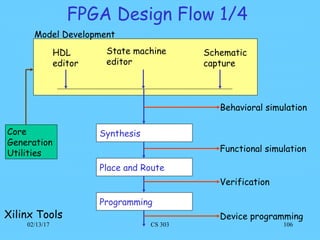
  • 102. 106 FPGA Design Flow 1/4 HDL editor State machine editor Schematic capture Synthesis Place and Route Programming Behavioral simulation Functional simulation Verification Device programmingXilinx Tools Core Generation Utilities Model Development 02/13/17 CS 303
  • 103. 107 FPGA Design Flow 2/4 • Model development: – VHDL code – State-machines may be described in a graphical manner and translated into VHDL code. – Traditional schematic capture can be translated into VHDL source. • Behavioral Simulation – Before synthesis; for testing functional correctness • Synthesis – The design is synthesized to a library of primitive components such as gates, flip-flops, and latches • Functional Simulation – To find out preliminary performance estimates – For example, timing information can be obtained from known properties of FPGA components – Still not too accurate 02/13/17 CS 303
  • 104. 108 FPGA Design Flow 3/4 • Place and Route: – The design is mapped to the primitives in the target chip – In FPGA, there are function generators (LUTs), flip- flops, and latches – Each primitive must be assigned to a specific CLB (Placement) – Connections between CLBs that implement the primitives must be established (routing) – Accurate timing can be obtained in Verification step (Post-placement and routing simulation) – The configuration bits are generated. 02/13/17 CS 303
  • 105. 109 FPGA Design Flow 4/4 • Programming: – The configuration data (bit stream) is finally loaded into the target FPGA chip. • These steps are fairly generic although the terminology used here is adopted from Xilinx. 02/13/17 CS 303
  • 106. 110 Xilinx Tools: Design Flow 02/13/17 CS 303