SlideShare a Scribd company logo
RESISTIVITY
Roll. No. 17MSE006 , 17MSE011 , 17MSE012 , 17MSE017
MTech Student, SSE PDPU
OUTLINE
• To understand the concept of resistivity
• Resistivity measurement technique
• Sheet resistance
• Measurement Errors and precautions
• Wafer Mapping
• Contactless resistivity measurement technique
• Strength and weaknesses of Various measurement
techniques
• Conclusion
 TO UNDERSTAND THE CONCEPT OF
RESISTIVITY
• Measure of the resisting power of a specified material to the flow of an electric
current.
• Resistivity is commonly represented by the Greek letter ρ (rho).
• The SI unit of electrical resistivity is the ohm-meter (Ω⋅m)
• Resistivity ρ=R(A/L)
Material Resistivity, ρ (Ω·m)
Superconductors 0
Metals 10−8
Semiconductors Variable
Electrolytes Variable
Insulators 1016
Super insulators ∞
Resistivity
Measurement
Technique
Two point probe
method
Four point probe
method
1.TWO POINT PROBE METHOD
 Basically a two point contact
 Each contact serves as a current and as a voltage probe
 Appear to be easier but the interpretation of the measured data is
difficult due to various resistance inclusion
Rw
V
Rw
Rc
Rc
RDUT
DUT
RT = V/I= 2RW + 2RC + RDUT
2.FOUR POINT PROBE METHOD
Originally proposed by wenner to
measure the resistivity of the earth
Later, Adopted for semiconductor
wafer as well and widely used in
wafer manufacturing industries
V
Rw
Rc
Rc
RDUT
DUT
WHY FOUR POINT PROBE?
• To attain the standardization of Probe technique with utmost accuracy
• Current path is same as that of the two probe method
• But, Voltage is measured with two additional contact
• Input impedance of voltmeter around 1012 ohms or higher so current
not large amount pass in voltmeter.
• the voltage drops across RW and RC are negligibly small and can be
neglected and the measured voltage is essentially the voltage drop
across the DUT
• The four point probe method, as indicated in Figure, has four equally spaced in-line probes with
probe tip diameters small compared to the probe spacing, S.
Depletion region act as an insulator
Keep current flow in the emitter
V
N
P
t
S S S
Current source and measurement
• Current is most commonly passed between the outer two probes, and
the voltage difference is measured between the two inner probes.
Resistivity in a four-point probe measurement is given by
𝜌 = 2𝜋𝑠𝐹
𝑉
𝐼
• Where
s is the distance between two probe
F represents the correction factor
• F = F1 F2 F3
• F1 corrects for sample thickness,
• F2 for lateral sample dimensions,
• F3 for placement of the probes relative to the sample edges.
EXPERIMENTAL PROCEDURE:
Source.: F.M.Smits, "Measurement of Sheet Resistivities with the Four-Point Probe", The Bell System
Technical Journal 37, 711-718
Reference: RESISTIVITY OF A SEMICONDUCTOR BY THE FOUR-PROBE METHOD (Dr Jeethendra Kumar P K)
Let a Sample n-type Germanium Semiconductor
Dimensions : (L) 2mm x (d) 5.4mm x (t) 0.5mm
Probe Spacing (S) : 2mm
 Resistivity for equally spaced probes is given
by
𝜌 = 2𝜋𝑠𝐹
𝑉
𝐼
 Calculating ratios “t/S” and “d/S”
t/S = 0.25 ; d/S = 2.7
𝜌 = 4.53𝑡 × 𝐹 ×
𝑉
𝐼
It is observed by experimentation that the sample with thickness-gap
ratio t/S≤0.5, the geometric factor 2πS is given by
2πS =
𝜋
𝑙𝑛2
× 𝑡 =4.53t
 Hence for a finite width and non-negligible thickness is
given by:
𝐹 = 𝑓1 𝑓2
Where 𝑓1 & 𝑓2 are determined from the graph
𝑓1 = 1 ; 𝑓2 = 0.59
𝜌 = 1.33 × 10⁻³ ×
𝑉
𝐼
 The sample is placed under the four probes such that the probes are
parallel to the longer side (length) of the sample.
Reference: RESISTIVITY OF A SEMICONDUCTOR BY THE FOUR-PROBE METHOD (Dr Jeethendra Kumar P K)
 The current is set to 0.1mA by adjusting set-current knob. The voltage
developed across the inner probes is noted
Current (mA)
Sample-1
mV V/I
0.1 5.4 54.0
0.2 10.5 52.5
0.3 16.0 53.3
0.4 21.1 52.7
0.5 26.5 53.0
0.6 31.7 52.8
0.7 37.0 52.8
0.8 42.3 53.3
0.9 48.0 53.0
1.0 53.0 53.0
1.1 58.3 53.0
1.2 63.5 52.9
1.3 69.0 53.0
1.4 74.4 53.1
1.5 79.8 53.2
Average V/I 53.0
𝜌 = 1.33 × 10−3
× 53
= 0.0708 𝛺 − 𝑚
= 7.08 𝛺 − 𝑐𝑚
SHEET RESISTANCE
• Measure of the resistivity averaged over the
surface
• Sheet resistance is a measure of resistance of
thin films that are nominally uniform in
thickness.
• The utility of sheet resistance as opposed
to resistance or resistivity is that it is directly
measured using a four-point probe
measurement or indirectly by using a non-
contact eddy current based testing device.
• Sheet resistance can be used to compare the
electrical properties of devices that are
significantly different in size.
𝑅 = 𝑅 𝑠ℎ
𝐿
𝑊
ohms
𝑅 = 𝜌
𝐿
𝐴
= 𝜌
𝐿
𝑊𝑡
=
𝜌
𝑡
𝐿
𝑊
Ohms
CONTD.
• Since
𝐿
𝑊
has no units,
𝜌
𝑡
should have units of ohms. But
𝜌
𝑡
is not the sample
resistance.
• To distinguish between R and
𝜌
𝑡
, Often in practice, surface resistivity is given in
units of
Ω
𝑆𝑞𝑢𝑎𝑟𝑒
• Sheet resistance is applicable as long as the measurement is related to a square.
Minority Majority
(carrier injection)
Probe spacing
CurrentSample Size
High Resistivity
Materials
FACTORS AFFECTING THE MEASUREMENT ACCURACY
Measurement
Errors and
Precautions
SAMPLE SIZE
• correction factor F depends on the thickness of the material
• If the wafer or the layer to be measured is appreciably thinner than the probe spacing,
the calculated resistivity varies directly with thickness.
• It is therefore very important to determine the thickness accurately for resistivity
determination.
MINORITY - MAJORITY CARRIER INJECTION
• Metal-semiconductor contacts do inject minority carriers, but their injection efficiency is
low.
• However, under high current conditions it may not be negligible.
• Minority carrier injection causes conductivity modulation because increased minority
carrier density leads to increased majority carrier density (to maintain charge neutrality)
and subsequent enhanced conductivity.
• To reduce minority carrier injection, the surface should have a high recombination rate for
minority carriers. This is best achieved by using lapped surfaces.
PROBE SPACING
• A mechanical four-point probe exhibits small random probe spacing
variations.
• Such variations give erroneous values of resistivity or sheet resistance,
especially when evaluating uniformly doped wafers.
• In such cases it is very important to know whether any non-uniformities are
due to the wafer, due to process variations, or due to measurement errors.
CURRENT
• The current can affect the
measured resistivity in two ways:
1. by an apparent resistivity increase
produced by wafer heating
2. by an apparent resistivity
decrease due to minority and/or
majority carrier injection.
10−2
10−1
100
101
102
103
10−2
10−1
100
101
102
103
104
Current (mA)
Resistivity(Ω-cm)
SheetResistance(Ω-
Square)
HIGH RESISTIVITY MATERIALS
• Materials of very high resistivity are more difficult to measure by four-point probe method.
• Moderately doped wafers can become highly resistive at low temperatures and are similarly
difficult to measure.
WAFER MAPPING
• originated in the 1970s
• originally developed to characterize ion implantation uniformity
• During wafer mapping the sheet resistance or some other parameter
proportional to ion implant dose is measured at many locations across a
sample. The data are then converted to two-dimensional or three-
dimensional contour maps
• Contour maps are a more powerful display of process uniformity than
displaying the same data in tabular form. A well-designed contour map gives
instant information about ion implant uniformity, flow patterns during
diffusion, epitaxial reactor non-uniformities, etc.
THE MOST COMMON SHEET RESISTANCE WAFER
MAPPING TECHNIQUES ARE:
Wafer mapping techniques
Double implant
technique
Modulated
photoreflectance
Optical
densitometry
DOUBLE IMPLANT TECHNIQUE
A p-type (n-type) impurity is implanted into an n-type (p-type) substrate at a dose 1 and energy
E1.
desired low-dose impurity is implanted at dose 2 and energy E2, with E2 < E1.
E2 should be less than E1 to prevent penetration through the first implant layer.
The sheet resistance Rsh2 after the second implant is
measured and compared to Rsh1 without annealing the
second implant.
The second sheet resistance measurement relies on the
implant damage of the second implant being proportional to
the implant dose.
Four-point probe sheet resistance
Four- point prob contour map
(A) Boron, 1015
𝑐𝑚−2
, 40 keV, Rsh (average) = 98.5 ohms/square
(B) (B) Arsenic, 1015 𝑐𝑚−2 , 80 keV, Rsh (average) = 98.5 ohms/square
1% intervals, 200 mm diameter Si wafer
A B
MODULATED PHOTO REFLECTANCE
In the modulated photo reflectance ,an Ar+ ion laser beam, incident on the semiconductor sample, is
modulated at a frequency of 0.1 to 10 MHz, creating transient thermal waves near the surface that
propagate at different speeds in damaged and crystalline regions.
Hence, signals from regions with various damages differ, leading to a measure of crystal damage.
The thermal wave diffusion length at a 1 MHz modulation frequency is 2 to 3 μm.
The small temperature variations cause small volume changes of the wafer near the surface and the
surface expands slightly.
These changes include both thermoelastic and optical effects, and they are detected with a second
laser—the probe beam—by measuring the reflectivity change
• The technique is contactless and non-destructive and has been used to measure
implant doses from 10^11 to 10^15 cm^3
• Its chief strength lies in the ability to detect low-dose implants contactless and to
display the information as contour maps.
Damaged layer
Therma
l signal
Pump
laser
Sample
Detector
Prob
laser
Modulated photoreflectance contour map
(A) Boron, 6.5*1012
𝑐𝑚−2
, 70 keV, 648 TW units
(B) Boron, 5*1012
𝑐𝑚−2
, 30 keV, 600 TW units
0.5% intervals, 200 mm diameter Si wafer
A B
OPTICAL DENSITOMETRY
A transparent substrate, typically glass, is coated with a thin
film consisting of a polymer carrier and an implant sensitive
radiochromic dye.
During implant, the dye molecule undergoes heterolytic
cleavage, resulting in positive ions with a peak light
absorption at a wavelength of 600 nm.
When this polymer-coated glass wafer is ion implanted, the
film darkens. The amount of darkening depends on the
implant energy, dose, and species.
COMPARISON OF VARIOUS MEASUREMENT TECHNIQUES
Category
Four Point
Probe
Double Implant
Spreading
Resistance
Modulated
Photoreflectan
e
Optical
Densitometry
Type Electrical Electrical Electrical Optical Optical
Measurement Sheet Resistance Crystal Damage
Spreading
Resistance
Crystal Damage
Polymer
Damage
Resolution(µm) 3000 3000 5 1 3000
Species Active Active Active , Inactive Inactive Inactive
Dose
Range(𝑐𝑚−2
)
1012 - 1015 1011 - 1014
1011 - 1015 1011 - 1015 1011 - 1013
Results Direct Calibration Calibration Calibration Calibration
Relaxation Minor Serious Minor Serious Serious
Requires Anneal Initial Implant Anneal
_______ Measure before
and after
Mapping Techniques for Ion Implantation Uniformity
Measurements
CONTACTLESS RESISTIVITY MEASUREMENT TECHNIQUE
Contactless resistivity
measurement technique
electrical
the sample is placed into a microwave circuit and
get the transmission or reflection
characteristics of a waveguide or cavity,
the sample is capacitively coupled to the
measuring apparatus
the sample is inductively coupled to the
apparatus
Non-electrical
ONE SUCH CONTACTLESS TECHNIQUE IS EDDY CURRENT TECHNIQUE
• The eddy current measurement technique is based on the parallel resonant tank circuit.
• The quality factor of such a circuit is reduced when a conducting material is brought close to the coil due to
the power absorbed by the conducting material.
• In the ultrasound method sound waves are reflected from the
upper and lower wafer surfaces located between the two probes .
• The phase shift of the reflected sound caused by the impedance
variation of the air gap is detected by the sonic receiver.
• The phase shift is proportional to the distance from each probe to
each surface. With known probe spacing, the wafer thickness can be
determined.
STRENGTH AND WEAKNESSES OF VARIOUS
RESISTIVITY MEASUREMENT TECHNIQUE
FOUR-POINT PROBE TECHNIQUE
Strength Weakness
absolute measurement without
recourse to calibrated standards
surface damage
wafer mapping makes it powerful
monitoring tool
samples a relatively large volume
of the wafer, prevents high
resolution measurements
CONTACTLESS TECHNIQUES
Strength Weakness
non-contacting nature prevents
destruction of material
inability to determine the sheet
resistance of thin diffused or ion-
implanted layers
availability of commercial equipment Need of highly doped layer on an
insulating substrate to detect such
resistance by making sheet
resistance of the layer to be on the
order of a hundred times lower than
the sheet resistance of the substrate
OPTICAL TECHNIQUES
Strength Weakness
Ability to measure the implants non-
destructively, with small spot size
Measurements are qualitative with
quantitative doping requires calibrated
standards
Rapid technique compared to others Possible laser drift
Displaying the information in the form
of contour plots
Al backing plate must be affixed to
protect optical sensors
EFFECT OF PRESSURE ON RESISTIVITY OF
SEMICONDUCTORS:
Amorphous Silicon
• Effects of hydrostatic pressure on
electrical resistively of Amorphous
Silicon at room temperature have been
experimentally investigated and
plotted in the graph as shown
Selenium
• Selenium is other group material with a direct band gap in
type conduction. It is used in selenium rectifiers.
• The effects of pressure on the optical edge of selenium have
been studied by Balchan and Drickamer
GermaniumSelenium
RESISTIVITY OF VARIOUS MATERIALS
Material Resistivity at 23º C
Ohms - meter
Material Resistivity at 23º C
Ohms - meter
Silver 1.59 𝑥10−8 Nichrome 1.50 𝑥10−6
Copper 1.68 𝑥10−8 Coal 3.5 𝑥10−5
Gold 2.20 𝑥10−8 Germanium 4.6 𝑥10−1
Aluminum 2.65 𝑥10−8 Silicon 6.4 𝑥102
Tungsten 5.6 𝑥10−8 Human Skin 5 𝑥105
Iron 9.71 𝑥10−8 Glass 101
𝑡𝑜 1014
Steel 7.2 𝑥10−7 Rubber 1013
Platinum 1.1 𝑥10−7 Sulfur 1015
Lead 2.2 𝑥10−7 Quartz 7.5 𝑥1017
• Reference:
1. Semiconductor Material And Device Characterization By Dieter K.
Schroder
2. Electrical resistivity/ resistance of some semiconductors by Rajendra
Kumar and Tanveer Ahmad Wani

More Related Content

PPT
Plasma Etching
PPTX
Reactive ion etching (RIE)
PDF
Thin film and thick film resistor
PPT
Introduction to thin film growth and molecular beam epitaxy
PPTX
Oxidation
PPTX
Thin films and chemical bath deposition technique
PPTX
Ion beam etching (or) Ion milling
PPTX
Oxidation--ABU SYED KUET
Plasma Etching
Reactive ion etching (RIE)
Thin film and thick film resistor
Introduction to thin film growth and molecular beam epitaxy
Oxidation
Thin films and chemical bath deposition technique
Ion beam etching (or) Ion milling
Oxidation--ABU SYED KUET

What's hot (20)

PPTX
PDF
IC Fabrication Process
PDF
High k dielectrics
PPTX
PPTX
Silicon on Insulator (SOI) Technology
PPTX
Introduction to FINFET, Details of FinFET
PPTX
Lightly Doped Drain
PPT
Soliton
PPT
Chapter3
PPTX
Ion implantation
PPTX
Introduction to FinFET
PPTX
Vapor Phase Deposition Techniques
PDF
Engineering physics 5(Quantum free electron theory)
PDF
Metal Semi-Conductor Junctions
PPT
MOSFET Small signal model
PPT
Opto electronics devices
PPTX
EC6202 ELECTRONIC DEVICES AND CIRCUITS Unit 1
PDF
Analog Layout design
PPT
Microstrip Patch Antenna Design
IC Fabrication Process
High k dielectrics
Silicon on Insulator (SOI) Technology
Introduction to FINFET, Details of FinFET
Lightly Doped Drain
Soliton
Chapter3
Ion implantation
Introduction to FinFET
Vapor Phase Deposition Techniques
Engineering physics 5(Quantum free electron theory)
Metal Semi-Conductor Junctions
MOSFET Small signal model
Opto electronics devices
EC6202 ELECTRONIC DEVICES AND CIRCUITS Unit 1
Analog Layout design
Microstrip Patch Antenna Design
Ad

Similar to sheet resistivity (20)

PDF
Four probe-method
PPT
For Four Point Probe Technique.ppt for best
PPTX
Junction-depth & Sheet-resitance meassurement
PPT
Electrical measurements and two probe method
PPTX
Four probe Method.pptx
PDF
4 pointprobe manual
PPTX
Report on diffusion
PPTX
Resistivity of semiconductor by four probe method.pptx
PPTX
Characterization Techniques for Electronic Devices.pptx
PDF
sheet-resistance-measurement
PDF
Resistivity Survey
PPTX
conventional resistivity logs
PDF
Assignment Presentation Final
PPTX
general physics laboratory experiments lab
PDF
Sheet Resistance Measurement by EddyCus TF lab 2020
PDF
Sheet Resistance Measurement by EddyCus TF lab 4040
PDF
Sheet Resistance Mapping of Functional Thin-Film by EddyCus TF map 4040SR
PDF
Microwave Planar Sensor for Determination of the Permittivity of Dielectric M...
PPT
Resistivity method
PPT
Nondestructive Approach to Evaluate Defects in Elements of Agricultural Machi...
Four probe-method
For Four Point Probe Technique.ppt for best
Junction-depth & Sheet-resitance meassurement
Electrical measurements and two probe method
Four probe Method.pptx
4 pointprobe manual
Report on diffusion
Resistivity of semiconductor by four probe method.pptx
Characterization Techniques for Electronic Devices.pptx
sheet-resistance-measurement
Resistivity Survey
conventional resistivity logs
Assignment Presentation Final
general physics laboratory experiments lab
Sheet Resistance Measurement by EddyCus TF lab 2020
Sheet Resistance Measurement by EddyCus TF lab 4040
Sheet Resistance Mapping of Functional Thin-Film by EddyCus TF map 4040SR
Microwave Planar Sensor for Determination of the Permittivity of Dielectric M...
Resistivity method
Nondestructive Approach to Evaluate Defects in Elements of Agricultural Machi...
Ad

More from paneliya sagar (20)

PPTX
Energy efficint colling
PPTX
Thermodynamic properties, processes and cycles
PPTX
The first law of thermodynamics
PPTX
Second law of thermodynamics
PPTX
first law of thermodynamics
PPTX
available energy ,irreversibility,exchargy
PPTX
Carnot theorem
PPTX
equivalency and irreversibility
PPTX
intro to thermodynamics
PPTX
Electron beam lithography
PPTX
solar cell characteristics
PPTX
schottky barrier and contact resistance
PPTX
carrier and doping density
PPTX
Characterization of Carrier Lifetime
PPTX
17 mse018 solar hybrid system
PPTX
17 mse017 battery and battery management system
PPTX
17 mse016 solar pv pumping
PDF
17 mse014 pv syst
PPTX
17 mse013 performance of power plant
PPTX
17 mse012 solar tracking system
Energy efficint colling
Thermodynamic properties, processes and cycles
The first law of thermodynamics
Second law of thermodynamics
first law of thermodynamics
available energy ,irreversibility,exchargy
Carnot theorem
equivalency and irreversibility
intro to thermodynamics
Electron beam lithography
solar cell characteristics
schottky barrier and contact resistance
carrier and doping density
Characterization of Carrier Lifetime
17 mse018 solar hybrid system
17 mse017 battery and battery management system
17 mse016 solar pv pumping
17 mse014 pv syst
17 mse013 performance of power plant
17 mse012 solar tracking system

Recently uploaded (20)

PPTX
CHAPTER IV. MAN AND BIOSPHERE AND ITS TOTALITY.pptx
PPTX
B.Sc. DS Unit 2 Software Engineering.pptx
PDF
Hazard Identification & Risk Assessment .pdf
PPTX
20th Century Theater, Methods, History.pptx
PPTX
Chinmaya Tiranga Azadi Quiz (Class 7-8 )
PDF
HVAC Specification 2024 according to central public works department
PDF
Practical Manual AGRO-233 Principles and Practices of Natural Farming
PDF
Weekly quiz Compilation Jan -July 25.pdf
PPTX
202450812 BayCHI UCSC-SV 20250812 v17.pptx
PPTX
History, Philosophy and sociology of education (1).pptx
PDF
1.3 FINAL REVISED K-10 PE and Health CG 2023 Grades 4-10 (1).pdf
PDF
Empowerment Technology for Senior High School Guide
PPTX
Introduction to pro and eukaryotes and differences.pptx
PDF
Paper A Mock Exam 9_ Attempt review.pdf.
PDF
A GUIDE TO GENETICS FOR UNDERGRADUATE MEDICAL STUDENTS
PDF
IGGE1 Understanding the Self1234567891011
PDF
RTP_AR_KS1_Tutor's Guide_English [FOR REPRODUCTION].pdf
PPTX
Computer Architecture Input Output Memory.pptx
PDF
medical_surgical_nursing_10th_edition_ignatavicius_TEST_BANK_pdf.pdf
PDF
AI-driven educational solutions for real-life interventions in the Philippine...
CHAPTER IV. MAN AND BIOSPHERE AND ITS TOTALITY.pptx
B.Sc. DS Unit 2 Software Engineering.pptx
Hazard Identification & Risk Assessment .pdf
20th Century Theater, Methods, History.pptx
Chinmaya Tiranga Azadi Quiz (Class 7-8 )
HVAC Specification 2024 according to central public works department
Practical Manual AGRO-233 Principles and Practices of Natural Farming
Weekly quiz Compilation Jan -July 25.pdf
202450812 BayCHI UCSC-SV 20250812 v17.pptx
History, Philosophy and sociology of education (1).pptx
1.3 FINAL REVISED K-10 PE and Health CG 2023 Grades 4-10 (1).pdf
Empowerment Technology for Senior High School Guide
Introduction to pro and eukaryotes and differences.pptx
Paper A Mock Exam 9_ Attempt review.pdf.
A GUIDE TO GENETICS FOR UNDERGRADUATE MEDICAL STUDENTS
IGGE1 Understanding the Self1234567891011
RTP_AR_KS1_Tutor's Guide_English [FOR REPRODUCTION].pdf
Computer Architecture Input Output Memory.pptx
medical_surgical_nursing_10th_edition_ignatavicius_TEST_BANK_pdf.pdf
AI-driven educational solutions for real-life interventions in the Philippine...

sheet resistivity

  • 1. RESISTIVITY Roll. No. 17MSE006 , 17MSE011 , 17MSE012 , 17MSE017 MTech Student, SSE PDPU
  • 2. OUTLINE • To understand the concept of resistivity • Resistivity measurement technique • Sheet resistance • Measurement Errors and precautions • Wafer Mapping • Contactless resistivity measurement technique • Strength and weaknesses of Various measurement techniques • Conclusion
  • 3.  TO UNDERSTAND THE CONCEPT OF RESISTIVITY • Measure of the resisting power of a specified material to the flow of an electric current. • Resistivity is commonly represented by the Greek letter ρ (rho). • The SI unit of electrical resistivity is the ohm-meter (Ω⋅m) • Resistivity ρ=R(A/L) Material Resistivity, ρ (Ω·m) Superconductors 0 Metals 10−8 Semiconductors Variable Electrolytes Variable Insulators 1016 Super insulators ∞
  • 5. 1.TWO POINT PROBE METHOD  Basically a two point contact  Each contact serves as a current and as a voltage probe  Appear to be easier but the interpretation of the measured data is difficult due to various resistance inclusion Rw V Rw Rc Rc RDUT DUT RT = V/I= 2RW + 2RC + RDUT
  • 6. 2.FOUR POINT PROBE METHOD Originally proposed by wenner to measure the resistivity of the earth Later, Adopted for semiconductor wafer as well and widely used in wafer manufacturing industries V Rw Rc Rc RDUT DUT
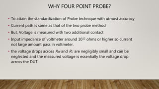
  • 7. WHY FOUR POINT PROBE? • To attain the standardization of Probe technique with utmost accuracy • Current path is same as that of the two probe method • But, Voltage is measured with two additional contact • Input impedance of voltmeter around 1012 ohms or higher so current not large amount pass in voltmeter. • the voltage drops across RW and RC are negligibly small and can be neglected and the measured voltage is essentially the voltage drop across the DUT
  • 8. • The four point probe method, as indicated in Figure, has four equally spaced in-line probes with probe tip diameters small compared to the probe spacing, S. Depletion region act as an insulator Keep current flow in the emitter V N P t S S S Current source and measurement
  • 9. • Current is most commonly passed between the outer two probes, and the voltage difference is measured between the two inner probes. Resistivity in a four-point probe measurement is given by 𝜌 = 2𝜋𝑠𝐹 𝑉 𝐼 • Where s is the distance between two probe F represents the correction factor • F = F1 F2 F3 • F1 corrects for sample thickness, • F2 for lateral sample dimensions, • F3 for placement of the probes relative to the sample edges.
  • 10. EXPERIMENTAL PROCEDURE: Source.: F.M.Smits, "Measurement of Sheet Resistivities with the Four-Point Probe", The Bell System Technical Journal 37, 711-718 Reference: RESISTIVITY OF A SEMICONDUCTOR BY THE FOUR-PROBE METHOD (Dr Jeethendra Kumar P K) Let a Sample n-type Germanium Semiconductor Dimensions : (L) 2mm x (d) 5.4mm x (t) 0.5mm Probe Spacing (S) : 2mm  Resistivity for equally spaced probes is given by 𝜌 = 2𝜋𝑠𝐹 𝑉 𝐼  Calculating ratios “t/S” and “d/S” t/S = 0.25 ; d/S = 2.7 𝜌 = 4.53𝑡 × 𝐹 × 𝑉 𝐼 It is observed by experimentation that the sample with thickness-gap ratio t/S≤0.5, the geometric factor 2πS is given by 2πS = 𝜋 𝑙𝑛2 × 𝑡 =4.53t  Hence for a finite width and non-negligible thickness is given by: 𝐹 = 𝑓1 𝑓2 Where 𝑓1 & 𝑓2 are determined from the graph 𝑓1 = 1 ; 𝑓2 = 0.59 𝜌 = 1.33 × 10⁻³ × 𝑉 𝐼
  • 11.  The sample is placed under the four probes such that the probes are parallel to the longer side (length) of the sample. Reference: RESISTIVITY OF A SEMICONDUCTOR BY THE FOUR-PROBE METHOD (Dr Jeethendra Kumar P K)  The current is set to 0.1mA by adjusting set-current knob. The voltage developed across the inner probes is noted Current (mA) Sample-1 mV V/I 0.1 5.4 54.0 0.2 10.5 52.5 0.3 16.0 53.3 0.4 21.1 52.7 0.5 26.5 53.0 0.6 31.7 52.8 0.7 37.0 52.8 0.8 42.3 53.3 0.9 48.0 53.0 1.0 53.0 53.0 1.1 58.3 53.0 1.2 63.5 52.9 1.3 69.0 53.0 1.4 74.4 53.1 1.5 79.8 53.2 Average V/I 53.0 𝜌 = 1.33 × 10−3 × 53 = 0.0708 𝛺 − 𝑚 = 7.08 𝛺 − 𝑐𝑚
  • 12. SHEET RESISTANCE • Measure of the resistivity averaged over the surface • Sheet resistance is a measure of resistance of thin films that are nominally uniform in thickness. • The utility of sheet resistance as opposed to resistance or resistivity is that it is directly measured using a four-point probe measurement or indirectly by using a non- contact eddy current based testing device. • Sheet resistance can be used to compare the electrical properties of devices that are significantly different in size. 𝑅 = 𝑅 𝑠ℎ 𝐿 𝑊 ohms 𝑅 = 𝜌 𝐿 𝐴 = 𝜌 𝐿 𝑊𝑡 = 𝜌 𝑡 𝐿 𝑊 Ohms
  • 13. CONTD. • Since 𝐿 𝑊 has no units, 𝜌 𝑡 should have units of ohms. But 𝜌 𝑡 is not the sample resistance. • To distinguish between R and 𝜌 𝑡 , Often in practice, surface resistivity is given in units of Ω 𝑆𝑞𝑢𝑎𝑟𝑒 • Sheet resistance is applicable as long as the measurement is related to a square.
  • 14. Minority Majority (carrier injection) Probe spacing CurrentSample Size High Resistivity Materials FACTORS AFFECTING THE MEASUREMENT ACCURACY Measurement Errors and Precautions
  • 15. SAMPLE SIZE • correction factor F depends on the thickness of the material • If the wafer or the layer to be measured is appreciably thinner than the probe spacing, the calculated resistivity varies directly with thickness. • It is therefore very important to determine the thickness accurately for resistivity determination.
  • 16. MINORITY - MAJORITY CARRIER INJECTION • Metal-semiconductor contacts do inject minority carriers, but their injection efficiency is low. • However, under high current conditions it may not be negligible. • Minority carrier injection causes conductivity modulation because increased minority carrier density leads to increased majority carrier density (to maintain charge neutrality) and subsequent enhanced conductivity. • To reduce minority carrier injection, the surface should have a high recombination rate for minority carriers. This is best achieved by using lapped surfaces.
  • 17. PROBE SPACING • A mechanical four-point probe exhibits small random probe spacing variations. • Such variations give erroneous values of resistivity or sheet resistance, especially when evaluating uniformly doped wafers. • In such cases it is very important to know whether any non-uniformities are due to the wafer, due to process variations, or due to measurement errors.
  • 18. CURRENT • The current can affect the measured resistivity in two ways: 1. by an apparent resistivity increase produced by wafer heating 2. by an apparent resistivity decrease due to minority and/or majority carrier injection. 10−2 10−1 100 101 102 103 10−2 10−1 100 101 102 103 104 Current (mA) Resistivity(Ω-cm) SheetResistance(Ω- Square)
  • 19. HIGH RESISTIVITY MATERIALS • Materials of very high resistivity are more difficult to measure by four-point probe method. • Moderately doped wafers can become highly resistive at low temperatures and are similarly difficult to measure.
  • 20. WAFER MAPPING • originated in the 1970s • originally developed to characterize ion implantation uniformity • During wafer mapping the sheet resistance or some other parameter proportional to ion implant dose is measured at many locations across a sample. The data are then converted to two-dimensional or three- dimensional contour maps • Contour maps are a more powerful display of process uniformity than displaying the same data in tabular form. A well-designed contour map gives instant information about ion implant uniformity, flow patterns during diffusion, epitaxial reactor non-uniformities, etc.
  • 21. THE MOST COMMON SHEET RESISTANCE WAFER MAPPING TECHNIQUES ARE: Wafer mapping techniques Double implant technique Modulated photoreflectance Optical densitometry
  • 22. DOUBLE IMPLANT TECHNIQUE A p-type (n-type) impurity is implanted into an n-type (p-type) substrate at a dose 1 and energy E1. desired low-dose impurity is implanted at dose 2 and energy E2, with E2 < E1. E2 should be less than E1 to prevent penetration through the first implant layer. The sheet resistance Rsh2 after the second implant is measured and compared to Rsh1 without annealing the second implant. The second sheet resistance measurement relies on the implant damage of the second implant being proportional to the implant dose.
  • 23. Four-point probe sheet resistance Four- point prob contour map (A) Boron, 1015 𝑐𝑚−2 , 40 keV, Rsh (average) = 98.5 ohms/square (B) (B) Arsenic, 1015 𝑐𝑚−2 , 80 keV, Rsh (average) = 98.5 ohms/square 1% intervals, 200 mm diameter Si wafer A B
  • 24. MODULATED PHOTO REFLECTANCE In the modulated photo reflectance ,an Ar+ ion laser beam, incident on the semiconductor sample, is modulated at a frequency of 0.1 to 10 MHz, creating transient thermal waves near the surface that propagate at different speeds in damaged and crystalline regions. Hence, signals from regions with various damages differ, leading to a measure of crystal damage. The thermal wave diffusion length at a 1 MHz modulation frequency is 2 to 3 μm. The small temperature variations cause small volume changes of the wafer near the surface and the surface expands slightly. These changes include both thermoelastic and optical effects, and they are detected with a second laser—the probe beam—by measuring the reflectivity change
  • 25. • The technique is contactless and non-destructive and has been used to measure implant doses from 10^11 to 10^15 cm^3 • Its chief strength lies in the ability to detect low-dose implants contactless and to display the information as contour maps. Damaged layer Therma l signal Pump laser Sample Detector Prob laser Modulated photoreflectance contour map (A) Boron, 6.5*1012 𝑐𝑚−2 , 70 keV, 648 TW units (B) Boron, 5*1012 𝑐𝑚−2 , 30 keV, 600 TW units 0.5% intervals, 200 mm diameter Si wafer A B
  • 26. OPTICAL DENSITOMETRY A transparent substrate, typically glass, is coated with a thin film consisting of a polymer carrier and an implant sensitive radiochromic dye. During implant, the dye molecule undergoes heterolytic cleavage, resulting in positive ions with a peak light absorption at a wavelength of 600 nm. When this polymer-coated glass wafer is ion implanted, the film darkens. The amount of darkening depends on the implant energy, dose, and species.
  • 27. COMPARISON OF VARIOUS MEASUREMENT TECHNIQUES Category Four Point Probe Double Implant Spreading Resistance Modulated Photoreflectan e Optical Densitometry Type Electrical Electrical Electrical Optical Optical Measurement Sheet Resistance Crystal Damage Spreading Resistance Crystal Damage Polymer Damage Resolution(µm) 3000 3000 5 1 3000 Species Active Active Active , Inactive Inactive Inactive Dose Range(𝑐𝑚−2 ) 1012 - 1015 1011 - 1014 1011 - 1015 1011 - 1015 1011 - 1013 Results Direct Calibration Calibration Calibration Calibration Relaxation Minor Serious Minor Serious Serious Requires Anneal Initial Implant Anneal _______ Measure before and after Mapping Techniques for Ion Implantation Uniformity Measurements
  • 28. CONTACTLESS RESISTIVITY MEASUREMENT TECHNIQUE Contactless resistivity measurement technique electrical the sample is placed into a microwave circuit and get the transmission or reflection characteristics of a waveguide or cavity, the sample is capacitively coupled to the measuring apparatus the sample is inductively coupled to the apparatus Non-electrical
  • 29. ONE SUCH CONTACTLESS TECHNIQUE IS EDDY CURRENT TECHNIQUE • The eddy current measurement technique is based on the parallel resonant tank circuit. • The quality factor of such a circuit is reduced when a conducting material is brought close to the coil due to the power absorbed by the conducting material.
  • 30. • In the ultrasound method sound waves are reflected from the upper and lower wafer surfaces located between the two probes . • The phase shift of the reflected sound caused by the impedance variation of the air gap is detected by the sonic receiver. • The phase shift is proportional to the distance from each probe to each surface. With known probe spacing, the wafer thickness can be determined.
  • 31. STRENGTH AND WEAKNESSES OF VARIOUS RESISTIVITY MEASUREMENT TECHNIQUE
  • 32. FOUR-POINT PROBE TECHNIQUE Strength Weakness absolute measurement without recourse to calibrated standards surface damage wafer mapping makes it powerful monitoring tool samples a relatively large volume of the wafer, prevents high resolution measurements
  • 33. CONTACTLESS TECHNIQUES Strength Weakness non-contacting nature prevents destruction of material inability to determine the sheet resistance of thin diffused or ion- implanted layers availability of commercial equipment Need of highly doped layer on an insulating substrate to detect such resistance by making sheet resistance of the layer to be on the order of a hundred times lower than the sheet resistance of the substrate
  • 34. OPTICAL TECHNIQUES Strength Weakness Ability to measure the implants non- destructively, with small spot size Measurements are qualitative with quantitative doping requires calibrated standards Rapid technique compared to others Possible laser drift Displaying the information in the form of contour plots Al backing plate must be affixed to protect optical sensors
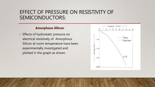
  • 35. EFFECT OF PRESSURE ON RESISTIVITY OF SEMICONDUCTORS: Amorphous Silicon • Effects of hydrostatic pressure on electrical resistively of Amorphous Silicon at room temperature have been experimentally investigated and plotted in the graph as shown
  • 36. Selenium • Selenium is other group material with a direct band gap in type conduction. It is used in selenium rectifiers. • The effects of pressure on the optical edge of selenium have been studied by Balchan and Drickamer GermaniumSelenium
  • 37. RESISTIVITY OF VARIOUS MATERIALS Material Resistivity at 23º C Ohms - meter Material Resistivity at 23º C Ohms - meter Silver 1.59 𝑥10−8 Nichrome 1.50 𝑥10−6 Copper 1.68 𝑥10−8 Coal 3.5 𝑥10−5 Gold 2.20 𝑥10−8 Germanium 4.6 𝑥10−1 Aluminum 2.65 𝑥10−8 Silicon 6.4 𝑥102 Tungsten 5.6 𝑥10−8 Human Skin 5 𝑥105 Iron 9.71 𝑥10−8 Glass 101 𝑡𝑜 1014 Steel 7.2 𝑥10−7 Rubber 1013 Platinum 1.1 𝑥10−7 Sulfur 1015 Lead 2.2 𝑥10−7 Quartz 7.5 𝑥1017
  • 38. • Reference: 1. Semiconductor Material And Device Characterization By Dieter K. Schroder 2. Electrical resistivity/ resistance of some semiconductors by Rajendra Kumar and Tanveer Ahmad Wani