SlideShare a Scribd company logo
UNIT III-TIMERS, PWM and Mixed
Signal Processing
Timer, Basic Timer, Real Time Clock (RTC)
Timing generation and measurements
Analog interfacing and data acquisition: ADC,
Analog Comparators, DMA
Motion Control Peripherals: PWM Module &
Quadrature Encoder Interface (QEI).
Timer, Basic Timer
Basic Timer:
• Timers are basic constituents of most microcontrollers. Today,
just about every microcontroller comes with one or more built-
in timers. These are extremely useful to the embedded
programmer-perhaps second in usefulness only to GPIO.
• The timer can be described as the counter hardware and can
usually be constructed to count either regular or irregular clock
pulses. Depending on the above usage, it can be a timer or a
counter respectively.
• Sometimes, timers may also be termed as “hardware timers” to
distinguish them from software timers. Software timers can be
described as a stream of bits of software that achieve some
timing function.
Contd..
A standard timer will comprise a pre-scaler, an N-bit timer/counter register,
one or more N-bit capture and compare registers. Usually N is 8, 16 or 32
bits. Along with these, there will also be registers for control and status
units responsible to configure and monitor the timer.
Contd..
Pre-scaler
• The pre-scaler takes the basic timer clock frequency as an
input and divides it by some value depending upon the
circuit requirements before feeding it to the timer, to
configure the pre-scaler register(s).
• This configuration might be limited to a few fixed values
(powers of 2), or integers from 1 to 2^m, where m is the
number of pre-scaler bits.
• Pre-scaler is used to set the clock rate of the timer as per
your desire. This provides a flexibility in resolution (high
clock rate implies better resolution) and range (high clock
rate causes quicker overflow
Contd..
Timer Register
• The timer register can be defined as hardware with an N-bit up-
counter, which has accessibility of read and write command rights
for the current count value, and to stop or reset the counter.
• As discussed, the timer is driven by the pre-scaler output. The
regular pulses which drive the timer, irrespective of their source
are often called “ticks”. We may understand now that it is not
necessary for a timer to time in seconds or milliseconds, they do
time in ticks.
• This enables us the elasticity to control the rate of these ticks,
depending upon the hardware and software configuration.
• We may construct our design to some human-friendly value such
as e.g. 1 millisecond or 1 microsecond, or any other design
specified
Contd..
Capture Registers
• A capture registers are those hardware which can be
routinely loaded with the current counter value
upon the occurrence of some event, usually a
change on an input pin.
• The capture register is used to capture a “snapshot”
of the timer at the instant when the event occurs.
• A capture event can also be constructed to produce
an interrupt, and the Interrupt Service Routines
(ISR) can save or else use the just-captured timer
snapshot.
Contd..
Contd..
Compare/Match Registers
• Compare or match registers hold a value against which the
current timer value is routinely compared and shoots to
trigger an event when the value in two registers matches.
• If the timer/counter is configured as a timer, we can
generate events at known and precise times. Events can
be like output pin changes and/or interrupts and/or timer
resets.
• If the timer/counter is configured as a counter, the
compare registers can generate events based on preset
counts being achieved.
Contd..
Contd..
• For instance, the compare registers can be used to
generate a timer “tick”, a fixed timer interrupt
used for system software timing.
• For example, if a 2ms tick is desired, and the timer
is configured with a 0.5us clock, setting a compare
register to 4000 will cause a compare event after
2ms.
• If we set the compare event to generate an
interrupt as well as to reset the timer to 0, the
result will be an endless stream of 2ms interrupts.
REAL-TIME CLOCK
• A real-time clock (RTC) is an electronic device (most often in
the form of an integrated circuit) that measures the passage
of time.
• Although the term often refers to the devices in personal
computers, servers and embedded systems, RTCs are
present in almost any electronic device which needs to keep
accurate time of day.
• The Real-Time Clock (RTC) component provides accurate
time and date information for the system. The time and date
are updated every second based on a one pulse per second
interrupt from a 32.768-kHz crystal. Clock accuracy is based
on the crystal provided and is typically 20 ppm.
Contd..
The Real-Time Clock module provides a clock with calendar
that can also be configured as a general purpose counter.
Real-Time Clock features include:
• Configurable for Real-Time Clock mode or general
purpose counter
• Provides seconds, minutes, hours, day of week, day of
month, month and year in calendar mode.
• Interrupt capability.
• Selectable BCD or binary format in Real-Time Clock mode
• Programmable alarms in Real-Time Clock mode
• Calibration logic for time offset correction in Real-Time
clock mode
Contd..
Benefits of using RTC:
• Low power consumption
• Liberates the main system for time-critical tasks
Increases accuracy if compared to other methods
• A GPS receiver can cut down its startup time by
comparing the current time as per its RTC, with
the moment of last valid signal. If it has been less
than a few hours, then the previous ephemeris is
still usable.
Contd..
Contd..
The Real-Time Clock module can be configured as a real-time clock with calendar
function or as a 32-bit general purpose counter with the RTCMODE bit.
Different modes of RTC
• Counter mode-Counter mode is selected when RTCMODE is reset. In this mode, a
32-bit counter is provided that is directly accessible by software.
• Calendar mode-Calendar mode is selected when RTCMODE is set. In calendar
mode, the Real-Time Clock module provides seconds, minutes, hours, day of week,
day of month, month, and year in selectable BCD or hexadecimal format. The
calendar includes a leap year algorithm that considers all years evenly divisible by
4 as leap years. This algorithm is accurate from the year 1901 through 2099.
• Real-Time Clock and Prescale Dividers-The prescale dividers, RT0PS and RT1PS are
automatically configured to provide a one second clock interval for the Real-Time
Clock. RT0PS is sourced from ACLK. ACLK must be set to 32768 Hz, nominal for
proper Real-Time Clock calendar operation. RT1PS is cascaded with the output
ACLK/256 of RT0PS
• Real-Time Clock Alarm Function-The Real-Time Clock module provides for a
flexible alarm system. There is a single, user programmable alarm that can be
programmed based on the settings contained in the alarm registers for minutes,
hours, day of week, and day of month. The user programmable alarm function is
only available in calendar mode of operation.
Contd..
• Reading or Writing Real-Time Clock Registers in Calendar Mode must be used when
accessing the Real-Time Clock registers. In calendar mode, the real-time clock registers are
updated once per second. In order to prevent reading any real-time clock register at the time
of an update that could result in an invalid time being read, a keep out window is provided.
The keep out window is centered approximately - 128/32768 seconds around the update
transition.
Real-Time Clock Interrupts
Real-Time Clock Interrupts in Calendar Mode-In calendar mode, five sources for interrupts are
available, namely RT0PSIFG, RT1PSIFG, RTCRDYIFG, RTCTEVIFG, and RTCAIFG. These flags are
prioritized and combined to source a single interrupt vector. The interrupt vector register RTCIV is
used to determine which flag requested an interrupt. The highest priority enabled interrupt
generates a number in the RTCIV register
Real-Time Clock Interrupts in Counter Mode-In counter mode, a three interrupt sources are
available, namely RT0PSIFG, RT1PSIFG, and RTCTEVIFG. The RTCAIFG and RTCRDYIFG are cleared.
RTCRDYIE and RTCAIE are do not care.The RT0PSIFG can be used to generate interrupt intervals
selectable by the RT0IP bits. In counter mode, RT0PS is sourced with ACLK or SMCLK so divide
ratios of /2, /4, /8,/16, /32, /64, /128, /256 of the respective clock source are possible. Setting the
RT0PSIE bit enables the interrupt.
UNIT  III Embedded Systems architecture.pptx
Data Acquisition System
• Data acquisition is the process of sampling signals that
measure real world physical conditions and converting
the resulting samples into digital numeric values that
can be manipulated by a computer.
• Data acquisition systems typically measures an electrical
& physical phenomenon and converts the analog
waveforms into digital values for processing.
• The data acquisition systems include:
- Acquiring raw data from process
- Converting it into usable units
- Putting it into a form that can be displayed
• Raw data acquisition-
Data collection and acquisition is either time
based/ Event based.
• Time based- all data is gathered at predetermined
time
• Event based- collect data values based on some
event
• Transformation of Data-
• Data Display-
Single Channel DAS
• The components of data acquisition systems
include:
-Sensors, to convert physical parameters to
electrical signals.
-Signal conditioning circuitry, to convert sensor
signals into a form that can be converted to
digital values.
-Analog-to-digital converters, to convert
conditioned sensor signals to digital values.
Block Diagram of DAS
Elements of Multichannel DAS
• Transducers
• Signal Conditioning Equipment
• Multiplexer
• Calibrating Equipment
• Display Equipment
UNIT  III Embedded Systems architecture.pptx
Multiplexer
• It is the process of sharing a single channel
with more than one output
• It accepts multiple analog inputs and connects
them sequentially to any one output line
• ie. Using common transmission channel for
transmitting more then one quantity
• By Multiplexing cost of transmission and
maintenance is reduced
Computer based DAS
• Computer is equipped with additional hardware for data acquisition
and analysis. Also suitable software for data acquisition is loaded.
• The software includes programs for accessing the data, perform
computations and to display the result.
• The data acquisition hardware is a multifunction card, it accepts input
analog voltage. This analog voltage is amplified to a standard level
and then digitized by a high speed ADC.
Configuration of DAS
Various significant factors are to be considered
while selecting a data acquisition system-
• Accuracy and resolution
• No. of channels (single/multiple)
• Sampling rate per channel
• Signal conditioning for each channel
• Analog or digital signals
• cost
Objectives of DAS
• To acquire necessary data at correct speed
and correct time.
• To use all the received data efficiently.
• To monitor complete plant operation.
• To collect, summarize and store data for
diagnosis and record.
Applications of DAS
• It is used for collecting information
• It is used to convert the data into a useful
form
• It is used to generate information for display
• DAS is used in aircraft control system,
Electrical power generation, Industrial process
system
Interfacing of sensors / actuators to DAS
Temperature control using DAS
• The block diagram shows the processes that are to be carried
out in order to control the temperature.
• The temperature sensor first senses the temperature around
it and gives out a corresponding voltage, which is amplified
by the amplifier.
• Amplified voltage then goes to the input to DAS
• Amplified voltage is read by DAS software and analysis is
made and other manipulation are added so as to provide
control logic.
• Output terminal of the DAS are given to 3 relays which
operates Fan, pump motor and heater.
Bit width
• When analog signal is converted to digital, it is
represented in digital form by a series of
binary number, each of which represent the
signal value.
• Thus, the number of binary digits or bits in
each word is known as the bit width.
• As the more bits the more precisely the binary
numbers can represent the signal.
Aliasing
• In signal processing, aliasing is an effect that
causes different signal to become
indistinguishable when sampled.
• The original signal is reproduced at a wrong
frequency this phenomenon is called aliasing.
• It occurs when a system is measured at an
insufficient sampling rate.
Sampling the data
• DAS inputs the data from each transducer
one at a time. It takes few milliseconds to
input the data from one transducer
connected to one channel.
• Thus for a number of channels it will take
certain time. This is called scanning.
• The number of times inputting of the data
or scanning is done is called as sampling
rate or sampling frequency.
Sampling rate
• The number of times inputting of the data or
scanning is done is called as sampling rate.
• If the values of these data coming from various
transducers is changing with respect to time, then to
get variation with time correctly the sampling rate
has to be high. ie. Sampling has to be done very
fast.
• Eg. If data is changing at a frequency n Hz, then
sampling frequency has to be equal to or greater
than n.
Nyquist Sampling Theorem
• As per this theorem, if the complete variation
of a signal of frequency n with respect to time
is to be correctly obtained by sampling then the
sampling rate has to be at least 2n. This is called
as Nyquist rate.
• It is the rate at which an analog signal should be
sampled so that it can be faithfully reproduced.
As per Nyquist theorem, the sampling rate
should be twice as fast as highest frequency of
signal being measured or sampled.
Sample and Hold Circuit
It consists of two steps-
Sample- During sampling measured value of physical variable is given to
the input module of DAS. This value is converted to a digital output and
given to CPU for processing.
Hold- This measured value of data sampled at the instant will be held in
memory till the next sampling.
Role of S/H Circuit
• Sample and hold circuit are used to sample
or monitor the value of a voltage at frequent
conditions.
• The sampled value is held till such time it is
again sampled.
• The sampled voltage is stored in a capacitor
by charging it.
Hence name sample and hold.
Analog to Digital Converter (ADC)
• A/D converter is a device that converts a
continuous physical quantity (analog signal) to a
digital number that represents the quantity's
amplitude.
• To convert an analog signal to digital the time axis
has to be divided into a number of equally spaced
interval. This process is known as Quantization.
• Types- a) Flash type ADC
b) Counter / ramp type ADC
c) Successive approximation ADC
Successive Approximation ADC
• Voltage comparator compares analog input voltage
with output of DAC. The comparator is followed by
successive approximation register (SAR).
• SAR is used to find the required value of each bit by
trial and error.
• Analog input signal is applied & start command is given
now SAR sets the MSB D1=1 with all other bits to 0.
• If VA > Vx, The MSB is left at ‘1’ and next LSB is made ‘1’
and further tested.
• If VA < Vx, The MSB is resetted to ‘0’ and go on to the
next LSB and further tested.
Digital to Analog Converter (DAC)
• D/A converter takes a digital code (binary
signal) as its input and produces an analog
voltage or current as its output. This analog
output is proportional to the digital input.
• The output voltage of DAC is given as
Vo = Kv Vref ( b1 2-1
+ b2 2-2
+........+ bn 2-n
)
• Types- a) Weighted resistor type DAC
b) R-2R ladder type DAC
R-2R Ladder type DAC
R-2R Ladder type ADC
• It utilizes resistors of two values ie. R and 2R
• The arrangement of resistors are such that the
resistance looking into any of the nodes is a uniform
value R, with a terminating resistance 2R.
• The binary inputs are applied through switches.
• Input current to op-amp by binary input is directly
proportional to their digit weights.
I1 = Vr / 2R,
I2 = Vr/2/2R = Vr/4R …..and so on
So the corresponding analog signals are produced as
output.
Motion Control Peripherals:PWM,QEI
PWM Module:
• Pulse width modulation (PWM) is a simple but powerful
technique of using a rectangular digital waveform to control
an analog variable or simply controlling analog circuits with a
microprocessor's digital outputs.
• PWM is employed in a wide variety of applications, from
measurement & communications to power control and
conversion.
• TM4C123GH6PM microcontroller provides motion control
functions integrated into the device
PWM using TIVA TM4C123GH6PM
• TM4C123GH6PM microcontroller contains two PWM
modules, each with four PWM generator blocks and a control
block, for a total of 16 PWM outputs.
• The control block determines the polarity of the PWM signals,
and which signals are passed through to the pins.
• Three generator blocks can also generate the full six channels
of gate controls required by a 3-phase inverter bridge.
Each PWM generator block has the following features:
• One fault-condition handling inputs to quickly provide low-
latency shutdown and prevent damage to the motor being
controlled, for a total of two inputs
Contd..
• One 16-bit counter
 Runs in Down or Up/Down mode
 Output frequency controlled by a 16-bit load value
 Load value updates can be synchronized
 Produces output signals at zero and load value
• Two PWM comparators
 Comparator value updates can be synchronized
 Produces output signals on match
• PWM signal generator
 Output PWM signal is constructed based on actions taken as a result of
the counter and PWM comparator output signals
 Produces two independent PWM signals
• Dead-band generator
 Produces two PWM signals with programmable dead-band delays suitable
for driving a half-H bridge.
 Can be bypassed, leaving input PWM signals unmodified.
Contd..
• The control block determines the polarity of the PWM signals and which signals
are passed through to the pins.
• The output of the PWM generation blocks are managed by the output control
block before being passed to the device pins.
• PWM output enable of each PWM signal
• Optional output inversion of each PWM signal (polarity control)
• Optional fault handling for each PWM signal
• Synchronization of timers in the PWM generator blocks
• Synchronization of timer/comparator updates across the PWM generator blocks
• Extended PWM synchronization of timer/comparator updates across the PWM
generator blocks
• Interrupt status summary of the PWM generator blocks
• Extended PWM fault handling, with multiple fault signals, programmable
polarities, and filtering
• PWM generators can be operated independently or synchronized with other
generators
Block Diagram
PWM control block:
TM4C123GH6PM controller contains two PWM modules, each with four
generator blocks that generate eight independent PWM signals or four paired
PWM signals with dead- band delays inserted
Contd..
PWM Generator block:
Functional Description:
Clock Configuration
The PWM has two clock source options:
■ The System Clock
■ A pre divided System Clock
The clock source is selected by programming the USPWMDIV bit in the Run-Mode Clock
Configuration (RCC) register at System Control offset 0x060. The PWMDIV bit field specifies
the divisor of the System Clock that is used to create the PWM Clock.
PWM Timer
• The timer in each PWM generator runs in one of two modes: Count-
Down mode or Count-Up/Down mode.
• In Count-Down mode, the timer counts from the load value to zero, goes
back to the load value, and continues counting down.
• In Count-Up/Down mode, the timer counts from zero up to the load
value, back down to zero, back up to the load value, and so on.
• Generally, Count-Down mode is used for generating left- or right-aligned
PWM signals, while the Count-Up/Down mode is used for generating
center-aligned PWM signals.
• The timers output three signals that are used in the PWM generation
process: the direction signal (this is always Low in Count-Down mode,
but alternates between low and high in Count-Up/Down mode), a single-
clock-cycle-width High pulse when the counter is zero, and a single-clock-
cycle-width High pulse when the counter is equal to the load value.
• Note that in Count-Down mode, the zero pulse is immediately followed
by the load pulse. In the figures in this chapter, these signals are labelled
"dir," "zero," and "load."
Contd..
PWM Comparators:
• Each PWM generator has two comparators that monitor
the value of the counter, when either comparator
matches the counter, they output a single-clock-cycle-
width High pulse, labeled "cmpA" and "cmpB.
• When in Count-Up/Down mode, these comparators
match both when counting up and when counting down,
and thus are qualified by the counter direction signal.
• These qualified pulses are used in the PWM generation
process. If either comparator match value is greater than
the counter load value, then that comparator never
outputs a High pulse.
Contd..
PWM Count-Down Mode PWM Count- Up/Down Mode
PWM Signal Generator:
• Each PWM generator takes the load, zero, cmpA, and cmpB
pulses (qualified by the dir signal) and generates two
internal PWM signals, pwmA and pwmB.
• In Count-Down mode, there are four events that can affect
these signals: zero, load, match A down, and match B down.
• In Count-Up/Down mode, there are six events that can
affect these signals: zero, load, match A down, match A up,
match B down, and match B up.
• The match A or match B events are ignored when they
coincide with the zero or load events. If the match A and
match B events coincide, the first signal, pwmA, is generated
based only on the match A event, and the second signal,
pwmB, is generated based only on the match B event.
Dead-Band Generator:
• The pwmA and pwmB signals produced by each PWM generator are
passed to the dead-band generator. If the dead-band generator is
disabled, the PWM signals simply pass through to the pwmA' and
pwmB' signals unmodified.
• If the dead-band generator is enabled, the pwmB signal is lost and
two PWM signals are generated based on the pwmA signal.
• The first output PWM signal, pwmA' is the pwmA signal with the
rising edge delayed by a programmable amount. The second output
PWM signal, pwmB', is the inversion of the pwmA signal with a
programmable delay added between the falling edge of the pwmA
signal and the rising edge of the pwmB' signal.
• The resulting signals are a pair of active high signals where one is
always high, except for a programmable amount of time at
transitions where both are low.
• These signals are therefore suitable for driving a half-H bridge, with
the dead- band delays preventing shoot-through current from
damaging the power electronics.
Quadrature Encoder Interface (QEI)
• The Quadrature Encoder Interface (QEI) module provides the
interface to incremental encoders for obtaining mechanical
position data. Quadrature encoders, also known as 2-channel
incremental encoders or optical encoders, detect position and
speed of rotating motion systems.
• A quadrature encoder converts linear displacement into a pulse
signal.
• By monitoring both the number of pulses and the relative phase
of the two signals, you can track the position, direction of
rotation, and speed. In addition, a third channel, or index signal,
can be used to reset the position counter.
• A classic quadrature encoder has a slotted wheel like structure, to
which a shaft of the motor is attached and a detector module that
captures the movement of slots in the wheel.
Interfacing QEI using TIVA TM4C123GH6PM
• The TM4C123GH6PM microcontroller includes two quadrature encoder interface
(QEI) modules.
• Each QEI module interprets the code produced by a quadrature encoder wheel to
integrate position over time and determine direction of rotation. In addition, it can
capture a running estimate of the velocity of the encoder wheel.
Figure: QEI Input Signal Logic
• The TM4C123GH6PM microcontroller includes two QEI
modules providing control of two motors at the same time
with the following features:
-Position integrator that tracks the encoder position
-Programmable noise filter on the inputs
-Velocity capture using built-in timer
-The input frequency of the QEI inputs may be as high as
1/4 of the processor frequency (for example, 12.5 MHz for a
50-MHz system)
Interrupt generation on:
• Index pulse
• Velocity-timer expiration
• Direction change
• Quadrature error detection
Functional Description
• The QEI module interprets the two-bit gray code produced by a
quadrature encoder wheel to integrate position over time and
determine direction of rotation.
• In addition, it can capture a running estimate of the velocity of
the encoder wheel.
• The position integrator and velocity capture can be
independently enabled, though the position integrator must be
enabled before the velocity capture can be enabled.
• The two phase signals, PhAn and PhBn, can be swapped before
being interpreted by the QEI module to change the meaning of
forward and backward and to correct for misfiring of the system.
• Alternatively, the phase signals can be interpreted as a clock and
direction signal as output by some encoders.
Contd..
Figure: QEI Block Diagram
Contd..
• The QEI module input signals have a digital noise filter on them that
can be enabled to prevent spurious operation.
• The noise filter requires that the inputs be stable for a specified
number of consecutive clock cycles before updating the edge detector.
• The filter is enabled by the FILTEN bit in the QEI Control (QEICTL)
register. The frequency of the input update is programmable using the
• FILTCNT bit field in the QEICTL register.
• The QEI module supports two modes of signal operation:
• Quadrature phase mode, the encoder produces two clocks that
are 90 degrees out of phase, the edge relationship is used to
determine the direction of rotation.
• Clock/direction mode, the encoder produces a clock signal to
indicate steps and a direction signal to indicate the direction of
rotation. This mode is determined by the SIGMODE bit of the
QEICTL register.
• When the QEI module is set to use the quadrature phase
mode (SIGMODE bit is clear), the capture mode for the
position integrator can be set to update the position
counter on every edge of the PhA signal or to update on
every edge of both PhA and PhB.
• Updating the position counter on every PhA and PhB edge
provides more positional resolution at the cost of less
range in the positional counter.
• When edges on PhA lead edges on PhB, the position
counter is incremented. When edges on PhB lead edges
on PhA, the position counter is decremented.
• When a rising and falling edge pair is seen on one of the
phases without any edges on the other, the direction of
rotation has changed.
The positional counter is automatically reset on one of two conditions:
- Sensing the index pulse or
-Reaching the maximum position value.
• The reset mode is determined by the RESMODE bit of the QEICTL
register.
• When RESMODE is set, the positional counter is reset when the
index pulse is sensed.
• This mode limits the positional counter to the values [0: N-1],
where N is the number of phase edges in a full revolution of the
encoder wheel.
• The QEI Maximum Position (QEIMAXPOS) register must be
programmed with N-1 so that the reverse direction from position 0
can move the position counter to N-1.
• In this mode, the position register contains the absolute position of
the encoder relative to the index (or home) position once an index
pulse has been seen.
– When RESMODE is clear, the positional counter is constrained to the
range [0: M], where M is the programmable maximum value.
– The index pulse is ignored by the positional counter in this mode.
Velocity capture uses a configurable timer and a count register. The
timer counts the number of phase edges (using the same
configuration as for the position integrator) in a given time period.
• The edge count from the previous time period is available to the controller
via the QEI Velocity (QEISPEED) register, while the edge count for the
current time period is being accumulated in the QEI Velocity Counter
(QEICOUNT) register.
• As soon as the current time period is complete, the total number of edges
counted in that time period is made available in the QEISPEED register
(overwriting the previous value), the QEICOUNT register is cleared, and
counting commences on a new time period.
• The number of edges counted in a given time period is directly
proportional to the velocity of the encoder.

More Related Content

PPTX
Scada functions
PPTX
Basics of Automation, PLC and SCADA
PDF
Introduction_to_Mechatronics_Chapter4.pdf
PPTX
ufsysniofvndfjvg7rgndfsodicfjkdvudsf.pptx
PPTX
LPC 1768 A study on Real Time clock features
PPT
Introduction to microcontrollers
PPTX
programmable logic controller functions of plc
PPTX
FA PRESENTATION.pptx
Scada functions
Basics of Automation, PLC and SCADA
Introduction_to_Mechatronics_Chapter4.pdf
ufsysniofvndfjvg7rgndfsodicfjkdvudsf.pptx
LPC 1768 A study on Real Time clock features
Introduction to microcontrollers
programmable logic controller functions of plc
FA PRESENTATION.pptx

Similar to UNIT III Embedded Systems architecture.pptx (20)

PDF
PLC.pdf
PPTX
Lecture+9+-+SCADA+Systems.pptx
PDF
PLC Programming - Working, Specifications of PLC
PDF
Design and development of programmable controller for air sampling machine
PPTX
IoT-Week1-Day2-Lecture.pptx
PPTX
Ntpc badarpur summer training
PDF
Lecture+9+-+SCADA+Systems.pdf
PDF
Priti-Bhagat-EEE-ICEEEM
PPTX
Introduction to Embedded C++.pptx
PPT
39245203 intro-es-iv
PPTX
ARDUINO BASED HEART BEAT MONITORING SYSTEM
PPTX
transmitters and signal conditioning element
PDF
Lecture on Embedded System, introduction, types
PPT
it_in_power_distribution.ppt
PPTX
timer counter (1).pptx
PDF
WINSEM2023-24_BCSE429L_TH_CH2023240501524_Reference_Material_II_Module_2-CPS_...
PPTX
embedded systems ppt 2
PDF
PDF
PPT-203108346-1.pdf
PPTX
micro manit.pptx
PLC.pdf
Lecture+9+-+SCADA+Systems.pptx
PLC Programming - Working, Specifications of PLC
Design and development of programmable controller for air sampling machine
IoT-Week1-Day2-Lecture.pptx
Ntpc badarpur summer training
Lecture+9+-+SCADA+Systems.pdf
Priti-Bhagat-EEE-ICEEEM
Introduction to Embedded C++.pptx
39245203 intro-es-iv
ARDUINO BASED HEART BEAT MONITORING SYSTEM
transmitters and signal conditioning element
Lecture on Embedded System, introduction, types
it_in_power_distribution.ppt
timer counter (1).pptx
WINSEM2023-24_BCSE429L_TH_CH2023240501524_Reference_Material_II_Module_2-CPS_...
embedded systems ppt 2
PPT-203108346-1.pdf
micro manit.pptx
Ad

More from vmspraneeth (16)

PPT
VLSI fabrication -Twin Tub Processes.ppt
PPT
VLSI bi cmos technology processes ppt.ppt
PDF
Embedded systems designUNIT 4 PART 2.pdf
PPTX
U III embedded system MOTION CONTROL QEI.pptx
PPTX
U III ES Digital to Analog Converter PART.pptx
PDF
embedded system components and applications notes1.pdf
PPTX
UNIT 4 LINEAR INTEGRATED CIRCUITS-DIGITAL ICS
PPTX
UNIT-III- DATA CONVERTERS ANALOG TO DIGITAL CONVERTER
PPTX
LINEAR INTEGRATED CIRCUITS UNIT 2 FILTERS AND DESIGN
PPTX
LINEAR INTEGRATED CIRCUITS UNIT 1 LINEAR AND DIGITAL IC
PPT
Noise infotheory1
PDF
Action verbsforobjectives
PPTX
U 4 automation_in_digital
PPTX
U 4 ramp digital voltmeter
PDF
3 ec2352 – computer networks
PPT
registers_&_counters
VLSI fabrication -Twin Tub Processes.ppt
VLSI bi cmos technology processes ppt.ppt
Embedded systems designUNIT 4 PART 2.pdf
U III embedded system MOTION CONTROL QEI.pptx
U III ES Digital to Analog Converter PART.pptx
embedded system components and applications notes1.pdf
UNIT 4 LINEAR INTEGRATED CIRCUITS-DIGITAL ICS
UNIT-III- DATA CONVERTERS ANALOG TO DIGITAL CONVERTER
LINEAR INTEGRATED CIRCUITS UNIT 2 FILTERS AND DESIGN
LINEAR INTEGRATED CIRCUITS UNIT 1 LINEAR AND DIGITAL IC
Noise infotheory1
Action verbsforobjectives
U 4 automation_in_digital
U 4 ramp digital voltmeter
3 ec2352 – computer networks
registers_&_counters
Ad

Recently uploaded (20)

PDF
COURSE DESCRIPTOR OF SURVEYING R24 SYLLABUS
PPT
Total quality management ppt for engineering students
PPTX
Safety Seminar civil to be ensured for safe working.
PPTX
introduction to high performance computing
PPTX
CURRICULAM DESIGN engineering FOR CSE 2025.pptx
PDF
22EC502-MICROCONTROLLER AND INTERFACING-8051 MICROCONTROLLER.pdf
PPTX
Artificial Intelligence
PDF
Artificial Superintelligence (ASI) Alliance Vision Paper.pdf
PPTX
Fundamentals of Mechanical Engineering.pptx
PPTX
6ME3A-Unit-II-Sensors and Actuators_Handouts.pptx
PDF
R24 SURVEYING LAB MANUAL for civil enggi
PDF
Visual Aids for Exploratory Data Analysis.pdf
PDF
Influence of Green Infrastructure on Residents’ Endorsement of the New Ecolog...
PPTX
Fundamentals of safety and accident prevention -final (1).pptx
PDF
PREDICTION OF DIABETES FROM ELECTRONIC HEALTH RECORDS
PDF
August 2025 - Top 10 Read Articles in Network Security & Its Applications
PPTX
Sorting and Hashing in Data Structures with Algorithms, Techniques, Implement...
PPTX
Current and future trends in Computer Vision.pptx
PPT
INTRODUCTION -Data Warehousing and Mining-M.Tech- VTU.ppt
PPTX
Feature types and data preprocessing steps
COURSE DESCRIPTOR OF SURVEYING R24 SYLLABUS
Total quality management ppt for engineering students
Safety Seminar civil to be ensured for safe working.
introduction to high performance computing
CURRICULAM DESIGN engineering FOR CSE 2025.pptx
22EC502-MICROCONTROLLER AND INTERFACING-8051 MICROCONTROLLER.pdf
Artificial Intelligence
Artificial Superintelligence (ASI) Alliance Vision Paper.pdf
Fundamentals of Mechanical Engineering.pptx
6ME3A-Unit-II-Sensors and Actuators_Handouts.pptx
R24 SURVEYING LAB MANUAL for civil enggi
Visual Aids for Exploratory Data Analysis.pdf
Influence of Green Infrastructure on Residents’ Endorsement of the New Ecolog...
Fundamentals of safety and accident prevention -final (1).pptx
PREDICTION OF DIABETES FROM ELECTRONIC HEALTH RECORDS
August 2025 - Top 10 Read Articles in Network Security & Its Applications
Sorting and Hashing in Data Structures with Algorithms, Techniques, Implement...
Current and future trends in Computer Vision.pptx
INTRODUCTION -Data Warehousing and Mining-M.Tech- VTU.ppt
Feature types and data preprocessing steps

UNIT III Embedded Systems architecture.pptx

  • 1. UNIT III-TIMERS, PWM and Mixed Signal Processing Timer, Basic Timer, Real Time Clock (RTC) Timing generation and measurements Analog interfacing and data acquisition: ADC, Analog Comparators, DMA Motion Control Peripherals: PWM Module & Quadrature Encoder Interface (QEI).
  • 2. Timer, Basic Timer Basic Timer: • Timers are basic constituents of most microcontrollers. Today, just about every microcontroller comes with one or more built- in timers. These are extremely useful to the embedded programmer-perhaps second in usefulness only to GPIO. • The timer can be described as the counter hardware and can usually be constructed to count either regular or irregular clock pulses. Depending on the above usage, it can be a timer or a counter respectively. • Sometimes, timers may also be termed as “hardware timers” to distinguish them from software timers. Software timers can be described as a stream of bits of software that achieve some timing function.
  • 3. Contd.. A standard timer will comprise a pre-scaler, an N-bit timer/counter register, one or more N-bit capture and compare registers. Usually N is 8, 16 or 32 bits. Along with these, there will also be registers for control and status units responsible to configure and monitor the timer.
  • 4. Contd.. Pre-scaler • The pre-scaler takes the basic timer clock frequency as an input and divides it by some value depending upon the circuit requirements before feeding it to the timer, to configure the pre-scaler register(s). • This configuration might be limited to a few fixed values (powers of 2), or integers from 1 to 2^m, where m is the number of pre-scaler bits. • Pre-scaler is used to set the clock rate of the timer as per your desire. This provides a flexibility in resolution (high clock rate implies better resolution) and range (high clock rate causes quicker overflow
  • 5. Contd.. Timer Register • The timer register can be defined as hardware with an N-bit up- counter, which has accessibility of read and write command rights for the current count value, and to stop or reset the counter. • As discussed, the timer is driven by the pre-scaler output. The regular pulses which drive the timer, irrespective of their source are often called “ticks”. We may understand now that it is not necessary for a timer to time in seconds or milliseconds, they do time in ticks. • This enables us the elasticity to control the rate of these ticks, depending upon the hardware and software configuration. • We may construct our design to some human-friendly value such as e.g. 1 millisecond or 1 microsecond, or any other design specified
  • 6. Contd.. Capture Registers • A capture registers are those hardware which can be routinely loaded with the current counter value upon the occurrence of some event, usually a change on an input pin. • The capture register is used to capture a “snapshot” of the timer at the instant when the event occurs. • A capture event can also be constructed to produce an interrupt, and the Interrupt Service Routines (ISR) can save or else use the just-captured timer snapshot.
  • 8. Contd.. Compare/Match Registers • Compare or match registers hold a value against which the current timer value is routinely compared and shoots to trigger an event when the value in two registers matches. • If the timer/counter is configured as a timer, we can generate events at known and precise times. Events can be like output pin changes and/or interrupts and/or timer resets. • If the timer/counter is configured as a counter, the compare registers can generate events based on preset counts being achieved.
  • 10. Contd.. • For instance, the compare registers can be used to generate a timer “tick”, a fixed timer interrupt used for system software timing. • For example, if a 2ms tick is desired, and the timer is configured with a 0.5us clock, setting a compare register to 4000 will cause a compare event after 2ms. • If we set the compare event to generate an interrupt as well as to reset the timer to 0, the result will be an endless stream of 2ms interrupts.
  • 11. REAL-TIME CLOCK • A real-time clock (RTC) is an electronic device (most often in the form of an integrated circuit) that measures the passage of time. • Although the term often refers to the devices in personal computers, servers and embedded systems, RTCs are present in almost any electronic device which needs to keep accurate time of day. • The Real-Time Clock (RTC) component provides accurate time and date information for the system. The time and date are updated every second based on a one pulse per second interrupt from a 32.768-kHz crystal. Clock accuracy is based on the crystal provided and is typically 20 ppm.
  • 12. Contd.. The Real-Time Clock module provides a clock with calendar that can also be configured as a general purpose counter. Real-Time Clock features include: • Configurable for Real-Time Clock mode or general purpose counter • Provides seconds, minutes, hours, day of week, day of month, month and year in calendar mode. • Interrupt capability. • Selectable BCD or binary format in Real-Time Clock mode • Programmable alarms in Real-Time Clock mode • Calibration logic for time offset correction in Real-Time clock mode
  • 13. Contd.. Benefits of using RTC: • Low power consumption • Liberates the main system for time-critical tasks Increases accuracy if compared to other methods • A GPS receiver can cut down its startup time by comparing the current time as per its RTC, with the moment of last valid signal. If it has been less than a few hours, then the previous ephemeris is still usable.
  • 16. The Real-Time Clock module can be configured as a real-time clock with calendar function or as a 32-bit general purpose counter with the RTCMODE bit.
  • 17. Different modes of RTC • Counter mode-Counter mode is selected when RTCMODE is reset. In this mode, a 32-bit counter is provided that is directly accessible by software. • Calendar mode-Calendar mode is selected when RTCMODE is set. In calendar mode, the Real-Time Clock module provides seconds, minutes, hours, day of week, day of month, month, and year in selectable BCD or hexadecimal format. The calendar includes a leap year algorithm that considers all years evenly divisible by 4 as leap years. This algorithm is accurate from the year 1901 through 2099. • Real-Time Clock and Prescale Dividers-The prescale dividers, RT0PS and RT1PS are automatically configured to provide a one second clock interval for the Real-Time Clock. RT0PS is sourced from ACLK. ACLK must be set to 32768 Hz, nominal for proper Real-Time Clock calendar operation. RT1PS is cascaded with the output ACLK/256 of RT0PS • Real-Time Clock Alarm Function-The Real-Time Clock module provides for a flexible alarm system. There is a single, user programmable alarm that can be programmed based on the settings contained in the alarm registers for minutes, hours, day of week, and day of month. The user programmable alarm function is only available in calendar mode of operation.
  • 18. Contd.. • Reading or Writing Real-Time Clock Registers in Calendar Mode must be used when accessing the Real-Time Clock registers. In calendar mode, the real-time clock registers are updated once per second. In order to prevent reading any real-time clock register at the time of an update that could result in an invalid time being read, a keep out window is provided. The keep out window is centered approximately - 128/32768 seconds around the update transition. Real-Time Clock Interrupts Real-Time Clock Interrupts in Calendar Mode-In calendar mode, five sources for interrupts are available, namely RT0PSIFG, RT1PSIFG, RTCRDYIFG, RTCTEVIFG, and RTCAIFG. These flags are prioritized and combined to source a single interrupt vector. The interrupt vector register RTCIV is used to determine which flag requested an interrupt. The highest priority enabled interrupt generates a number in the RTCIV register Real-Time Clock Interrupts in Counter Mode-In counter mode, a three interrupt sources are available, namely RT0PSIFG, RT1PSIFG, and RTCTEVIFG. The RTCAIFG and RTCRDYIFG are cleared. RTCRDYIE and RTCAIE are do not care.The RT0PSIFG can be used to generate interrupt intervals selectable by the RT0IP bits. In counter mode, RT0PS is sourced with ACLK or SMCLK so divide ratios of /2, /4, /8,/16, /32, /64, /128, /256 of the respective clock source are possible. Setting the RT0PSIE bit enables the interrupt.
  • 23. Data Acquisition System • Data acquisition is the process of sampling signals that measure real world physical conditions and converting the resulting samples into digital numeric values that can be manipulated by a computer. • Data acquisition systems typically measures an electrical & physical phenomenon and converts the analog waveforms into digital values for processing. • The data acquisition systems include: - Acquiring raw data from process - Converting it into usable units - Putting it into a form that can be displayed
  • 24. • Raw data acquisition- Data collection and acquisition is either time based/ Event based. • Time based- all data is gathered at predetermined time • Event based- collect data values based on some event • Transformation of Data- • Data Display-
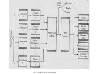
  • 25. Single Channel DAS • The components of data acquisition systems include: -Sensors, to convert physical parameters to electrical signals. -Signal conditioning circuitry, to convert sensor signals into a form that can be converted to digital values. -Analog-to-digital converters, to convert conditioned sensor signals to digital values.
  • 27. Elements of Multichannel DAS • Transducers • Signal Conditioning Equipment • Multiplexer • Calibrating Equipment • Display Equipment
  • 29. Multiplexer • It is the process of sharing a single channel with more than one output • It accepts multiple analog inputs and connects them sequentially to any one output line • ie. Using common transmission channel for transmitting more then one quantity • By Multiplexing cost of transmission and maintenance is reduced
  • 30. Computer based DAS • Computer is equipped with additional hardware for data acquisition and analysis. Also suitable software for data acquisition is loaded. • The software includes programs for accessing the data, perform computations and to display the result. • The data acquisition hardware is a multifunction card, it accepts input analog voltage. This analog voltage is amplified to a standard level and then digitized by a high speed ADC.
  • 31. Configuration of DAS Various significant factors are to be considered while selecting a data acquisition system- • Accuracy and resolution • No. of channels (single/multiple) • Sampling rate per channel • Signal conditioning for each channel • Analog or digital signals • cost
  • 32. Objectives of DAS • To acquire necessary data at correct speed and correct time. • To use all the received data efficiently. • To monitor complete plant operation. • To collect, summarize and store data for diagnosis and record.
  • 33. Applications of DAS • It is used for collecting information • It is used to convert the data into a useful form • It is used to generate information for display • DAS is used in aircraft control system, Electrical power generation, Industrial process system
  • 34. Interfacing of sensors / actuators to DAS
  • 35. Temperature control using DAS • The block diagram shows the processes that are to be carried out in order to control the temperature. • The temperature sensor first senses the temperature around it and gives out a corresponding voltage, which is amplified by the amplifier. • Amplified voltage then goes to the input to DAS • Amplified voltage is read by DAS software and analysis is made and other manipulation are added so as to provide control logic. • Output terminal of the DAS are given to 3 relays which operates Fan, pump motor and heater.
  • 36. Bit width • When analog signal is converted to digital, it is represented in digital form by a series of binary number, each of which represent the signal value. • Thus, the number of binary digits or bits in each word is known as the bit width. • As the more bits the more precisely the binary numbers can represent the signal.
  • 37. Aliasing • In signal processing, aliasing is an effect that causes different signal to become indistinguishable when sampled. • The original signal is reproduced at a wrong frequency this phenomenon is called aliasing. • It occurs when a system is measured at an insufficient sampling rate.
  • 38. Sampling the data • DAS inputs the data from each transducer one at a time. It takes few milliseconds to input the data from one transducer connected to one channel. • Thus for a number of channels it will take certain time. This is called scanning. • The number of times inputting of the data or scanning is done is called as sampling rate or sampling frequency.
  • 39. Sampling rate • The number of times inputting of the data or scanning is done is called as sampling rate. • If the values of these data coming from various transducers is changing with respect to time, then to get variation with time correctly the sampling rate has to be high. ie. Sampling has to be done very fast. • Eg. If data is changing at a frequency n Hz, then sampling frequency has to be equal to or greater than n.
  • 40. Nyquist Sampling Theorem • As per this theorem, if the complete variation of a signal of frequency n with respect to time is to be correctly obtained by sampling then the sampling rate has to be at least 2n. This is called as Nyquist rate. • It is the rate at which an analog signal should be sampled so that it can be faithfully reproduced. As per Nyquist theorem, the sampling rate should be twice as fast as highest frequency of signal being measured or sampled.
  • 41. Sample and Hold Circuit It consists of two steps- Sample- During sampling measured value of physical variable is given to the input module of DAS. This value is converted to a digital output and given to CPU for processing. Hold- This measured value of data sampled at the instant will be held in memory till the next sampling.
  • 42. Role of S/H Circuit • Sample and hold circuit are used to sample or monitor the value of a voltage at frequent conditions. • The sampled value is held till such time it is again sampled. • The sampled voltage is stored in a capacitor by charging it. Hence name sample and hold.
  • 43. Analog to Digital Converter (ADC) • A/D converter is a device that converts a continuous physical quantity (analog signal) to a digital number that represents the quantity's amplitude. • To convert an analog signal to digital the time axis has to be divided into a number of equally spaced interval. This process is known as Quantization. • Types- a) Flash type ADC b) Counter / ramp type ADC c) Successive approximation ADC
  • 45. Successive Approximation ADC • Voltage comparator compares analog input voltage with output of DAC. The comparator is followed by successive approximation register (SAR). • SAR is used to find the required value of each bit by trial and error. • Analog input signal is applied & start command is given now SAR sets the MSB D1=1 with all other bits to 0. • If VA > Vx, The MSB is left at ‘1’ and next LSB is made ‘1’ and further tested. • If VA < Vx, The MSB is resetted to ‘0’ and go on to the next LSB and further tested.
  • 46. Digital to Analog Converter (DAC) • D/A converter takes a digital code (binary signal) as its input and produces an analog voltage or current as its output. This analog output is proportional to the digital input. • The output voltage of DAC is given as Vo = Kv Vref ( b1 2-1 + b2 2-2 +........+ bn 2-n ) • Types- a) Weighted resistor type DAC b) R-2R ladder type DAC
  • 48. R-2R Ladder type ADC • It utilizes resistors of two values ie. R and 2R • The arrangement of resistors are such that the resistance looking into any of the nodes is a uniform value R, with a terminating resistance 2R. • The binary inputs are applied through switches. • Input current to op-amp by binary input is directly proportional to their digit weights. I1 = Vr / 2R, I2 = Vr/2/2R = Vr/4R …..and so on So the corresponding analog signals are produced as output.
  • 49. Motion Control Peripherals:PWM,QEI PWM Module: • Pulse width modulation (PWM) is a simple but powerful technique of using a rectangular digital waveform to control an analog variable or simply controlling analog circuits with a microprocessor's digital outputs. • PWM is employed in a wide variety of applications, from measurement & communications to power control and conversion. • TM4C123GH6PM microcontroller provides motion control functions integrated into the device
  • 50. PWM using TIVA TM4C123GH6PM • TM4C123GH6PM microcontroller contains two PWM modules, each with four PWM generator blocks and a control block, for a total of 16 PWM outputs. • The control block determines the polarity of the PWM signals, and which signals are passed through to the pins. • Three generator blocks can also generate the full six channels of gate controls required by a 3-phase inverter bridge. Each PWM generator block has the following features: • One fault-condition handling inputs to quickly provide low- latency shutdown and prevent damage to the motor being controlled, for a total of two inputs
  • 51. Contd.. • One 16-bit counter  Runs in Down or Up/Down mode  Output frequency controlled by a 16-bit load value  Load value updates can be synchronized  Produces output signals at zero and load value • Two PWM comparators  Comparator value updates can be synchronized  Produces output signals on match • PWM signal generator  Output PWM signal is constructed based on actions taken as a result of the counter and PWM comparator output signals  Produces two independent PWM signals • Dead-band generator  Produces two PWM signals with programmable dead-band delays suitable for driving a half-H bridge.  Can be bypassed, leaving input PWM signals unmodified.
  • 52. Contd.. • The control block determines the polarity of the PWM signals and which signals are passed through to the pins. • The output of the PWM generation blocks are managed by the output control block before being passed to the device pins. • PWM output enable of each PWM signal • Optional output inversion of each PWM signal (polarity control) • Optional fault handling for each PWM signal • Synchronization of timers in the PWM generator blocks • Synchronization of timer/comparator updates across the PWM generator blocks • Extended PWM synchronization of timer/comparator updates across the PWM generator blocks • Interrupt status summary of the PWM generator blocks • Extended PWM fault handling, with multiple fault signals, programmable polarities, and filtering • PWM generators can be operated independently or synchronized with other generators
  • 53. Block Diagram PWM control block: TM4C123GH6PM controller contains two PWM modules, each with four generator blocks that generate eight independent PWM signals or four paired PWM signals with dead- band delays inserted
  • 54. Contd.. PWM Generator block: Functional Description: Clock Configuration The PWM has two clock source options: ■ The System Clock ■ A pre divided System Clock The clock source is selected by programming the USPWMDIV bit in the Run-Mode Clock Configuration (RCC) register at System Control offset 0x060. The PWMDIV bit field specifies the divisor of the System Clock that is used to create the PWM Clock.
  • 55. PWM Timer • The timer in each PWM generator runs in one of two modes: Count- Down mode or Count-Up/Down mode. • In Count-Down mode, the timer counts from the load value to zero, goes back to the load value, and continues counting down. • In Count-Up/Down mode, the timer counts from zero up to the load value, back down to zero, back up to the load value, and so on. • Generally, Count-Down mode is used for generating left- or right-aligned PWM signals, while the Count-Up/Down mode is used for generating center-aligned PWM signals. • The timers output three signals that are used in the PWM generation process: the direction signal (this is always Low in Count-Down mode, but alternates between low and high in Count-Up/Down mode), a single- clock-cycle-width High pulse when the counter is zero, and a single-clock- cycle-width High pulse when the counter is equal to the load value. • Note that in Count-Down mode, the zero pulse is immediately followed by the load pulse. In the figures in this chapter, these signals are labelled "dir," "zero," and "load."
  • 56. Contd.. PWM Comparators: • Each PWM generator has two comparators that monitor the value of the counter, when either comparator matches the counter, they output a single-clock-cycle- width High pulse, labeled "cmpA" and "cmpB. • When in Count-Up/Down mode, these comparators match both when counting up and when counting down, and thus are qualified by the counter direction signal. • These qualified pulses are used in the PWM generation process. If either comparator match value is greater than the counter load value, then that comparator never outputs a High pulse.
  • 57. Contd.. PWM Count-Down Mode PWM Count- Up/Down Mode
  • 58. PWM Signal Generator: • Each PWM generator takes the load, zero, cmpA, and cmpB pulses (qualified by the dir signal) and generates two internal PWM signals, pwmA and pwmB. • In Count-Down mode, there are four events that can affect these signals: zero, load, match A down, and match B down. • In Count-Up/Down mode, there are six events that can affect these signals: zero, load, match A down, match A up, match B down, and match B up. • The match A or match B events are ignored when they coincide with the zero or load events. If the match A and match B events coincide, the first signal, pwmA, is generated based only on the match A event, and the second signal, pwmB, is generated based only on the match B event.
  • 59. Dead-Band Generator: • The pwmA and pwmB signals produced by each PWM generator are passed to the dead-band generator. If the dead-band generator is disabled, the PWM signals simply pass through to the pwmA' and pwmB' signals unmodified. • If the dead-band generator is enabled, the pwmB signal is lost and two PWM signals are generated based on the pwmA signal. • The first output PWM signal, pwmA' is the pwmA signal with the rising edge delayed by a programmable amount. The second output PWM signal, pwmB', is the inversion of the pwmA signal with a programmable delay added between the falling edge of the pwmA signal and the rising edge of the pwmB' signal. • The resulting signals are a pair of active high signals where one is always high, except for a programmable amount of time at transitions where both are low. • These signals are therefore suitable for driving a half-H bridge, with the dead- band delays preventing shoot-through current from damaging the power electronics.
  • 60. Quadrature Encoder Interface (QEI) • The Quadrature Encoder Interface (QEI) module provides the interface to incremental encoders for obtaining mechanical position data. Quadrature encoders, also known as 2-channel incremental encoders or optical encoders, detect position and speed of rotating motion systems. • A quadrature encoder converts linear displacement into a pulse signal. • By monitoring both the number of pulses and the relative phase of the two signals, you can track the position, direction of rotation, and speed. In addition, a third channel, or index signal, can be used to reset the position counter. • A classic quadrature encoder has a slotted wheel like structure, to which a shaft of the motor is attached and a detector module that captures the movement of slots in the wheel.
  • 61. Interfacing QEI using TIVA TM4C123GH6PM • The TM4C123GH6PM microcontroller includes two quadrature encoder interface (QEI) modules. • Each QEI module interprets the code produced by a quadrature encoder wheel to integrate position over time and determine direction of rotation. In addition, it can capture a running estimate of the velocity of the encoder wheel. Figure: QEI Input Signal Logic
  • 62. • The TM4C123GH6PM microcontroller includes two QEI modules providing control of two motors at the same time with the following features: -Position integrator that tracks the encoder position -Programmable noise filter on the inputs -Velocity capture using built-in timer -The input frequency of the QEI inputs may be as high as 1/4 of the processor frequency (for example, 12.5 MHz for a 50-MHz system) Interrupt generation on: • Index pulse • Velocity-timer expiration • Direction change • Quadrature error detection
  • 63. Functional Description • The QEI module interprets the two-bit gray code produced by a quadrature encoder wheel to integrate position over time and determine direction of rotation. • In addition, it can capture a running estimate of the velocity of the encoder wheel. • The position integrator and velocity capture can be independently enabled, though the position integrator must be enabled before the velocity capture can be enabled. • The two phase signals, PhAn and PhBn, can be swapped before being interpreted by the QEI module to change the meaning of forward and backward and to correct for misfiring of the system. • Alternatively, the phase signals can be interpreted as a clock and direction signal as output by some encoders.
  • 65. Contd.. • The QEI module input signals have a digital noise filter on them that can be enabled to prevent spurious operation. • The noise filter requires that the inputs be stable for a specified number of consecutive clock cycles before updating the edge detector. • The filter is enabled by the FILTEN bit in the QEI Control (QEICTL) register. The frequency of the input update is programmable using the • FILTCNT bit field in the QEICTL register. • The QEI module supports two modes of signal operation: • Quadrature phase mode, the encoder produces two clocks that are 90 degrees out of phase, the edge relationship is used to determine the direction of rotation. • Clock/direction mode, the encoder produces a clock signal to indicate steps and a direction signal to indicate the direction of rotation. This mode is determined by the SIGMODE bit of the QEICTL register.
  • 66. • When the QEI module is set to use the quadrature phase mode (SIGMODE bit is clear), the capture mode for the position integrator can be set to update the position counter on every edge of the PhA signal or to update on every edge of both PhA and PhB. • Updating the position counter on every PhA and PhB edge provides more positional resolution at the cost of less range in the positional counter. • When edges on PhA lead edges on PhB, the position counter is incremented. When edges on PhB lead edges on PhA, the position counter is decremented. • When a rising and falling edge pair is seen on one of the phases without any edges on the other, the direction of rotation has changed.
  • 67. The positional counter is automatically reset on one of two conditions: - Sensing the index pulse or -Reaching the maximum position value. • The reset mode is determined by the RESMODE bit of the QEICTL register. • When RESMODE is set, the positional counter is reset when the index pulse is sensed. • This mode limits the positional counter to the values [0: N-1], where N is the number of phase edges in a full revolution of the encoder wheel. • The QEI Maximum Position (QEIMAXPOS) register must be programmed with N-1 so that the reverse direction from position 0 can move the position counter to N-1. • In this mode, the position register contains the absolute position of the encoder relative to the index (or home) position once an index pulse has been seen.
  • 68. – When RESMODE is clear, the positional counter is constrained to the range [0: M], where M is the programmable maximum value. – The index pulse is ignored by the positional counter in this mode. Velocity capture uses a configurable timer and a count register. The timer counts the number of phase edges (using the same configuration as for the position integrator) in a given time period. • The edge count from the previous time period is available to the controller via the QEI Velocity (QEISPEED) register, while the edge count for the current time period is being accumulated in the QEI Velocity Counter (QEICOUNT) register. • As soon as the current time period is complete, the total number of edges counted in that time period is made available in the QEISPEED register (overwriting the previous value), the QEICOUNT register is cleared, and counting commences on a new time period. • The number of edges counted in a given time period is directly proportional to the velocity of the encoder.