Vlsi design process for low power design methodology using reconfigurable fpga
1 like148 views

The document discusses a reconfigurable FPGA (eFPGA) architecture designed for low-power applications in the context of VLSI design. It highlights the advantages of using eFPGAs, such as flexibility and efficiency in energy and area, while presenting a self-contained design methodology for creating domainspecific eFPGAs. The proposed system allows for automation in configuration, layout generation, and verification, thereby streamlining the design process.
![IJRET: International Journal of Research in Engineering and Technology ISSN: 2319-1163
__________________________________________________________________________________________
Volume: 01 Issue: 03 | Nov-2012, Available @ http://www.ijret.org 516
VLSI DESIGN PROCESS FOR LOW POWER DESIGN METHODOLOGY
USING RECONFIGURABLE FPGA
R. Rajendra Prasad1
, M. V. Subramanyam2
, K. Satya Prasad3
1
Asso.professor of ECE Department, N.B.K.R.Institute of Science and Technology, Vidyanagar, S. P. S. R. Nellore ,
Andhra Pradesh, India. rajendra_831@yahoo.co.in, rechalabhi812@gmail.com
2
Principal and Prof ECE Department, Santhi Ram Engineering College, Nandyal, India, mvsraj@yahoo.com
3
Professor of ECE Department and Rector, JNTU Kakinada, Kakinada, India., prasad_kodati@yahoo.co.in
Abstract
Modern digital processing applications have an increasing demand for computational power while needing to preserve low power
dissipation and high flexibility. For many applications, the growth of algorithmic complexity is already faster than the growth of
computational power provided by discrete general-purpose processors. A typical approach to address this problem is the combination
of a processor core with dedicated accelerators. Since changes in standards or algorithms can change the demands on the
accelerators, an attractive alternative to highly customized VLSI macros is suggested with the usage of reconfigurable embedded
FPGAs (eFPGAs).
Keyword: embedded FPGA, Fast computing, Hybrid design.
------------------------------------------------------------------------***----------------------------------------------------------------------
1. INTRODUCTION
FPGAs are widely used as an attractive compromise between
highly efficient physically optimized VLSI designs and
software programmable processors. Due to their
reconfigurability, FPGAs are highly flexible and allow for
relatively short design cycles since no physical changes to the
underlying hardware have to be made in case of a redesign.
However, they offer lower physical implementation costs
compared to software programmable processors, as the
inherent parallelism of many algorithms can be exploited in
contrast to sequential processor architectures. As a result,
commercial FPGA-architectures have been optimized to suit a
wide variety of applications from network related and digital
signal processing to the realization of soft-core processors. For
an embedded FPGA used as configurable accelerator,
however, the requirements concerning the provided resources
are often well defined and much narrower than for discrete or
“general purpose” FPGAs. Hence, eFPGAs can be optimized
for a certain set of applications and thus achieve higher
efficiency in terms of power dissipation, area and speed. First
investigations on a reconfigurable ASIP with a reconfigurable
accelerator based on a parametrisable eFPGA-architecture
have shown significant improvements in energy- and area-
efficiency [5].
2. eFPGA-ARCHITECTURE
The eFPGA architecture presented here is based on a highly
parametrisable architecture template targeting an arithmetic-
oriented application domain. Some of them are described by a
single value (e.g. the number of LEs in a row and Column),
while others require a more complex definition (e.g. the
connectivity per switch point). In the following, the
architectural components and the according parameters are
discussed in detail. A typical characteristic of arithmetic data
paths is the organization in function slices and bit slices. A
function slice represents one of many consecutively processed
elementary functions (e.g. n-bit addition, n-bit XOR operation
etc.), while a bit slice represents all processing elements in the
same column corresponding to the same bit value (e.g. bit 0 of
two successive function slices).
Typical arithmetic data path scheme most communication
between function slices and bit slices is local, i.e. only
between direct neighbors. In addition, operands are typically
fed to the data path using a broadcast scheme. The eFPGA-
architecture reflects typical arithmetic data path schemes by
using two-dimensional clusters of logic elements with a
distributed interconnect rather than one-dimensional clusters
with a central connection box. The signals coming from the
connection box are distributed to the logic elements in rows
and columns according to the function slices and bit slices,
such that all logic elements in a row or column share the same
input signals using so-called broadcast lines. This reduces the
number of signals that need to be provided by the connection
box and hence reduces the significant overhead imposed by
the configurable connection boxes.
The size of the cluster can be varied in the horizontal and
vertical direction independently. Also, the number of
broadcast lines per row and column can be changed in designs
based on the template. Broadcast lines can be fed to the cluster](https://image.slidesharecdn.com/vlsidesignprocessforlowpowerdesignmethodologyusingreconfigurablefpga-160728133256/85/Vlsi-design-process-for-low-power-design-methodology-using-reconfigurable-fpga-1-320.jpg)
![IJRET: International Journal of Research in Engineering and Technology ISSN: 2319-1163
__________________________________________________________________________________________
Volume: 01 Issue: 03 | Nov-2012, Available @ http://www.ijret.org 517
from all four directions, and in the same way the outputs of the
LEs at all four cluster borders can be fed to the connection
box. The actual connectivity can be any set of the four
possible data directions (north, east, south, west) for inputs
and outputs independently. Between adjacent clusters, feed
through stages are provided to use the broadcast lines of the
neighboring clusters as inputs for the current cluster, hence
creating virtually larger clusters by cascading several of them.
a) Logic elements
The local connectivity between the logic elements is provided
by dedicated routing blocks (DRB) located in the logic
element. Each DRB is a set of multiplexes used to connect
broadcast signals or local signals to the core logic of the logic
element. The actual connectivity can be defined in the
architecture template by stating all sources connected to the
DRBs with their offset to the actual LE. The functionality of
the core logic itself is specified by a list of elementary
Boolean functions that the LE can process (e.g. full addition,
gated full addition etc.). Registers can be inserted per logic
element or with a reduced density, e.g. every second LE-row.
Cluster broadcast line core logic dedicated routing block
(DRB) broadcast lines local Connections.
b) Configuration memories
To reduce the overhead of the memory cells (typically
SRAMs) used to store the configuration of the FPGAs logic
and routing resources, the present architecture template allows
for sharing the configuration bits and thus configuring several
adjacent elements identically. This scheme is applied to the
logic elements as well as to the interconnect resources, where
adjacent switch points or connection points can share a single
SRAM block. The degree of SRAM sharing can be adjusted in
the architecture template in reasonable limits.
c) Routing switch
The routing switch of an FPGA is a set of switch points those
are located at crossing points of horizontal and vertical routing
tracks. The number of switch points available as well as their
connectivity determines the flexibility of the complete routing
switch. It was shown that it is not necessary to provide a fully
populated routing switch to achieve a good amount of
flexibility [6]. The architecture template presented here is very
flexible concerning the definition of available routing
resources. The number of routing tracks in horizontal and
vertical direction can be chosen independently. Each switch
point is defined by its position in the matrix of crossing lines
as well as the connectivity inside the switch point. Different
switch points can have different flexibility. In addition, the
segmentation of the interconnect can be adjusted by assigning
each routing track a certain segment length, corresponding to
the number of routing switches that are bypassed before the
line connects to the next routing switch.
d) Connection box
Finally, the architecture template offers a highly flexible
description of the connection box similar to the routing switch
definition. Three types of routing channels are supported: fully
connected, periodic connectivity and unconnected. Fully
connected tracks offer full population of the connection box,
i.e. each track can connect to each according broadcast line of
a cluster. However, they have the highest implementation
costs. Unconnected tracks can be implemented for fast signal
routing, as the capacitive load of these wires can be kept very
low. Periodic tracks use a special connection type best suited
for arithmetic data paths, where signals on a bus are typically
ordered by the weight of their bits. Accordingly, periodic
routing channels have a window of connection points that
slides across the tracks with a given velocity. The connection
box defined in the architecture template can be composed of
any mix of tracks with different channel widths and sliding
window specifications.
3. PROPOSED SYSTEM DESIGN
As many of the architectural features in the presented eFPGA
are unique and not common in standard FPGAs, there is
currently no tool support available. Most research conducted
in the field of eFPGA-architectures is based on the VPR
design flow [7] which can only be used to model standard
island style FPGA-architectures with LUT-based logic
elements and a small choice of routing switch architectures.
Hence, an important goal of this work is the creation of a self-
contained design methodology to design application domain
specific eFPGAs and the according basic tool support.
Figure 1: design flow for the implementation of layout design
The architecture template described above was formulated as a
high level description using C language. Based on this
architecture description, three main steps are supported by the
design flow. First, a layout generator creates a VLSI-layout of
the specified eFPGA based on a small set of handcrafted,](https://image.slidesharecdn.com/vlsidesignprocessforlowpowerdesignmethodologyusingreconfigurablefpga-160728133256/85/Vlsi-design-process-for-low-power-design-methodology-using-reconfigurable-fpga-2-320.jpg)
![IJRET: International Journal of Research in Engineering and Technology ISSN: 2319-1163
__________________________________________________________________________________________
Volume: 01 Issue: 03 | Nov-2012, Available @ http://www.ijret.org 518
physically optimized basic cells such as the multiplexes for the
DRB or the switch points of the routing switch. Several
studies concerning this part of the design flow have been
published before [8] [9]. While the first automatically
generated eFPGA-layouts still needed to be configured
manually (i.e. each SRAM cell had to be configured with the
proper value), an automatic bit stream generator supporting
the complete architecture template is currently under
construction. The configuration bit stream is used to conduct
net list simulations based on layout-extracted net lists. To
verify the functionality of the eFPGA-macro, a VHDL-
generator creates a functional description that can be
simulated using common simulation tools like ModelSim. The
output of the configuration is based on a net list that describes
the signal flow graph mapped to the eFPGA. Currently, the net
list description is still complex, as each logic element and each
routing resource has to be described here. However, for
arithmetic data paths this net list is highly regular which
reduces the effort to generate it manually. Currently, a very
time-consuming and error-prone work is the generation of the
configuration bits and the routing of signals between the logic
elements. The placement process is less complex due to the
regularity of the examples considered here i.e. arithmetic data
paths. Consequently, a future step will be the implementation
of a routing tool supporting the parametrisable architecture.
Similar approaches to automatic eFPGA design have been
proposed e.g. with GILES [10] or PYTHAGOR [11].
However, those design flows have significant constraints
regarding the FPGA-architectures (e.g. only island style
FPGAs are supported) and the physical implementation style.
As an example, using standard cell implementations (e.g.
proposed by PYTHAGOR) leads to unfavorable physical
implementation costs concerning area, performance and power
dissipation. The first results presented here are based on a
completely functional co design of a routing switch layout, the
according VHDL model and the configuration bit stream
based on a given net list.
a) Layout generator
The layout generator is based on a prior work on Automated
VLSI-design of regular data paths [12]. This so-called data
path generator uses a textual description of a signal flow graph
(SFG) and a small set of hand designed layout cells to
generate a layout. Since the textual SFG description can be
parameterized, the data path generator allows for a very
flexible implementation process, e.g. when parameters like
word lengths are changed in the SFG. Starting from the C-
based high level description of the eFPGA architecture a data
path generator suited SFG description is automatically
generated. Due to the highly modular design style, the
eFPGA-macro can be ported to different CMOS-technologies
with small effort, since only few hand designed layout cells
are required. After the layout is generated, standard net list
extraction and simulation tools can be used to characterize the
eFPGA macro in terms of area, timing and power dissipation.
b) VHDL-generator
Based on the architecture description, a VHDL-model of the
eFPGA is created automatically. It incorporates the functional
description of the basic configurable elements like routing
switch points or logic elements and combines them according
to the architectural parameters. The VHDL-model of the
eFPGA is used to verify the functionality defined by the net
list using existing simulation tools. It is also useful to test the
eFPGA macro created by the layout generator for correctness
by co simulation of the layout extracted net list and the
functional VHDL model.
c) Configuration
To enable simulations of the eFPGA-macro (on functional as
well as on net list level), all configuration bits have to be set
properly. Due to the very large number of configuration bits, it
is necessary to have an automated way of creating the bit
stream from the mapped net list. Existing bit stream generators
like DAGGER [13] lack the Support for highly
parametrisable eFPGA architectures as the one described here.
The configuration elaborated as part of the design
methodology presented here creates configuration bit streams
based on the net list and the architecture specifications. It also
uses the information from the layout generator to determine
the actual position of all blocks to be configured in the macro.
The configuration bit stream is composed of elementary
configuration table entries that must be provided for the basic
eFPGA elements like routing switch points or logic elements.
The elementary tables can be created with small effort, as only
few bits are required to configure these basic elements. The bit
stream is then concatenated according to the position of the
elements in the overall macro.
4. DESIGN EXAMPLE
As a first step in verifying the proposed design Methodology,
routing switches generator comprising all elements of the
design flow was implemented. As an example, a routing
switch with 32 tracks both in horizontal and vertical direction
was specified in the according architecture description. Switch
points with different flexibility are provided as exemplary
basic components for the routing switch. As the C based
description is on an abstract level, the architecture
specification for the complete routing switch can be created
within few minutesThree global parameters describe the
channel widths and the use of configuration sharing . Each
switch point is defined by a set of potential signal routes
according to their input and output directions (north, east,
south, west). From the flexibility required by each switch
point, the routing switch generator extracts a set of basic
layout cells that need to be designed for the VLSI-
implementation. The design of the according switch point
macros and the SRAM-cell required for the configuration
storage takes some hours for a skilled designer.The layout
generator automatically determines the optimum placement of
the basic cells for a given aspect ratio of the routing switch. It
also calculates the optimum aspect ratios of the configuration](https://image.slidesharecdn.com/vlsidesignprocessforlowpowerdesignmethodologyusingreconfigurablefpga-160728133256/85/Vlsi-design-process-for-low-power-design-methodology-using-reconfigurable-fpga-3-320.jpg)
![IJRET: International Journal of Research in Engineering and Technology ISSN: 2319-1163
__________________________________________________________________________________________
Volume: 01 Issue: 03 | Nov-2012, Available @ http://www.ijret.org 520
REFERENCES
[1] J. Hauser, “Integrated Circuits for Next Generation
Wireless Systems”, Proceedings of the European Solid- State
Circuits Conference (ESSCIRC) 2001, pp. 26-29
[2] Stretch S6000, http://www.stretchinc.com
[3] MENTA eFPGA-augmented RISC CPUs (website),
http://www.menta.fr/efpga_cpu.html
[4] A. Ye and J. Rose, “Using Bus-Based Connections to
Improve Field-Programmable Gate Array Density
Implementing Data path Circuits”,IEEE Transactions on Very
Large Scale Integration (VLSI) Systems, Vol. 14, No. 5, pp.
462-473, May 2006.
[5] T. von Sydow, M. Korb, B. Neumann, H. Blume and T. G.
Noll, “Modeling and Quantitative Analysis of Coupling
Mechanisms of Programmable Processor Cores and
Arithmetic Oriented eFPGA-macros”, in Proc. Reconfigurable
Computing and FPGA's, pp. 252-261, 2006.
[6] G. Lemieux and D. Lewis, “Design of Interconnection
Networks for Programmable Logic” Kluwer Academic
Publishers, 2004.
[7] V. Betz, J. Rose and A. Marquardt, “Architecture and
CAD for Deep-Sub micron FPGAs” in Kluwer International
Series in Engineering and Computer Science, 1999.
[8] T. von Sydow, B. Neumann, H. Blume and T. G. Noll,
“Quantitative Analysis of embedded FPGA Architectures for
Arithmetic”, in Proc. Application Specific Systems,
Architectures and Processors Conference ,pp. 125-131, 2006.
[9] B. Neumann, T. von Sydow, H. Blume and T. G. Noll,
“Design and quantitative analysis of parametrisable eFPGA-
architectures for arithmetic“ in Advances in Radio Science,
Vol. 4, pp. 251-259, 2006.
[10] I. Kuon, A. Egier and J. Rose, “Design, Layout and
Verification of an FPGA using Automated Tools”, in Proc.
2005 ACM/SIGDA 13th international symposium on Field
programmable gate arrays, pp. 215–226, 2005.
[11] A. Danilin, M. Bennebroek and S. Sawitzki, “A novel
toolset for the development of FPGA-like reconfigurable
logic”, in Proc. FPL 2005, pp. 640-643, 2005.
[12] O. Weiss, M. Gansen and T. G. Noll, “A flexible
Datapath Generator for Physical Oriented Design” in Proc.
European Solid-State Circuits Conference, pp. 408-411, 2001.
[13] K. Siozios et. al, “DAGGER: A Novel Generic
Methodology for FPGA Bitstream Generation and its Software
Tool Implementation”, in Proc. Parallel and Distributed
Processing Symposium 2005,p.p. 165b, 2005.](https://image.slidesharecdn.com/vlsidesignprocessforlowpowerdesignmethodologyusingreconfigurablefpga-160728133256/85/Vlsi-design-process-for-low-power-design-methodology-using-reconfigurable-fpga-5-320.jpg)
Vlsi design process for low power design methodology using reconfigurable fpga
- 1. IJRET: International Journal of Research in Engineering and Technology ISSN: 2319-1163 __________________________________________________________________________________________ Volume: 01 Issue: 03 | Nov-2012, Available @ http://www.ijret.org 516 VLSI DESIGN PROCESS FOR LOW POWER DESIGN METHODOLOGY USING RECONFIGURABLE FPGA R. Rajendra Prasad1 , M. V. Subramanyam2 , K. Satya Prasad3 1 Asso.professor of ECE Department, N.B.K.R.Institute of Science and Technology, Vidyanagar, S. P. S. R. Nellore , Andhra Pradesh, India. rajendra_831@yahoo.co.in, rechalabhi812@gmail.com 2 Principal and Prof ECE Department, Santhi Ram Engineering College, Nandyal, India, mvsraj@yahoo.com 3 Professor of ECE Department and Rector, JNTU Kakinada, Kakinada, India., prasad_kodati@yahoo.co.in Abstract Modern digital processing applications have an increasing demand for computational power while needing to preserve low power dissipation and high flexibility. For many applications, the growth of algorithmic complexity is already faster than the growth of computational power provided by discrete general-purpose processors. A typical approach to address this problem is the combination of a processor core with dedicated accelerators. Since changes in standards or algorithms can change the demands on the accelerators, an attractive alternative to highly customized VLSI macros is suggested with the usage of reconfigurable embedded FPGAs (eFPGAs). Keyword: embedded FPGA, Fast computing, Hybrid design. ------------------------------------------------------------------------***---------------------------------------------------------------------- 1. INTRODUCTION FPGAs are widely used as an attractive compromise between highly efficient physically optimized VLSI designs and software programmable processors. Due to their reconfigurability, FPGAs are highly flexible and allow for relatively short design cycles since no physical changes to the underlying hardware have to be made in case of a redesign. However, they offer lower physical implementation costs compared to software programmable processors, as the inherent parallelism of many algorithms can be exploited in contrast to sequential processor architectures. As a result, commercial FPGA-architectures have been optimized to suit a wide variety of applications from network related and digital signal processing to the realization of soft-core processors. For an embedded FPGA used as configurable accelerator, however, the requirements concerning the provided resources are often well defined and much narrower than for discrete or “general purpose” FPGAs. Hence, eFPGAs can be optimized for a certain set of applications and thus achieve higher efficiency in terms of power dissipation, area and speed. First investigations on a reconfigurable ASIP with a reconfigurable accelerator based on a parametrisable eFPGA-architecture have shown significant improvements in energy- and area- efficiency [5]. 2. eFPGA-ARCHITECTURE The eFPGA architecture presented here is based on a highly parametrisable architecture template targeting an arithmetic- oriented application domain. Some of them are described by a single value (e.g. the number of LEs in a row and Column), while others require a more complex definition (e.g. the connectivity per switch point). In the following, the architectural components and the according parameters are discussed in detail. A typical characteristic of arithmetic data paths is the organization in function slices and bit slices. A function slice represents one of many consecutively processed elementary functions (e.g. n-bit addition, n-bit XOR operation etc.), while a bit slice represents all processing elements in the same column corresponding to the same bit value (e.g. bit 0 of two successive function slices). Typical arithmetic data path scheme most communication between function slices and bit slices is local, i.e. only between direct neighbors. In addition, operands are typically fed to the data path using a broadcast scheme. The eFPGA- architecture reflects typical arithmetic data path schemes by using two-dimensional clusters of logic elements with a distributed interconnect rather than one-dimensional clusters with a central connection box. The signals coming from the connection box are distributed to the logic elements in rows and columns according to the function slices and bit slices, such that all logic elements in a row or column share the same input signals using so-called broadcast lines. This reduces the number of signals that need to be provided by the connection box and hence reduces the significant overhead imposed by the configurable connection boxes. The size of the cluster can be varied in the horizontal and vertical direction independently. Also, the number of broadcast lines per row and column can be changed in designs based on the template. Broadcast lines can be fed to the cluster
- 2. IJRET: International Journal of Research in Engineering and Technology ISSN: 2319-1163 __________________________________________________________________________________________ Volume: 01 Issue: 03 | Nov-2012, Available @ http://www.ijret.org 517 from all four directions, and in the same way the outputs of the LEs at all four cluster borders can be fed to the connection box. The actual connectivity can be any set of the four possible data directions (north, east, south, west) for inputs and outputs independently. Between adjacent clusters, feed through stages are provided to use the broadcast lines of the neighboring clusters as inputs for the current cluster, hence creating virtually larger clusters by cascading several of them. a) Logic elements The local connectivity between the logic elements is provided by dedicated routing blocks (DRB) located in the logic element. Each DRB is a set of multiplexes used to connect broadcast signals or local signals to the core logic of the logic element. The actual connectivity can be defined in the architecture template by stating all sources connected to the DRBs with their offset to the actual LE. The functionality of the core logic itself is specified by a list of elementary Boolean functions that the LE can process (e.g. full addition, gated full addition etc.). Registers can be inserted per logic element or with a reduced density, e.g. every second LE-row. Cluster broadcast line core logic dedicated routing block (DRB) broadcast lines local Connections. b) Configuration memories To reduce the overhead of the memory cells (typically SRAMs) used to store the configuration of the FPGAs logic and routing resources, the present architecture template allows for sharing the configuration bits and thus configuring several adjacent elements identically. This scheme is applied to the logic elements as well as to the interconnect resources, where adjacent switch points or connection points can share a single SRAM block. The degree of SRAM sharing can be adjusted in the architecture template in reasonable limits. c) Routing switch The routing switch of an FPGA is a set of switch points those are located at crossing points of horizontal and vertical routing tracks. The number of switch points available as well as their connectivity determines the flexibility of the complete routing switch. It was shown that it is not necessary to provide a fully populated routing switch to achieve a good amount of flexibility [6]. The architecture template presented here is very flexible concerning the definition of available routing resources. The number of routing tracks in horizontal and vertical direction can be chosen independently. Each switch point is defined by its position in the matrix of crossing lines as well as the connectivity inside the switch point. Different switch points can have different flexibility. In addition, the segmentation of the interconnect can be adjusted by assigning each routing track a certain segment length, corresponding to the number of routing switches that are bypassed before the line connects to the next routing switch. d) Connection box Finally, the architecture template offers a highly flexible description of the connection box similar to the routing switch definition. Three types of routing channels are supported: fully connected, periodic connectivity and unconnected. Fully connected tracks offer full population of the connection box, i.e. each track can connect to each according broadcast line of a cluster. However, they have the highest implementation costs. Unconnected tracks can be implemented for fast signal routing, as the capacitive load of these wires can be kept very low. Periodic tracks use a special connection type best suited for arithmetic data paths, where signals on a bus are typically ordered by the weight of their bits. Accordingly, periodic routing channels have a window of connection points that slides across the tracks with a given velocity. The connection box defined in the architecture template can be composed of any mix of tracks with different channel widths and sliding window specifications. 3. PROPOSED SYSTEM DESIGN As many of the architectural features in the presented eFPGA are unique and not common in standard FPGAs, there is currently no tool support available. Most research conducted in the field of eFPGA-architectures is based on the VPR design flow [7] which can only be used to model standard island style FPGA-architectures with LUT-based logic elements and a small choice of routing switch architectures. Hence, an important goal of this work is the creation of a self- contained design methodology to design application domain specific eFPGAs and the according basic tool support. Figure 1: design flow for the implementation of layout design The architecture template described above was formulated as a high level description using C language. Based on this architecture description, three main steps are supported by the design flow. First, a layout generator creates a VLSI-layout of the specified eFPGA based on a small set of handcrafted,
- 3. IJRET: International Journal of Research in Engineering and Technology ISSN: 2319-1163 __________________________________________________________________________________________ Volume: 01 Issue: 03 | Nov-2012, Available @ http://www.ijret.org 518 physically optimized basic cells such as the multiplexes for the DRB or the switch points of the routing switch. Several studies concerning this part of the design flow have been published before [8] [9]. While the first automatically generated eFPGA-layouts still needed to be configured manually (i.e. each SRAM cell had to be configured with the proper value), an automatic bit stream generator supporting the complete architecture template is currently under construction. The configuration bit stream is used to conduct net list simulations based on layout-extracted net lists. To verify the functionality of the eFPGA-macro, a VHDL- generator creates a functional description that can be simulated using common simulation tools like ModelSim. The output of the configuration is based on a net list that describes the signal flow graph mapped to the eFPGA. Currently, the net list description is still complex, as each logic element and each routing resource has to be described here. However, for arithmetic data paths this net list is highly regular which reduces the effort to generate it manually. Currently, a very time-consuming and error-prone work is the generation of the configuration bits and the routing of signals between the logic elements. The placement process is less complex due to the regularity of the examples considered here i.e. arithmetic data paths. Consequently, a future step will be the implementation of a routing tool supporting the parametrisable architecture. Similar approaches to automatic eFPGA design have been proposed e.g. with GILES [10] or PYTHAGOR [11]. However, those design flows have significant constraints regarding the FPGA-architectures (e.g. only island style FPGAs are supported) and the physical implementation style. As an example, using standard cell implementations (e.g. proposed by PYTHAGOR) leads to unfavorable physical implementation costs concerning area, performance and power dissipation. The first results presented here are based on a completely functional co design of a routing switch layout, the according VHDL model and the configuration bit stream based on a given net list. a) Layout generator The layout generator is based on a prior work on Automated VLSI-design of regular data paths [12]. This so-called data path generator uses a textual description of a signal flow graph (SFG) and a small set of hand designed layout cells to generate a layout. Since the textual SFG description can be parameterized, the data path generator allows for a very flexible implementation process, e.g. when parameters like word lengths are changed in the SFG. Starting from the C- based high level description of the eFPGA architecture a data path generator suited SFG description is automatically generated. Due to the highly modular design style, the eFPGA-macro can be ported to different CMOS-technologies with small effort, since only few hand designed layout cells are required. After the layout is generated, standard net list extraction and simulation tools can be used to characterize the eFPGA macro in terms of area, timing and power dissipation. b) VHDL-generator Based on the architecture description, a VHDL-model of the eFPGA is created automatically. It incorporates the functional description of the basic configurable elements like routing switch points or logic elements and combines them according to the architectural parameters. The VHDL-model of the eFPGA is used to verify the functionality defined by the net list using existing simulation tools. It is also useful to test the eFPGA macro created by the layout generator for correctness by co simulation of the layout extracted net list and the functional VHDL model. c) Configuration To enable simulations of the eFPGA-macro (on functional as well as on net list level), all configuration bits have to be set properly. Due to the very large number of configuration bits, it is necessary to have an automated way of creating the bit stream from the mapped net list. Existing bit stream generators like DAGGER [13] lack the Support for highly parametrisable eFPGA architectures as the one described here. The configuration elaborated as part of the design methodology presented here creates configuration bit streams based on the net list and the architecture specifications. It also uses the information from the layout generator to determine the actual position of all blocks to be configured in the macro. The configuration bit stream is composed of elementary configuration table entries that must be provided for the basic eFPGA elements like routing switch points or logic elements. The elementary tables can be created with small effort, as only few bits are required to configure these basic elements. The bit stream is then concatenated according to the position of the elements in the overall macro. 4. DESIGN EXAMPLE As a first step in verifying the proposed design Methodology, routing switches generator comprising all elements of the design flow was implemented. As an example, a routing switch with 32 tracks both in horizontal and vertical direction was specified in the according architecture description. Switch points with different flexibility are provided as exemplary basic components for the routing switch. As the C based description is on an abstract level, the architecture specification for the complete routing switch can be created within few minutesThree global parameters describe the channel widths and the use of configuration sharing . Each switch point is defined by a set of potential signal routes according to their input and output directions (north, east, south, west). From the flexibility required by each switch point, the routing switch generator extracts a set of basic layout cells that need to be designed for the VLSI- implementation. The design of the according switch point macros and the SRAM-cell required for the configuration storage takes some hours for a skilled designer.The layout generator automatically determines the optimum placement of the basic cells for a given aspect ratio of the routing switch. It also calculates the optimum aspect ratios of the configuration
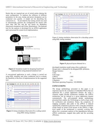
- 4. IJRET: International Journal of Research in Engineering and Technology ISSN: 2319-1163 __________________________________________________________________________________________ Volume: 01 Issue: 03 | Nov-2012, Available @ http://www.ijret.org 519 blocks that are required per set of switch points sharing the same configuration. To analyses the influence of different parameters on the area, timing and power dissipation can be conducted very quickly. A simple net list describing the connections to be provided by the routing switch was used to automatically generate the configuration bit stream with more than 200 bits and the test bench for ModelSim (functional simulation) and Xilinx (Realization). The backend tool for the analysis is developed for an eFPGA application and is processed for system level implementation. Figure 2: Simulation model for designing board level implementation using proposed analytical tool A conventional application to such a design is carried out using HDL simulator and xilinx synthesizer tool to evaluate the feasibility of the flow of implementations for the suggested tool. Figure 3: timing simulation observation for a coding system using HDL timing simulator Figure 4: timing simulation observation for a decoding system using HDL timing simulator Figure 5: physical layout obtained for a developed simulation model using xilinx synthesizer Design static’s obtained fro the designed HDL definition. Design Statistics # IOs : 6 Cell Usage : # BELS : 1041 Macro Statistics # Registers : 156 Maximum operating Frequency: 102.008MHz CONCLUSIONS The design methodology presented in this paper is an important step for the evaluation of embedded FPGAs that are optimized for a certain application domain. By using a common, highly flexible architecture template, the eFPGA architecture can be tailored to a given application domain systematically. The self-contained design methodology presented here enables the VLSI-design as well as basic tools for verification and simulation. Hence, the complexity of mapping exemplary data paths to the eFPGA is reduced significantly compared to previous work. Using the simulation results based on actual VLSI layouts of the eFPGA, a high- level model of the architecture is currently evolving that allows for a systematic analysis of the dependencies between eFPGA architecture, mapped data paths and the according efficiency.
- 5. IJRET: International Journal of Research in Engineering and Technology ISSN: 2319-1163 __________________________________________________________________________________________ Volume: 01 Issue: 03 | Nov-2012, Available @ http://www.ijret.org 520 REFERENCES [1] J. Hauser, “Integrated Circuits for Next Generation Wireless Systems”, Proceedings of the European Solid- State Circuits Conference (ESSCIRC) 2001, pp. 26-29 [2] Stretch S6000, http://www.stretchinc.com [3] MENTA eFPGA-augmented RISC CPUs (website), http://www.menta.fr/efpga_cpu.html [4] A. Ye and J. Rose, “Using Bus-Based Connections to Improve Field-Programmable Gate Array Density Implementing Data path Circuits”,IEEE Transactions on Very Large Scale Integration (VLSI) Systems, Vol. 14, No. 5, pp. 462-473, May 2006. [5] T. von Sydow, M. Korb, B. Neumann, H. Blume and T. G. Noll, “Modeling and Quantitative Analysis of Coupling Mechanisms of Programmable Processor Cores and Arithmetic Oriented eFPGA-macros”, in Proc. Reconfigurable Computing and FPGA's, pp. 252-261, 2006. [6] G. Lemieux and D. Lewis, “Design of Interconnection Networks for Programmable Logic” Kluwer Academic Publishers, 2004. [7] V. Betz, J. Rose and A. Marquardt, “Architecture and CAD for Deep-Sub micron FPGAs” in Kluwer International Series in Engineering and Computer Science, 1999. [8] T. von Sydow, B. Neumann, H. Blume and T. G. Noll, “Quantitative Analysis of embedded FPGA Architectures for Arithmetic”, in Proc. Application Specific Systems, Architectures and Processors Conference ,pp. 125-131, 2006. [9] B. Neumann, T. von Sydow, H. Blume and T. G. Noll, “Design and quantitative analysis of parametrisable eFPGA- architectures for arithmetic“ in Advances in Radio Science, Vol. 4, pp. 251-259, 2006. [10] I. Kuon, A. Egier and J. Rose, “Design, Layout and Verification of an FPGA using Automated Tools”, in Proc. 2005 ACM/SIGDA 13th international symposium on Field programmable gate arrays, pp. 215–226, 2005. [11] A. Danilin, M. Bennebroek and S. Sawitzki, “A novel toolset for the development of FPGA-like reconfigurable logic”, in Proc. FPL 2005, pp. 640-643, 2005. [12] O. Weiss, M. Gansen and T. G. Noll, “A flexible Datapath Generator for Physical Oriented Design” in Proc. European Solid-State Circuits Conference, pp. 408-411, 2001. [13] K. Siozios et. al, “DAGGER: A Novel Generic Methodology for FPGA Bitstream Generation and its Software Tool Implementation”, in Proc. Parallel and Distributed Processing Symposium 2005,p.p. 165b, 2005.