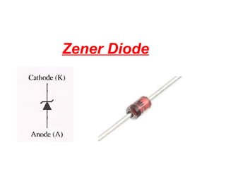
SlideShare a Scribd company logo
Zener Diode
Outlines
 Introduction of Zener Diode
 Construction of Zener Diode
 Working of Zener Diode
 Application of Zener Diode
 Numerical of Zener Diode
Introduction
The zener diode is a silicon pn junction devices that differs from rectifier
diodes because it is designed for operation in the reverse-breakdown
region. The breakdown voltage of a zener diode is set by carefully
controlling the level during manufacture. The basic function of zener
diode is to maintain a specific voltage across it’s terminals within given
limits of line or load change. Typically it is used for providing a stable
reference voltage for use in power supplies and other equipment.
Construction of Zener
Zener diodes are designed to operate in reverse breakdown. Two types of reverse
breakdown in a zener diode are avalanche and zener. The avalanche break down
occurs in both rectifier and zener diodes at a sufficiently high reverse voltage. Zener
breakdown occurs in a zener diode at low reverse voltages.
A zener diode is heavily doped to reduced the breakdown voltage.
This causes a very thin depletion region.
The zener diodes breakdown characteristics are determined by the
doping process
Zeners are commercially available with voltage breakdowns of 1.8 V
to 200 V.
Working of Zener
A zener diode is much like a normal diode. The exception being is that it
is placed in the circuit in reverse bias and operates in reverse breakdown.
This typical characteristic curve illustrates the operating range for a zener.
Note that it’s forward characteristics are just like a normal diode.
Breakdown Characteristics
Figure shows the reverse portion of a zener diode’s characteristic
curve. As the reverse voltage (VR) is increased, the reverse current (IR)
remains extremely small up to the “knee” of the curve. The reverse
current is also called the zener current, IZ. At this point, the breakdown
effect begins; the internal zener resistance, also called zener impedance
(ZZ), begins to decrease as reverse current increases rapidly.
ZENER BREAKDOWN
• Zener and avalanche effects are responsible
for such a dramatic increase in the value of
current at the breakdown voltage.
• If the impurity concentration is very high, then
the width of depletion region is very less.
Less width of depletion region will cause high
intensity of electric field to develop in the
depletion region at low voltages.
• Lets take an example to understand things
clearly.
• Let say the width of depletion region is
200 Å (very small). If a reverse bias
voltage of just 4 V is applied to the diode,
then the electric field intensity in the
depletion region will be
4 = 2 x 10⁸
V/m
200 x 10-10
.
• Merely a voltage of 4 V is responsible to generate
an electric field intensity of 2 x 10⁸ V/m (very high
intensity).
• This electric field is sufficient to rupture the bonds
and separate the valence electrons from their
respective nuclei.
• Large number of electrons gets separated from
their atoms, resulting in sudden increase in the
value of reverse current.
• This explanation was given by scientist C. E.
Zener. Such diodes are called Zener diodes.
• Zener effect predominates in diodes whose
breakdown voltage is below 6 V.
AVALANCHE BEAKDOWN
• Zener effect predominates on diodes whose
breakdown voltage is below 6 V. The breakdown
voltage can be obtained at a large value by reducing
the concentration of impurity atom.
• We know that very little amount of current flows in
the reverse biased diode. This current is due to the
flow of minority charge carriers i.e., electrons in the
p type semiconductor and holes in the n type
semiconductor.
.
• The width of depletion region is large when the
impurity concentration is less.
• When a reverse bias voltage is applied across the
terminals of the diode, the electrons from the p type
material and holes from the n-type materials
accelerates through the depletion region.
• This results in collision of intrinsic particles
(electrons and holes) with the bound electrons in the
depletion region. With the increase in reverse bias
voltage the acceleration of electrons and holes also
increases.
• Now the intrinsic particles collides with bound
electrons with enough energy to break its covalent
bond and create an electron-hole pair. This is shown
in the figure.
Avalanche Breakdown
Mechanism
.
• The collision of electrons with the atom creates an
electron-hole pair.
• This newly created electron also gets accelerated
due to electric field and breaks many more
covalent bond to further create more electron-hole
pair.
• This process keeps on repeating and it is
called carrier multiplication.
• The newly created electrons and holes contribute
to the rise in reverse current.
• The process of carrier multiplication occurs very
quickly and in very large numbers that there is
apparently an avalanche of charge carriers.
Thus the breakdown is called avalanche
breakdown.
DIFFERENCE BETWEEN ZENER
AND AVALANCHE BREAKDOWN
Zener Breakdown
1.This occurs at junctions which being
heavily doped have narrow depletion
layers
2. This breakdown voltage sets a
very strong electric field across
this narrow layer.
3. Here electric field is very strong
to rupture the covalent bonds
thereby generating electron-hole
pairs. So even a small increase in
reverse voltage is capable of producing
Large number of current carriers.
4. Zener diode exhibits negative temp:
coefficient. Ie. breakdown voltage
decreases as temperature increases.
Avalanche breakdown
1. This occurs at junctions which
being lightly doped have wide depletion layers.
2. Here electric field is not strong
enough to produce Zener breakdown.
3. Her minority carriers collide with semi
conductor atoms in the depletion region, which
breaks the covalent bonds and electron-hole
pairs are generated. Newly generated charge
carriers are accelerated by the electric field
which results in more collision and generates
avalanche of charge carriers. This results in
avalanche breakdown.
4. Avalanche diodes exhibits positive temp:
coefficient. i.e breakdown voltage increases
with increase in temperature.
Zenerdiode
Zener diode Data Sheet Information
VZ: zener voltage
IZT: zener test current
ZZT: zener Impedance
IZK: zener knee
current IZM: maximum
zener current
Ideal Model & Ideal Characteristic Curve of Zener Diode
Practical Model & Ideal Characteristic Curve of Zener Diode
Zener Diode Applications –
Zener Regulation with a Varying Input Voltage
Zener Limiting
Zener diodes can used in ac applications to limit voltage swings to
desired levels.
VZ: zener voltage
Vd: Diode voltage
Vd = 0.7
Numerical of Zener Diode
A zener diode exhibits a certain change in V z for a certain
change in lz on a portion of the linear characteristic curve
between IZK and IZM as illustrated in Figure. What is the zener
impedance?
Temperature Coefficient
• The temperature coefficient specifies the percent change
in zener voltage for each degree centigrade change in
temperature.
• For example, a 12 V zener diode with a positive
temperature coefficient of 0.01% /O
C will exhibit a 1.2 mV
increase in Vz when the junction temperature increases
one degree centigrade.
• The formula for calculating the change in zener voltage
for a given junction temperature change, for a specified
temperature coefficient, is
Where Vz is nominal zener voltage at 250
C. When temp.
coefficient is expressed in mV/0
C
Zenerdiode
Example
• A 5.0V stabilised power supply is 
required  to  be  produced  from 
a 12V DC  power  supply  input 
source. 
The maximum power rating Pz of 
the  zener  diode  is 2W. 
Using  the  zener  regulator  circuit 
calculate:
a)  The  maximum  current  flowing 
through  the  zener  diode. 
b)  The  value  of  the  series 
resistor, Rs
c)  The  load  current IL if  a  load 
resistor  of 1kΩ is  connected 
across  the  Zener  diode. 
d)  The  total  supply  current Is
(a)
(b)
(c)
(d)
Zener Diode Voltages
• As well as producing a single stabilised voltage 
output,  zener  diodes  can  also  be  connected 
together  in  series  along  with  normal  silicon 
signal  diodes  to  produce  a  variety  of  different 
reference voltage output values
• The values of the individual Zener diodes can be 
chosen  to  suit  the  application  while  the  silicon 
diode  will  always  drop  about  0.6  -  0.7V  in  the 
forward bias condition. 
• The supply voltage, Vin must of course be higher 
than the largest output reference voltage
Zenerdiode
Summary
• A  zener  diode  is  always  operated  in  its  reverse  biased 
condition. 
• A voltage regulator circuit can be designed using a zener 
diode  to  maintain  a  constant  DC  output  voltage  across 
the  load  in  spite  of  variations  in  the  input  voltage  or 
changes in the load current. 
• The zener voltage regulator consists of a current limiting 
resistor Rs connected in series with the input voltage Vs 
with the zener diode connected in parallel with the load 
RL in this reverse biased condition. 
• The stabilized output voltage is always selected to be the 
same as the breakdown voltage Vz of the diode.

More Related Content

PPTX
Zener doide
PPTX
02 zenerdiodes ppt_prp
PPT
Special purpose diode
DOCX
Zener diode as voltage regulator
PPTX
Zener diode
PPTX
Zener diode and its applications
PPTX
Tunnel Diode
Zener doide
02 zenerdiodes ppt_prp
Special purpose diode
Zener diode as voltage regulator
Zener diode
Zener diode and its applications
Tunnel Diode

What's hot (20)

PPTX
Zener diode 212
PPTX
Zener voltage regulator
PPTX
Zener diode
PDF
Zener diode
PPT
Zener diodes
PPTX
Zener diode as a voltage Regulator
PPTX
Best 3 Applications Involving in Zener Diode Working Functionality
PDF
PPTX
Unijunction transistor (ujt)
PPTX
Semiconductors 101
PPT
Thyristors
PPTX
Zener diode
PPTX
Transistor
PPT
Diodes
PPTX
Zener Diode-As Voltage Regulator
PDF
PPTX
Unsymmetrical fault analysis 2003 final new 2007
PPTX
Presentation1
PPTX
Short channel effects
DOCX
Physics Investigatory:To Study V-I Characteristics Of Zener Diode
Zener diode 212
Zener voltage regulator
Zener diode
Zener diode
Zener diodes
Zener diode as a voltage Regulator
Best 3 Applications Involving in Zener Diode Working Functionality
Unijunction transistor (ujt)
Semiconductors 101
Thyristors
Zener diode
Transistor
Diodes
Zener Diode-As Voltage Regulator
Unsymmetrical fault analysis 2003 final new 2007
Presentation1
Short channel effects
Physics Investigatory:To Study V-I Characteristics Of Zener Diode
Ad

Similar to Zenerdiode (20)

PPTX
Zener Diodes
PPTX
presentatio of electical engineer of topic on problem
DOCX
Informe 4
PPT
Zener Diodes.ppt
PPT
Zenerdiodes
PPTX
Semiconductor diode
PPTX
Zener Diode Introduction and working .pptx
PPTX
Zener Diode Full Presentation
PPTX
Electronic Devices - Special Diodes - Unit 1.pptx
PPT
Chapter 3 special_purpose_diodes Phy.ppt
PPTX
05-Breakdown in PN Diode.pptx
PPTX
Bee Electronic microproject Roll No.41 to 44.pptx
PPTX
ELECTRONICS BY GEEVEE.pptx
PDF
Special Diodes zener, led, photodiode and varactors
PDF
Zener diode experiment.
PPT
10546931.ppt
PPTX
Zenerdiode ppt-111103222100-phpapp02
PPTX
14 Zener Diode 01510515015111201211515.pptx
PDF
V-i characteris (1).pdf
PPTX
Zener diode is useful for voltage regulator.
Zener Diodes
presentatio of electical engineer of topic on problem
Informe 4
Zener Diodes.ppt
Zenerdiodes
Semiconductor diode
Zener Diode Introduction and working .pptx
Zener Diode Full Presentation
Electronic Devices - Special Diodes - Unit 1.pptx
Chapter 3 special_purpose_diodes Phy.ppt
05-Breakdown in PN Diode.pptx
Bee Electronic microproject Roll No.41 to 44.pptx
ELECTRONICS BY GEEVEE.pptx
Special Diodes zener, led, photodiode and varactors
Zener diode experiment.
10546931.ppt
Zenerdiode ppt-111103222100-phpapp02
14 Zener Diode 01510515015111201211515.pptx
V-i characteris (1).pdf
Zener diode is useful for voltage regulator.
Ad

More from Er.Perumal Manimekalai College of Engg (10)

PPTX
Private Profile Company Presentation .pptx
PPTX
Private company tata power limited.pptx
PDF
OCS352 INTERNET OF THINGS notes _Unit -I
PDF
Plc and scada basics and application
PPTX
PPTX
PDF
Armature Leakage reactance
PDF
Basic electrical and electronics engineering
Private Profile Company Presentation .pptx
Private company tata power limited.pptx
OCS352 INTERNET OF THINGS notes _Unit -I
Plc and scada basics and application
Armature Leakage reactance
Basic electrical and electronics engineering

Recently uploaded (20)

PPTX
UNIT-1 - COAL BASED THERMAL POWER PLANTS
PPTX
CH1 Production IntroductoryConcepts.pptx
PPTX
Sustainable Sites - Green Building Construction
PDF
Well-logging-methods_new................
PPTX
MCN 401 KTU-2019-PPE KITS-MODULE 2.pptx
PPTX
M Tech Sem 1 Civil Engineering Environmental Sciences.pptx
PDF
Digital Logic Computer Design lecture notes
PPTX
Geodesy 1.pptx...............................................
PDF
Structs to JSON How Go Powers REST APIs.pdf
PPT
Mechanical Engineering MATERIALS Selection
PPTX
Lesson 3_Tessellation.pptx finite Mathematics
PDF
PPT on Performance Review to get promotions
PDF
Mitigating Risks through Effective Management for Enhancing Organizational Pe...
PDF
SM_6th-Sem__Cse_Internet-of-Things.pdf IOT
PDF
composite construction of structures.pdf
PPTX
OOP with Java - Java Introduction (Basics)
PPTX
Foundation to blockchain - A guide to Blockchain Tech
DOCX
573137875-Attendance-Management-System-original
PDF
July 2025 - Top 10 Read Articles in International Journal of Software Enginee...
PPTX
CARTOGRAPHY AND GEOINFORMATION VISUALIZATION chapter1 NPTE (2).pptx
UNIT-1 - COAL BASED THERMAL POWER PLANTS
CH1 Production IntroductoryConcepts.pptx
Sustainable Sites - Green Building Construction
Well-logging-methods_new................
MCN 401 KTU-2019-PPE KITS-MODULE 2.pptx
M Tech Sem 1 Civil Engineering Environmental Sciences.pptx
Digital Logic Computer Design lecture notes
Geodesy 1.pptx...............................................
Structs to JSON How Go Powers REST APIs.pdf
Mechanical Engineering MATERIALS Selection
Lesson 3_Tessellation.pptx finite Mathematics
PPT on Performance Review to get promotions
Mitigating Risks through Effective Management for Enhancing Organizational Pe...
SM_6th-Sem__Cse_Internet-of-Things.pdf IOT
composite construction of structures.pdf
OOP with Java - Java Introduction (Basics)
Foundation to blockchain - A guide to Blockchain Tech
573137875-Attendance-Management-System-original
July 2025 - Top 10 Read Articles in International Journal of Software Enginee...
CARTOGRAPHY AND GEOINFORMATION VISUALIZATION chapter1 NPTE (2).pptx

Zenerdiode

  • 2. Outlines  Introduction of Zener Diode  Construction of Zener Diode  Working of Zener Diode  Application of Zener Diode  Numerical of Zener Diode
  • 3. Introduction The zener diode is a silicon pn junction devices that differs from rectifier diodes because it is designed for operation in the reverse-breakdown region. The breakdown voltage of a zener diode is set by carefully controlling the level during manufacture. The basic function of zener diode is to maintain a specific voltage across it’s terminals within given limits of line or load change. Typically it is used for providing a stable reference voltage for use in power supplies and other equipment.
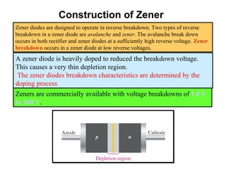
  • 4. Construction of Zener Zener diodes are designed to operate in reverse breakdown. Two types of reverse breakdown in a zener diode are avalanche and zener. The avalanche break down occurs in both rectifier and zener diodes at a sufficiently high reverse voltage. Zener breakdown occurs in a zener diode at low reverse voltages. A zener diode is heavily doped to reduced the breakdown voltage. This causes a very thin depletion region. The zener diodes breakdown characteristics are determined by the doping process Zeners are commercially available with voltage breakdowns of 1.8 V to 200 V.
  • 5. Working of Zener A zener diode is much like a normal diode. The exception being is that it is placed in the circuit in reverse bias and operates in reverse breakdown. This typical characteristic curve illustrates the operating range for a zener. Note that it’s forward characteristics are just like a normal diode.
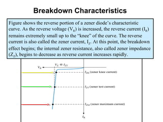
  • 6. Breakdown Characteristics Figure shows the reverse portion of a zener diode’s characteristic curve. As the reverse voltage (VR) is increased, the reverse current (IR) remains extremely small up to the “knee” of the curve. The reverse current is also called the zener current, IZ. At this point, the breakdown effect begins; the internal zener resistance, also called zener impedance (ZZ), begins to decrease as reverse current increases rapidly.
  • 7. ZENER BREAKDOWN • Zener and avalanche effects are responsible for such a dramatic increase in the value of current at the breakdown voltage. • If the impurity concentration is very high, then the width of depletion region is very less. Less width of depletion region will cause high intensity of electric field to develop in the depletion region at low voltages.
  • 8. • Lets take an example to understand things clearly. • Let say the width of depletion region is 200 Å (very small). If a reverse bias voltage of just 4 V is applied to the diode, then the electric field intensity in the depletion region will be 4 = 2 x 10⁸ V/m 200 x 10-10
  • 9. . • Merely a voltage of 4 V is responsible to generate an electric field intensity of 2 x 10⁸ V/m (very high intensity). • This electric field is sufficient to rupture the bonds and separate the valence electrons from their respective nuclei. • Large number of electrons gets separated from their atoms, resulting in sudden increase in the value of reverse current. • This explanation was given by scientist C. E. Zener. Such diodes are called Zener diodes. • Zener effect predominates in diodes whose breakdown voltage is below 6 V.
  • 10. AVALANCHE BEAKDOWN • Zener effect predominates on diodes whose breakdown voltage is below 6 V. The breakdown voltage can be obtained at a large value by reducing the concentration of impurity atom. • We know that very little amount of current flows in the reverse biased diode. This current is due to the flow of minority charge carriers i.e., electrons in the p type semiconductor and holes in the n type semiconductor.
  • 11. . • The width of depletion region is large when the impurity concentration is less. • When a reverse bias voltage is applied across the terminals of the diode, the electrons from the p type material and holes from the n-type materials accelerates through the depletion region. • This results in collision of intrinsic particles (electrons and holes) with the bound electrons in the depletion region. With the increase in reverse bias voltage the acceleration of electrons and holes also increases. • Now the intrinsic particles collides with bound electrons with enough energy to break its covalent bond and create an electron-hole pair. This is shown in the figure.
  • 13. . • The collision of electrons with the atom creates an electron-hole pair. • This newly created electron also gets accelerated due to electric field and breaks many more covalent bond to further create more electron-hole pair. • This process keeps on repeating and it is called carrier multiplication. • The newly created electrons and holes contribute to the rise in reverse current. • The process of carrier multiplication occurs very quickly and in very large numbers that there is apparently an avalanche of charge carriers. Thus the breakdown is called avalanche breakdown.
  • 14. DIFFERENCE BETWEEN ZENER AND AVALANCHE BREAKDOWN Zener Breakdown 1.This occurs at junctions which being heavily doped have narrow depletion layers 2. This breakdown voltage sets a very strong electric field across this narrow layer. 3. Here electric field is very strong to rupture the covalent bonds thereby generating electron-hole pairs. So even a small increase in reverse voltage is capable of producing Large number of current carriers. 4. Zener diode exhibits negative temp: coefficient. Ie. breakdown voltage decreases as temperature increases. Avalanche breakdown 1. This occurs at junctions which being lightly doped have wide depletion layers. 2. Here electric field is not strong enough to produce Zener breakdown. 3. Her minority carriers collide with semi conductor atoms in the depletion region, which breaks the covalent bonds and electron-hole pairs are generated. Newly generated charge carriers are accelerated by the electric field which results in more collision and generates avalanche of charge carriers. This results in avalanche breakdown. 4. Avalanche diodes exhibits positive temp: coefficient. i.e breakdown voltage increases with increase in temperature.
  • 16. Zener diode Data Sheet Information VZ: zener voltage IZT: zener test current ZZT: zener Impedance IZK: zener knee current IZM: maximum zener current
  • 17. Ideal Model & Ideal Characteristic Curve of Zener Diode
  • 18. Practical Model & Ideal Characteristic Curve of Zener Diode
  • 19. Zener Diode Applications – Zener Regulation with a Varying Input Voltage
  • 20. Zener Limiting Zener diodes can used in ac applications to limit voltage swings to desired levels. VZ: zener voltage Vd: Diode voltage Vd = 0.7
  • 22. A zener diode exhibits a certain change in V z for a certain change in lz on a portion of the linear characteristic curve between IZK and IZM as illustrated in Figure. What is the zener impedance?
  • 23. Temperature Coefficient • The temperature coefficient specifies the percent change in zener voltage for each degree centigrade change in temperature. • For example, a 12 V zener diode with a positive temperature coefficient of 0.01% /O C will exhibit a 1.2 mV increase in Vz when the junction temperature increases one degree centigrade. • The formula for calculating the change in zener voltage for a given junction temperature change, for a specified temperature coefficient, is Where Vz is nominal zener voltage at 250 C. When temp. coefficient is expressed in mV/0 C
  • 25. Example • A 5.0V stabilised power supply is  required  to  be  produced  from  a 12V DC  power  supply  input  source.  The maximum power rating Pz of  the  zener  diode  is 2W.  Using  the  zener  regulator  circuit  calculate: a)  The  maximum  current  flowing  through  the  zener  diode.  b)  The  value  of  the  series  resistor, Rs c)  The  load  current IL if  a  load  resistor  of 1kΩ is  connected  across  the  Zener  diode.  d)  The  total  supply  current Is
  • 27. Zener Diode Voltages • As well as producing a single stabilised voltage  output,  zener  diodes  can  also  be  connected  together  in  series  along  with  normal  silicon  signal  diodes  to  produce  a  variety  of  different  reference voltage output values • The values of the individual Zener diodes can be  chosen  to  suit  the  application  while  the  silicon  diode  will  always  drop  about  0.6  -  0.7V  in  the  forward bias condition.  • The supply voltage, Vin must of course be higher  than the largest output reference voltage
  • 29. Summary • A  zener  diode  is  always  operated  in  its  reverse  biased  condition.  • A voltage regulator circuit can be designed using a zener  diode  to  maintain  a  constant  DC  output  voltage  across  the  load  in  spite  of  variations  in  the  input  voltage  or  changes in the load current.  • The zener voltage regulator consists of a current limiting  resistor Rs connected in series with the input voltage Vs  with the zener diode connected in parallel with the load  RL in this reverse biased condition.  • The stabilized output voltage is always selected to be the  same as the breakdown voltage Vz of the diode.