


![State Bubble
Name
[Value]
Output
[Conditional]
State
(transition)](https://image.slidesharecdn.com/05chapter678-sequential-design-231105231413-cccd0726/85/05_Chapter-6-7-8-Sequential-design-ppt-23-320.jpg)


05_Chapter 6,7,8 - Sequential-design.ppt
- 2. Types of Logic Circuits Logic circuits can be: Combinational Logic Circuits-outputs depend only on current inputs Sequential Logic Circuits-outputs depends not only on current inputs but also on the past sequence of inputs
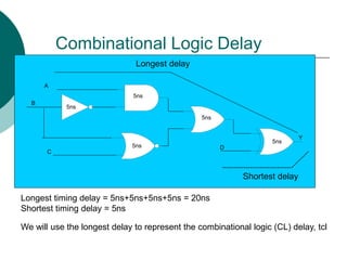
- 4. Combinational Logic Delay A B C D Y 5ns 5ns 5ns 5ns 5ns Shortest delay Longest delay Longest timing delay = 5ns+5ns+5ns+5ns = 20ns Shortest timing delay = 5ns We will use the longest delay to represent the combinational logic (CL) delay, tcl
- 5. Combinational Logic (CL) Cloud Model A B C D E Y 5ns 5ns 5ns 5ns 5ns CL tcl Tcl=20ns Tcl=20ns
- 6. Memory
- 7. Memory We will add memory (or registers) to our logic circuits. This will allow us to design sequential circuits.
- 8. Registers We will represent registers with the following block diagram R E G ps ns clock reset Clock and reset are control signals Ns and ps are data signals
- 10. Sequential Systems General Block Diagram R E G CL F CL H Y ps ns X clock reset Input Vector Output Vector Next State Present State Feedback Path CL= Combinational Logic Cloud Reg= D Registers Clock Reset
- 11. Sequential Systems General Block Diagram R E G CL F CL H Y ps ns X clock reset Input Vector Output Vector Next State Present State Feedback Path Clock Reset X is the input data vector Y is the output data vector
- 12. Sequential Systems Block Diagram R E G CL F CL H Y ps ns X clock reset Input Vector Output Vector Next State Present State Feedback Path Clock Reset Ns is the next state data vector Ps is the present state data vector
- 13. Sequential Systems Block Diagram R E G CL F CL H Y ps ns X clock reset Input Vector Output Vector Next State Present State Feedback Path Clock Reset Notice we have a feedback path which combines the ps data vector with the input vector to generate a new ns data vector.
- 14. Sequential Systems Block Diagram R E G CL F CL H Y ps ns X clock reset Input Vector Output Vector Next State Present State Feedback Path Clock Reset , s s s n F X p Y H p Mathematically, we say Or, ns is a function F of X and ps and Y is a function H of ps.
- 15. Example Circuit Schematic F Logic Register H Logic (buffer) R E G CL F CL H Y ps ns X clock reset X input ns ps Block Diagram
- 16. Example Circuit Schematic F Logic Register H Logic (buffer) X input ns ps State Equations s s s s n J p K p Y p
- 17. Finite State Machine (FSM) General Models
- 18. Moore FSM General Block Diagram R E G CL F CL H Y ps ns X clock reset Input Vector Output Vector Next State Present State Feedback Path CL= Combinational Logic Cloud Reg= D Registers Clock Reset
- 19. Moore FSM State Equations R E G CL F CL H Y ps ns X clock reset Input Vector Output Vector Next State Present State Feedback Path Clock Reset , s s s n F X p Y H p State Equations
- 20. R E G CL F CL H Y ps ns X clock reset Mealy FSM Block Diagram and State Equations , , s s s n F X p Y H X p Input Vector Output Vector Next State Present State Feedback Path Output Y is also a function of input X
- 21. R E G CL F CL H1 Y1 ps ns X clock reset Y2 CL H2 Mealy-Moore FSM Block Diagram and State Equations 1 1 2 2 , , s s s s n F X p Y H X p Y H p Input Vector Next State Present State Mealy Outputs Moore Outputs
- 22. State Diagrams
- 24. State Bubble Example S0 00 Y=0 upn upn Unconditional Transition State name = S0 State value = 00 Y = 0 for this state Conditional Transition We leave this state if upn=1, We remain in this state if upn=0
- 25. Memory Devices
- 26. Memory Devices Data Latch (D-latch) Flip-flops (edge triggered) D-FF, D Register JK-FF T-FF
- 27. D-FF Positive Edge Triggered Block Diagram Q Q SET CLR D Qn+1 D Clk Pre Rst Symbol 4 inputs: D,Clk,Pre,Rst One output: Q D = Data Input Clk = Clock Input Pre = Preset Input Rst = Reset Input
- 28. D-FF Truth Table Q Q SET CLR D Qn+1 D Clk Pre Rst D Clk d d 1 0 0 d d 0 1 1 d 0 1 1 d 1 1 1 0 1 1 0 1 1 1 1 Symbol Equation (rising clock) Truth Table Pre Rst 1 n Q n Q n Q 1 n n Q D
- 29. D-FF Truth Table Q Q SET CLR D Qn+1 D Clk Pre Rst D Clk d d 1 0 0 d d 0 1 1 d 0 1 1 d 1 1 1 0 1 1 0 1 1 1 1 Symbol Equation (rising clock) Truth Table Pre Rst 1 n Q n Q n Q 1 n n Q D Pre= Preset Input (active low) Rst = Reset Input (active low) Highest priority
- 30. D-FF Truth Table Q Q SET CLR D Qn+1 D Clk Pre Rst D Clk d d 1 0 0 d d 0 1 1 d 0 1 1 d 1 1 1 0 1 1 0 1 1 1 1 Symbol Equation (rising clock) Truth Table Pre Rst 1 n Q n Q n Q 1 n n Q D D = Data Input Clk = Clock input Qn = Register Output
- 31. FSM Examples
- 32. Example– 2-bit Up Counter State Diagram S0 s3 S2 S1 Reset Y=0 Y=1 Y=2 Y=3 Clock is implied
- 33. Example – 2-bit Up Counter State Table ps ns y S0 S1 0 S1 S2 1 S2 S3 2 S3 S0 3 S0 = 00 S1 = 01 S2 = 10 S3 = 11 Let Let S0 = reset state State Value Assignment Output Vector
- 34. Example – 2-bit Up Counter Truth Table ps1 ps0 ns1 ns0 y1 y0 0 0 0 1 0 0 0 1 1 0 0 1 1 0 1 1 1 0 1 1 0 0 1 1
- 35. Example – 2-bit Up Counter Excitation Equations 1 1 0 0 0 1 1 0 0 s s s s s s s n p p n p Y p Y p
- 36. Moore FSM R E G CL F CL H Y ps ns X clock reset Input Vector Output Vector Next State Present State Feedback Path Clock Reset , s s s n F X p Y H p State Equations
- 37. Logic Diagram F Logic H Logic Reg Block Y Vector No X Vector in this Example No H Logic needed
- 38. Logic Diagram
- 39. Flash Animation
- 40. Example 3– 2-bit Down Counter State Diagram S0 s3 S2 S1 Reset Y=0 Y=1 Y=2 Y=3 Clock is implied
- 41. Example – 2-bit Down Counter State Table ps ns y S0 S3 0 S3 S2 3 S2 S1 2 S1 S0 1 S0 = 00 S1 = 01 S2 = 10 S3 = 11 Let Let S0 = reset state
- 42. Example – 2-bit Down Counter Truth Table ps1 ps0 ns1 ns0 y1 y0 0 0 1 1 0 0 0 1 0 0 0 1 1 0 0 1 1 0 1 1 1 0 1 1
- 43. Example – 2-bit Down Counter Excitation Equations 1 1 0 0 0 1 1 0 0 s s s s s s s n p p n p Y p Y p
- 44. Recall Moore FSM R E G CL F CL H Y ps ns X clock reset Input Vector Output Vector Next State Present State Feedback Path Clock Reset , s s s n F X p Y H p State Equations
- 45. Logic Diagram F Logic H Logic Reg Block Y Vector No X Vector in this Example
- 46. Logic Diagram
- 47. Example 4 – 2-bit Up/Down Counter State Diagram S0 s3 S2 S1 Reset upn upn upn upn upn upn upn upn
- 48. Example – 2-bit Up/Down Counter State Diagram S0 s3 S2 S1 Reset upn upn Shorthand Notation
- 49. Example – 2-bit Up/Down Counter State Table ps ns upn ns upn y S0 S1 S3 0 S1 S2 S0 1 S2 S3 S1 2 S3 S0 S2 3 S0 = 00 S1 = 01 S2 = 10 S3 = 11 Let Let S0 = reset state
- 50. Example – 2-bit Up/Down Counter Truth Table upn ps1 ps0 ns1 ns0 y1 y0 0 0 0 0 1 0 0 0 0 1 1 0 0 1 0 1 0 1 1 1 0 0 1 1 0 0 1 1 1 0 0 1 1 0 0 1 0 1 0 0 0 1 1 1 0 0 1 1 0 1 1 1 1 0 1 1
- 51. Example – 2-bit Up/Down Counter Excitation Equations 1 1 0 0 0 1 1 0 0 s s s s s s s n p p upn n p Y p Y p
- 52. Recall Moore FSM R E G CL F CL H Y ps ns X clock reset Input Vector Output Vector Next State Present State Feedback Path Clock Reset , s s s n F X p Y H p State Equations
- 53. Logic Diagram X Vector Y Vector F Logic H Logic Reg Block
- 54. Logic Diagram
- 55. Example 5– 3-bit Arbitrary Counter Design a 3-bit arbitrary counter that will count in the following sequence 3,2,3,1,2,3 If a state is not used reset it to state zero. • How may states do we have? • How many registers do we need? • How many bits do we need for Y?
- 56. Example 5– 3-bit Arbitrary Counter State Diagram S0 s3 S2 S1 Reset Y=3 Y=2 Y=3 Y=1 s4 Y=2 S5 S6 S7 Y=0
- 57. Example – Arbitrary 3-bit Counter State Table ps ns y S0 S1 3 S1 S2 2 S2 S3 3 S3 S4 1 S4 S0 2 S5 S0 0 S6 S0 0 S7 S0 0 S0 = 000 S1 = 001 S2 = 010 S3 = 011 S4 = 100 S5 = 101 S6 = 110 S7 = 111 Let Let S0 = reset state Assign State Values
- 58. Develop Truth Table Ps2 Ps1 Ps0 ns2 ns0 ns1 Y Y1 Y0 0 0 0 0 0 1 3 1 1 0 0 1 0 1 0 2 1 0 0 1 0 0 1 1 3 1 1 0 1 1 1 0 0 1 0 1 1 0 0 0 0 0 2 1 0 1 0 1 0 0 0 0 0 0 1 1 0 0 0 0 0 0 0 1 1 1 0 0 0 0 0 0
- 59. Example – 2-bit Arbitrary Counter Develop Excitation Equations -- F Logic 2 2 1 0 1 2 1 0 0 2 0 s s s s s s s s s s s n p p p n p p p n p p
- 60. Develop Excitation Equations for Y 00 01 11 10 0 1 1 1 1 1 00 01 11 10 0 1 1 1 1 Y1 Y0
- 61. Example – 2-bit Arbitrary Counter Excitation Equations -- H Logic 1 2 1 0 1 0 0 2 1 0 s s s s s s s s y p p p p p y p p p
- 62. Recall Moore FSM R E G CL F CL H Y ps ns X clock reset Input Vector Output Vector Next State Present State Feedback Path Clock Reset , s s s n F X p Y H p State Equations
- 64. Logic Circuit
- 65. Simulation
- 66. Example 5– 2-bit Up/Down Counter with Active Low Enable and Synchronous RESET (SRESET) State Diagram Clock is implied S0 s3 S2 S1 Resetn upn en srn en srn upn en srn en srn en srn upn en srn upn en srn srn upn en srn upn en srn srn upn en srn upn en srn en srn
- 67. Example – 2-bit Up/Down Counter with Enable and SRESET Functional Table srn en upn Function 0 d d Synchronous Reset (sreset) 1 1 d Hold 1 0 0 Count Up 1 0 1 Count Down Highest Level of Priority Lowest Level of Priority
- 68. State Table Srn En up n ns 0 d d S0 1 1 d ps 1 0 0 ps+1 1 0 1 ps -1
- 69. Truth Table (5 variables!!) Srn En Upn Ps1 Ps0 Ns0 Ns1 # of Rows 0 d d d d 0 0 16 1 1 d Ps1 Ps0 Ps1 Ps0 8 1 0 0 0 0 0 1 1 1 0 0 0 1 1 0 1 1 0 0 1 0 1 1 1 1 0 0 1 1 0 0 1 1 0 1 0 0 1 1 1 1 0 1 0 1 0 0 1 1 0 1 1 0 0 1 1 1 0 1 1 1 1 1 1 32 Although, we could design this circuit directly from the truth table we will use design partitioning.
- 70. Moore FSM Architecture R E G CL F CL H Y ps ns X clock reset Input Vector Output Vector Next State Present State Feedback Path , s s s n F X p Y H p
- 71. Partitioned Design Mux Y MUX A 2 A 1 A 0 A 3 S1 R E G CL H Y ps ns clock en S0 srn "0" "0" ps reset UP/Down Logic Upn Note, with the partitioned design we can “reuse” already designed submodules to create the “new” design. Srn En ns 0 d S0 1 1 PS 1 0 Count We have srn en
- 72. Top Level Block Diagram
- 75. 2 Bit 4x1 Mux Symbol Circuit
- 76. 1-bit 4x1 Mux Symbol Logic Circuit
- 77. 1-bit 2x1 Mux Symbol Logic Circuit
- 78. Top Level Block Diagram
- 79. Simulation
- 80. Example 6 – FSM Controller State Diagram S0 S1 S2 S3 reset=0 T T T 3 2 1 0 T
- 81. Truth Table for NS Ps1 Ps0 T NS1 Ns0 Y1 Y0 0 0 0 0 1 0 0 0 0 1 0 1 0 0 0 1 0 1 0 0 1 0 1 1 0 1 0 1 1 0 0 1 1 1 0 1 0 1 0 0 1 0 1 1 0 1 0 1 1 1 1 1 1 0 1 1 Truth Table S0 S1 S2 S3 reset=0 T T T 3 2 1 0 T
- 82. Kmaps for NS1 and NS0 P1P0 T 00 01 11 10 0 1 1 1 1 1 NS1 1 0 1 1 0 s s s s ns T p T p p p P1P0 T 00 01 11 10 0 1 1 1 1 1 NS0 0 1 0 1 0 s s s s ns T p T p p p
- 83. Truth Table and Equations for Y Ps1 Ps0 Y1 Y0 0 0 0 0 0 1 0 1 1 0 1 0 1 1 1 1 Truth Table 1 1 0 0 ; Y PS Y PS By Inspection Recall, Moore FSM, so Y will Not be a function of T
- 85. Simulation
- 86. Memory Devices
- 87. Flip-Flops
- 88. D-FF Truth Table Qn follows D on Rising Edge of CLK Q Q SET CLR D Qn+1 D Clk Pre Rst D Clk d d 1 0 0 d d 0 1 1 d 0 1 1 d 1 1 1 0 1 1 0 1 1 1 1 Symbol Equation (rising clock) Truth Table Pre Rst 1 n Q n Q n Q 1 n n Q D D = Data Input Clk = Clock input Qn = Register Output
- 89. T-FF (Toggle) Changes state on every tick of CLK T Clk D d 1 0 0 D d 0 1 1 d 0 1 1 d 1 1 1 0 1 1 1 1 1 Symbol Equation (rising clock) Truth Table Pre Rst 1 n Q n Q n Q 1 n n n Q TQ TQ T Clk Pre Rst Q Q SET CL R T Qn+1 n Q n Q
- 90. SR-FF Set =>Qn=1 Reset=>Qn=0 S R Clk d d d 1 0 0 d d d 0 1 1 d d 0 1 1 d d 1 1 1 0 0 1 1 0 1 1 1 0 1 0 1 1 1 1 1 1 1 ??? n Q Symbol Equation (rising clock) Truth Table Pre Rst 1 n Q n Q n Q Rst Q Q SET CLR S R S Clk R Pre Qn+1 1 n n Q SRQ SR
- 91. JK-FF J K Clk d d d 1 0 0 d d d 0 1 1 d d 0 1 1 d d 1 1 1 0 0 1 1 0 1 1 1 0 1 0 1 1 1 1 1 1 1 n Q Symbol Equation (rising clock) Truth Table Pre Rst 1 n Q n Q 1 n n n Q JQ KQ n Q n Q Rst J Q Q K SET CLR J Clk K Pre Qn+1
- 92. Example: Design a JK-FF using only Logic and a D-FF J K Clk d d d 1 0 0 d d d 0 1 1 d d 0 1 1 d d 1 1 1 0 0 1 1 0 1 1 1 0 1 0 1 1 1 1 1 1 1 n Q Symbol Truth Table Pre Rst 1 n Q n Q n Q n Q Rst J Q Q K SET CLR J Clk K Pre Qn+1
- 93. Example S0 S1 Reset 0 1 J K J K J K PS NS Y 0 0 S0 S0 0 0 0 S1 S1 1 0 1 S0 S0 0 0 1 S1 S0 1 1 0 S0 S1 0 1 0 S1 S1 1 1 1 S0 S1 0 1 1 S1 S0 1 State Diagram State Table Let s0=0 and s1=1
- 94. JK-FF J K PS NS Y 0 0 0 0 0 0 0 1 1 1 0 1 0 0 0 0 1 1 0 1 1 0 0 1 0 1 0 1 1 1 1 1 0 1 0 1 1 1 0 1 Truth Table s s s s n J p K p Y p Logic Equations
- 95. Recall Moore FSM State Equations R E G CL F CL H Y ps ns X clock reset Input Vector Output Vector Next State Present State Feedback Path Clock Reset , s s s n F X p Y H p State Equations
- 96. JK Example Circuit Schematic F Logic D-Register H Logic (buffer) R E G CL F CL H Y ps ns X clock reset X input ns ps Block Diagram
- 97. JK Example Circuit Schematic Simulation
- 98. Latches
- 99. D-Latch Block Diagram Symbol D E Pre Rst Q Q SET CLR D E Qn+1 4 inputs: D,E,Pre,Rst One output: Q D = Data Input E = Enable Input Pre = Preset Input Rst = Reset Input
- 100. D-Latch Truth Table D E d d 1 0 0 d d 0 1 1 d 0 1 1 0 1 1 1 0 1 1 1 1 1 Symbol Truth Table Pre Rst 1 n Q n Q D E Pre Rst Q Q SET CLR D E Qn+1
- 101. D-Latch State Equations D E d d 1 0 0 d d 0 1 1 d 0 1 1 0 1 1 1 0 1 1 1 1 1 Symbol Equation (level clock) Truth Table Pre Rst 1 n Q n Q 1 n n n Q EQ ED D E Pre Rst Q Q SET CLR D E Qn+1
- 102. SR-Latch State Equations S R d d 1 0 0 d d 0 1 1 0 0 1 1 0 1 1 1 0 1 0 1 1 1 1 1 1 1 ??? Symbol Equation (level clock) Truth Table Pre Rst 1 n Q n Q 1 n n Q SRQ SR S R Pre Rst Q Q SET CLR S R Qn+1
- 104. Simulation
- 106. Shift Registers Logic Design which manipulates the bit position of binary data by shifting it to the left or right. Major application Serial Data to Parallel Data converters
- 107. Example Design a three-bit shift register with the following functions S1 S0 Function 0 0 Synchronous Reset (sreset) 0 1 Shift Right 1 0 Shift Left 1 1 No Shift
- 109. No Shift Equations and Circuit 2 2 1 1 0 0 s s s s s s n p n p n p
- 110. Shift Left Equations and Circuit 2 1 1 0 0 2 s s s s s s n p n p n p Shift Left ps ns
- 111. Shift Right Equations and Circuit 2 0 1 2 0 1 s s s s s s n p n p n p Shift Right ps ns
- 113. Registers
- 114. Total Design