


AE UNIT IV.ppt
- 1. UNIT IV FIELD CONTROLLED DEVICES ANALOG ELECTRONS
- 2. Classification of Transistor Two types of transistor as Unipolar junction transistor Current conduction due to only majority carrier. Commonly known as FET. It is voltage operated devices FET can classified as Junction Field Effect Transistor (JFET) Metal Oxide Semiconductor FET (MOSFET) Metal semiconductor FET (MESFET) Biploar junction transistor Current conduction due to both holes and electrons. It is current operated devices and classified as npn, pnp
- 3. FIELD EFFECT TRANSISTOR (FET) BJT is current controlled devices JFET is voltage controlled devices Voltage is applied then control the electric field created. So name called as Field Effect Transistor BJT is bipolar device which control conduction by both charge carrier FET is unipolar device which control conduction by either charge carrier (electrons and holes). FET is a high i/p impedance.
- 4. Types of FET
- 6. Consist of 2-PN junction form opposite side of its middle part. Space between junction called channel or bar If bar is N-type then n-Channel JFET. Similarly for p- Channel JFET. Where forming pn junction taken gate(G) terminal in single wire. Both end of bars taken from drain(D) and source (S) Where source and drain enters majority carriers VGS applied reverse such that make R.B of PN junction. Majority carrier moves from source to drain via channel Symbol In n-channel JFET arrow mark enters towards the vertical line. Vertical line represents channel.
- 7. Operation of JFET VGS=0V, VDS some +ve value
- 8. Initially two depletion region width touch (but not actually meet) this condition referred as pinch off. VDS ↑, then establish this condition and corresponding voltage as pinch off voltage (Vp) Here prevent high electric field due to depletion region. VDS >Vp, then region between two depletion layer will increases along the channel. But ID level remains same. Here JFET act as current source (ID=IDSS) but voltage find based on loading
- 9. Operation when VGS<0V •VGS is controlled voltage of JFET. Which is more negative •Apply VDS when electrons drawn to drain terminal •ID=IS •Flow of charge in channel is limited by resistance of channel •VDS ↑, c.s area of channel ↓ by increase depletion region on top of p-type layer. Here apply more R.B •VDS ↑, then current ↑ •When VDS=Vp, then wider depletion region and causes to decrease the channel width. So R increase and so curve is slightly bending.
- 10. If VGS become –ve, then apply R.B. So depletion width ↑ still. Need less VDS to occurs pinch off When VGS=-Vp then device will be turn off. VDS ↑ sufficiently large then avalanche breakdown in pinch off region and ID ↑ Region in left of pinch off referred as ohmic or voltage controlled resistance region In this region JFET act as variable resistance which controlled by VGS VGS become more –ve then slope of each curve becomes horizontal
- 11. JFET Characteristics There is a two characteristics as Drain characteristics Transfer characteristics Drain characteristics Plot ID Vs VDS at different values of VGS
- 12. Cut-off region VGS ↑ -vely, channel width ↓ At certain voltage VGS(off), depletion region completely close the channel So ID=0, when VGS>VGS(off) Saturation region The portion where ID remains const. Here FET use as an amplifier Ohmic region ID varies w.r.to VDS. FET operates as voltage variable resistance. R ↓, when –ve VGS↓ Breakdown region Here VDS>Vp, then ID=const, upto certain values of VDS. VDS ↑ still, then B.D gate channel junction due to avalanche effect.
- 13. Transfer characteristics Indicate relationship between ID and VGS Curve obtained by using Shockley equation Operating limit of JFET as When VGS=0V, ID=IDSS When VGS=Vp, ID=0mA
- 14. Characteristics
- 15. Characteristics parameter of JFET Mutual conductance or transconductance, gm Its unit is mho. Drain resistance, rd Its unit is ohms Amplification factor, µ
- 16. P-Channel JFET Its construction is same manner but reversal of p and n-type material.
- 17. Here reversing the polarity of ID, VGS,VDS ID flows due to holes. ID↑, -ve VDS↑ VGS is +ve, VGS ↑ then ID↓ due to reduction of channel width. In symbol arrow head flows out off vertical line
- 18. Drain Characteristics Here same shape of n-channel JFET but polarity of VGS and VDS reversed
- 20. Comparison of JFET and BJT S.No JFET BJT 1 Operates only on flow of majority carrier. So called Unipolar devices Operates both of majority minority carrier. 2 It has no junction. Conduction through N-type and P-type material. It have junction and noisy 3 If i/p circuit is R.B, then establish higher i/p impedance and low o/p impedance. JFET act as buffer amplifier. It have low i/p impedance due to F.B in i/p side. 4 It is voltage controlled device It is current controlled device. 5 It tolarate higher level of radiation due to no minority carrier. Performance is degraded due to neutron radiation because reduction in minority carrier lifetime. 6 Easy to fabricate in ICs Size is big compare to JFET 7 It prevent thermal B.D due to have –ve temperature coefficient at high current It is possible to thermal B.D due to have +ve temperature coefficient at high current 8 It have higher switching speed and cut- off frequency due to not suffer minority carrier storage. It have lower switching speed and cut-off frequency due to problem of minority carrier storage.
- 21. Application of JFET Used as buffer in measuring instruments, receivers since it have high i/p impedance and low o/p impedance Used in RF amplifier in FM tuners and communication equipment for low noise level. Used in cascade amplifiers in measuring and testing equipments. Use as voltage variable resistor in op-amp Use as mixer circuit in FM and TV receivers and communication equipment because inter modulation distortion is low. Used in oscillator circuit Due to low coupling capacitor it used in low frequency amplifiers in hearing sida and inductive transducer
- 22. FIELD EFFECT TRANSISTOR (MOSFET) Commonly as IGFET- Insulated Gate Field Effect Transistor Types as Enhanced MOSFET By controlling electric field cause to increase majority carrier density in conducting region. Here absent n-channel. Depletion MOSFET By controlling electric field cause to reduce the minority carrier density in conducting region. Here n-channel is present. Principle By applying a transerve electric field across insulator, deposited in semiconductor material, thickness and hence the resistance of a conducting channel of a semi conductor material can be controlled.
- 23. n-Channel depletion MOSFET Construction as shown
- 24. n+ region has highly doping and p-type substrate has lightly doped. n+ region diffused into p-type substrate. S & D taken from n+ region SiO2 insulating layer grown on surface and cut in small place where S & D placing. Thin layer of metal Al placed over SiO2 (shown in black colour) G is formed in metal Al layer. SiO2 layer opposing externally applied electric field n-channel diffused between S & D
- 25. Operation and characteristics n-channel depletion MOSFET with VGS=0V and applied voltage VDD as shown
- 26. Reduction of free carriers in a channel due to a –ve potential at gate terminal as shown Set VGS=0V and apply VDS. Here attract +ve charge to D-terminal. When VGS=0V, then ID=IDSS
- 27. Set VGS=-ve -ve charges in G repels (like charge) electrons in n- channel and attract electrons (opposite charge) in p- substrate. Here indirectly n-channel width ↓ So due to this no free electrons ↓ in n-channel for conduction. More –ve VGS apply, then ID ↓ When VGS is -ve, then ↓ no of free electrons. So called depletion mode. Set VGS=+ve +ve charges in G attract (opposite charge) electrons in n- channel and attract electrons (opposite charge) in p- substrate. Here indirectly n-channel width ↑ So due to this no free electrons ↑ in n-channel for
- 28. Characteristics
- 29. p-Channel depletion MOSFET Construction as shown This construction has exactly reverse the n- channel. Here channel is p- type and substrate is n-type Operation is same as n-channel but here explain with flow of holes only.
- 30. Transfer characteristics Drain characteristics
- 31. Symbol Symbol reflect construction G- not connected to other terminal, reason that G insulation Vertical line rep as channel which connect between D & S Two symbol rep as some cases substrate is externally available.
- 32. n-Channel Enhancement MOSFET Construction as shown Here there is no physical channel
- 33. n+ region has highly doping and p-type substrate has lightly doped. n+ region diffused into p-type substrate. S & D taken from n+ region SiO2 insulating layer grown on surface and cut in small place where S & D placing. Thin layer of metal Al placed over SiO2 (shown in black colour) G is formed in metal Al layer. SiO2 layer opposing externally applied electric field Cap forms due to metal area of G, SiO2 and p-substrate This device called as Insulated Gate FET due to insulating layer of SiO2. this layer gives high i/p impedance
- 34. Operation and characteristics Channel formation in n-channel enhancement type MOSFET as shown
- 35. Set VGS=0V and apply VDS, then ID=0A due to no n- channel. VGS & VDS ↑ to +ve value, then D & G +ve w.r.to S Holes in G repels (like charges) in p-substrate in edge of SiO2 layer. Forms depletion region near to SiO2 in p –substrate. Electrons (minority carrier) flows from n-region through depletion region. Electrons to the p-substrate attracted to +ve G and accumulate near the surface of SiO2 layer. SiO2 insulating layer prevent the attracted electron in depletion layer VGS ↑, then concentration of electron near the surface of SiO2 layer ↑. VGS=VT (theresold voltage), then ID starts ↑. (i.e) like cut-
- 36. VGS>VT, then density of electrons ↑, so ID level also ↑ Keep VGS=const, VDS ↑, so ID reach sat level due to pinching off process Again VDS ↑ still, but ID =const Change of channel and depletion region with increasing level of VDS for fixed VGS as shown
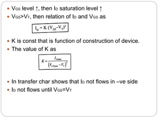
- 37. VGS level ↑, then ID saturation level ↑ VGS>VT, then relation of ID and VGS as K is const that is function of construction of device. The value of K as In transfer char shows that ID not flows in –ve side ID not flows until VGS=VT
- 38. Characteristics of n-channel enhancement MOSFET
- 39. p-Channel Enhancement type MOSFET Here substrate is n-type and p-region where placing S & D. Characteristics are exactly reverse in case of n- channel enhancement type MOSFET
- 40. Drain characteristics ID ↑ with –ve value of VGS Transfer characteristics It mirror image of previous topics
- 41. Symbol Here dashed line indicate that channel not exist.
- 42. Comparison of MOSFET and JFET S.N o MOSFET JFET 1 Electric field across SiO2 insulating layer control the conductivity of channel Electric field across R.B PN junction control the conductivity of channel 2 Gate leakage current= 10^- 12A Rin=10^10 to 10^15Ω Gate leakage current= 10^-9A Rin=10^8 Ω 3 Operate both depletion and enhancement mode Operate only depletion mode 4 Easy to fabricate Difficult to fabricate 5 Source and Drain are interchangeable. Such provision not there.
- 43. MOSFET SMALL SIGNAL MODEL DEPLETION TYPE MOSFETS The ac equivalent model for D-MOSFETs is exactly same as that used for JFET as shown
- 44. ENHANCEMENT TYPE MOSFETS AC small signal equivalent circuit as shown O.C between G & S. Then apply VGS Current source from D & S which depends on VGS The relation between o/p current and controlled voltage as
- 45. gm can be determined by taking derivative of the transfer equation
- 46. Small signal Analysis of E-MOSFET Drain- Feedback Configuration Here i/p fed to G and o/p taken from D The circuit diagram of drain feedback configuration as shown
- 47. AC equivalent model of drain feedback configuration as shown Here capacitor as S.C and deactivate the dc source
- 48. Input impedance (Zi): It calculated from small signal model of the circuit Apply LCL at node D as
- 49. Output impedance (Zo): The o/p impedance can calculated as If Vi=0, then Vi=VGS=0. so current source also zero. This as shown Voltage gain (Av): It is defined as ratio of o/p voltage to i/p voltage
- 50. Apply KCL at node D as -ve sign indicates as Vi and Vo as 180 deg outoff phase
- 51. Small signal analysis of E-MOSFET Voltage –Divider Configuration i/p as fed from---G and o/p taken as from------D For ac analysis S- connected to ground and hence common to both i/p and o/p. Circuit diagram as shown
- 52. AC equivalent network where cap as S.C and deactivate dc source as shown Input impedance (Zi): It is R-looking from i/p terminal (G & S)
- 53. Output impedance (Zo): It is R-looking from o/p terminal (D & S) If Vi=0, VGS=0, then current source also deactivated. This as shown Voltage gain (Av): It is ratio of o/p voltage to i/p voltage The o/p voltage is given as
- 55. UNI JUNCTION TRANSISTOR (UJT) It is 3-terminal Si semiconductor device. It has one PN junction like ordinary diode Construction as shown
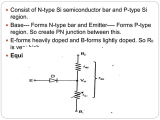
- 56. Consist of N-type Si semiconductor bar and P-type Si region. Base--- Forms N-type bar and Emitter---- Forms P-type region. So create PN junction between this. E-forms heavily doped and B-forms lightly doped. So RB is very high Equivalent circuit as shown
- 57. It consist of diode and resistance. Diode rep as PN junction.rB1 & rB2 rep as N-type bar resistivity. rBB is total resistance of B-terminal. It is called inter base resistance. rBB value= 5 to 10 KΩ, if no voltage applied to UJT. rB1 is variable nature. rB1 α (1/IE), rB1=4KΩ to 40Ω Intrinsic strand-off ratio(η) Here E-open then VBB divides across two resistance
- 58. Voltage across the resistance rB1 as The ratio of rB1/rB2 is known as intrinsic stand-off ratio. V.D across rB1 is called intrinsic stand off voltage. It R.B the emitter side.
- 59. UJT operation V.D across rB1= ηVBB and VD makes R.B of diode. So IE in cut-off region. Total R.B voltage= ηVBB + VD Small leakage current flows from B2 to E due to minority carrier. If VE<(ηVBB + VD), then diode not conduct and IE not flows. If VE exceed so IE flows. The voltage at which diode
- 60. VE reaches Vp, then diode conduct (become F.B). So IE flows and UJT remains turned ON. under this condition, holes injected to N-type bar. Due to excess holes in rB1 ↓. So voltage across it also↓. (i.e) ηVBB. So causes IE ↑. Produces –ve resistance region in V-I char and UJT switches from OFF to ON position. If –ve voltage applied across E-region then UJT not turned ON.
- 61. V-I characteristics of UJT Peak point and valley point is two important point in char. Three important region as: cut-off region, negative resistance region, saturation region.
- 62. Cut-off region It is left of peak point. Here VE<Vp, IE=0A UJT remains OFF. Negative resistance region It is the region between peak point and valley point. VE↓ from Vp to Vv IE ↑ from Ip to Iv IE ↑, then rB1 ↓. So called –ve resistance region. Saturation region It is the region beyond valley point. Device is ON Application •Trigger device for SCR and TR •Non sinusoidal oscillator •Saw tooth generator •Timing circuits
- 63. UJT Relaxation Oscillator It is used to generate saw tooth waveform.
- 64. It consist of UJT Cap charged by VBB via R VC ↑ exponentially and VC reaches to Vp= (ηVBB + VD), then UJT start conducting. Cap discharge to E-B1 and R1. Once cap discharge after reach Vp then provides –ve resistance path to useful of oscillator working. After discharge, VC=0V, then again cap starts charging and cycle repeats. When UJT firing, then sudden surges of VB1 across R1 provides +ve spike. Also generate –ve going spike across R2.
- 65. Frequency of Oscillation Change in value of C or R, then control freq, this can be controlling by time constant RC. First calculate time period and then getting frequency.