SlideShare a Scribd company logo
Microprocessor and Micro Controller
Unit II
8085 Pinout Signal, Functional Block Diagram
and Instruction Set
Prepared By
Dr. S.Murugan, Associate Professor
Department of Computer Science,
AlagappaGovernment Arts College, Karaikudi.
(Affiliated by AlagappaUniversity)
Mailid: muruganjit@gmail.com
Reference Book:
Microprocessor Architecture – Programming and Applications with 8085 – R. S. Gaonkar
8085 Microprocessor Unit (MPU)
The 8085 MPU
➢ The term microprocessing unit (MPU) is similar to
central processing unit (CPU) used in traditional
computers.
➢ The MPU as a device or a group of devices (as a unit)
that can communicate with peripherals, provide timing
signals, direct data flow, and perform computing task
as specified by the instructions in memory.
The 8085 MPU
➢ Limitations of MPU :
➢ The low-order address bus is multiplexed with the
data bus. The buses needed to be demultiplexed.
➢ Appropriate control signals need to be generated to
interface memory and I/O with the 8085 MPU.
The 8085 Microprocessor – Pinout Signal
➢ The 8085A is an 8-bit general-purpose microprocessor
capable of addressing 64K of memory.
➢ The device has 40 pins, requires a +5V single power
supply and can operate with a 3-MHz single phase
clock.
➢ Fig. 2.1 shows the logic pinout diagram of the 8085
microprocessor.
The 8085 Microprocessor – Pinout Signal
➢ All the signals classified into six groups:
➢ 1. Address bus
➢ 2. Data bus
➢ 3. Control and Status Signal
➢ 4. Power supply and frequency signals
➢ 5. Externally initiated signals
➢ 6. Serial I/O ports.
The 8085 Microprocessor – Pinout Signal
Figure 2.1 The 8085 Microprocessor Pinout and Signals
1. Address Bus
➢ The 8085 has 16 signal lines are used as address bus.
➢ These lines are split into two segments: A15 - A8 and
AD7 - AD0.
➢ The eight signal lines, A15-A8 are unidirectional and
used for the most significant bits, called the high-order
address, of a 16-bit address.
➢ The signal lines AD7-AD0 are used for a dual purpose.
2. Multiplexed Address/Data Bus
➢ The signal lines AD7-AD0 are bidirectional .
➢ It is used for a dual purpose, the low-order address
bus as well as data bus.
➢ These lines are enabled by the ALE (address Latch
Enable) signal.
3. Control and Status Signal
➢ It includes two control signals (RD and WR), three
status signals (IO/M. S1 and S0) to identify the nature
of the operations, one special symbol ALE).
➢ ALE – Address Latch Enable : When ALE is high, it
indicates that the bus (AD7-AD0 lines) is carrying an
address. When ALE is low, the bus (AD7-AD0 lines) is
typically used for transferring actual data.
3. Control and Status Signal
➢ RD - Read: This signal indicates that the selected I/O or memory
device is to be read; and data are available on the data bus
➢ WR – Write : This signal indicates that the data on the data bus are
to be written into a selected I/O or Memory
➢ IO/M : This is a control signal that indicates whether the current
operation is related to I/O or memory. When this signal is high, it
indicates an I/O operation. When this signal is low, it indicates a
memory operation
3. Control and Status Signal
➢ S1 and S0 : These are two status lines that indicate the specific type of
machine cycle (fetch, read, write, etc.).
➢ All the operations and their associated status signals are listed in Table
2.1
Table 2.1 8085 Machine Cycle Status and Control Signals
4. Power Supply and Clock Frequency
➢ Vcc : Pin 40 is the Vcc pin that connects to the positive power supply
(typically +5V). Vcc provides the necessary power for the operation of
the microprocessor and its internal circuits.
➢ Vss: Vss is typically connected to the system's ground (0V).
➢ X1, X2 : A crystal is connected to these two pins. The frequency is
internally divided by two; the system operates at 3 MHz. Totally, the
crystal should have a frequency of 6 MHz. The crystal generating a
stable clock signal at a fixed frequency.
➢ CLK (Out) – Clock Output : This signal can be used as the system
clock for other devices.
5. Externally Initiated Signal, Including Interrupts
➢ The 8085 has five interrupt signals that can be used to interrupt a
program execution.
➢ In addition to the interrupts, three pins – RESET, HOLD, and READY
– accept the externally initiated signals as inputs.
➢ The functions of these signals are listed in Table 2.2
5. Externally Initiated Signal, Including Interrupts
Table 2.2 8085 Interrupts and Externally Initiated Signals
5. Externally Initiated Signal, Including Interrupts
➢ RESET IN: When the signal on this pin goes low, the program counter
is set to zero and the MPU is set to zero.
➢ RESET OUT: This signal is used to reset other devices.
6. Serial IO Ports
➢ The 8085 has two signals to implement the serial transmission :
➢ SID (Serial Input Data) and SOD (Serial Output Data).
➢ In serial transmission, data bits are sent over a single line, one bit at a
time.
Functional Block Diagram (A Detailed Look at the 8085 MPU and Its Architecture)
➢ Figure 2.2 shows the internal architecture of the 8085.
➢ It includes the ALU (Arithmetic Logic Unit), Timing and Control Unit,
Instruction Register and Decoder, Register Array, Interrupt Control,
and Serial I/O Control.
Functional Block Diagram - The ALU
➢ The arithmetic/logic unit performs the computing functions: it includes
the accumulator, the temporary registers, the arithmetic and logic
circuits, and five flags.
➢ The temporary register is used to hold data during an arithmetic/logic
operation.
➢ The result is stored in accumulator, and the flags (flip-flops) set or reset
according to the result of the operation.
➢ The flags are generally reflects data condition in the accumulator.
➢ The Bit position, Flag name, description, purpose and example
mnemonic are as follows:
Functional Block Diagram - The ALU – Flag Registers
Bit
Position
Flag Name Description Purpose Example
Mnemonic
7 Sign Flag (S) Set (1) if the result of the operation is
negative (i.e., the most significant bit of the
result is 1), otherwise reset (0).
Indicates if the result of an operation is
negative.
SBB (Subtract
with Borrow)
6 Zero Flag (Z) Set (1) if the result of the operation is zero,
otherwise reset (0).
Indicates if the result of an operation is
zero.
CMP
(Compare)
4 Auxiliary Carry
Flag (AC)
Set (1) if there is a carry from bit 3 to bit 4
during addition or a borrow during
subtraction, otherwise reset (0).
Used in BCD (Binary Coded Decimal)
arithmetic operations.
ADD (Add)
2 Parity Flag (P) Set (1) if the result has an even number of
1's (even parity), otherwise reset (0) for odd
parity.
Indicates whether the result has even or
odd parity.
INX (Increment
register pair)
0 Carry Flag (C) Set (1) if there is a carry-out from the most
significant bit during an addition operation,
or if there is a borrow during a subtraction.
Indicates carry/borrow during
arithmetic operations.
JC (Jump if
Carry)
1, 3, 5 Unused This bit is unused and always set to 0. This bit has no specific function in the
flag register.
N/A
➢ The bit positions reserved for these flags in the flag register are as
follows:
Functional Block Diagram - The ALU – Flag Registers
Functional Block Diagram - Timing and Control Unit
➢ This unit synchronizes all the microprocessor operations with the clock
and generates the control signals necessary for communication between
the microprocessor and peripherals.
➢ The RD and WR signals are sync pulses indicating the availability of
data on the data bus.
Functional Block Diagram - Instruction Register and Decoder
➢ The instruction register and the decoder are part of the ALU.
➢ When an instruction is fetched from memory, it is loaded in the
instruction register.
➢ The decoder decodes the instruction and establishes the sequence of
events to follow.
8085 Instruction Set and Classification
Instruction Set
➢ An instruction is a binary pattern designed inside a microprocessor to
perform a specific function.
➢ The entire group of instructions, called the instruction set, determines
what functions the micro processor can perform.
8085 Instruction Set and Classification
Classification:
➢ The 8085 instructions can be classified into the following five
functional categories:
➢ data transfer operations,
➢ arithmetic operations,
➢ logical operations,
➢ branching operations and
➢ machine control operations.
Instruction Classification - Data Transfer (Copy) Operations
➢ This group of instructions copies data from a location called a source to
another location, called a destination, without modifying the content of
the source.
➢ The various types of data transfer are listed below together with
examples of each type.
Instruction Classification - Data Transfer (Copy) Operations
S.No. Type Examples Mnemonics
1 Between Registers Copy or moves the contents of
register B into Register D.
MOV D,B
2 Specific data byte to a
register or a memory
location
Load Register B with the data
byte 32H.
MVI B, 32
3 Between a memory location
and a register
From the memory location
2000H to Register B
MOV B, 2000
4 Between an I/O device and
the accumulator
From an input keyboard to the
accumulator. Assume the
keyboard connected to I/O port
00H.
IN 00H
Instruction Classification – Arithmetic Operations
➢ These instructions perform arithmetic operations like addition,
subtraction, increment, and decrement.
➢ ADD (Add Register or Memory): Adds the content of a register or
memory to the accumulator. The sum is stored in the accumulator.
Example: ADD B (Add the contents of register B to the accumulator).
➢ SUB (Subtract Register or Memory): Subtracts the content of a
register or memory from the accumulator. The result is stored in the
accumulator. Example: SUB C (Subtract the contents of register C
from the accumulator).
Instruction Classification – Arithmetic Operations
➢ INR (Increment Register): Increments the content of a register or
memory by 1. The result is stored in the accumulator.
➢ Example: INR B (Increment the contents of register B by 1).
➢ DCR (Decrement Register): Decrements the content of a register or
memory by 1. The result is stored in the accumulator.
➢ Example: DCR C (Decrement the contents of register C by 1).
Instruction Classification - Logical Operation
➢ These instructions perform various logical operations with the
content of accumulator.
➢ AND, OR, Exclusiove-OR – Any 8-bit number, or the contents of a
register, or of a memory location can be logically ANDed, ORed, or
Exclusive-ORed with the contents of the accumulator. The results are
stored in the accumulator.
➢ Example: ANA B (Perform AND between A and B, and store
the result in A).
➢ Example: ORA B (Perform OR between A and B, and store the
result in A).
➢ Example: XRA C (XOR the contents of register C with A).
Instruction Classification - Logical Operation
➢ Rotate : Each bit in the accumulator can be shifted either left or right
to the next position
➢ RLC: Each binary bit of the accumulator is rotated left by one
position.
➢ RRC: Each binary bit of the accumulator is rotated right by
one position
Instruction Classification - Logical Operation
➢ Compare : Any 8 bit number, or the content of a register, or a
memory location can be compared for equality, greater than, or less
than, with the content of the accumulator.
➢ Complement: The contents of the accumulator can be
complemented; all zeroes are replaced by ones and all ones are
replaced by zeroes.
➢ Example : CMA (Complement the accumulator). If
Accumulator contains the value 06, then the complement of
Accumulator is 249.
Instruction Classification - Branching Operation
➢ These instructions are used to alter the flow of control in the program.
➢ JMP (Jump): Unconditional jump to a specified memory location.
➢ Example: JMP 2050H (Jump to address 2050H).
➢ JC (Jump if Carry): Jump to a specified address if the carry flag is set.
➢ Example: JC 2050H (Jump to 2050H if carry flag is set).
➢ JZ (Jump if Zero): Jump to a specified address if the zero flag is set.
➢ Example: JZ 2050H (Jump to 2050H if zero flag is set).
Instruction Classification - Branching Operation
➢ CALL (Call Subroutine): Calls a subroutine at a specified memory
address.
➢ Example: CALL 3000H (Call subroutine at address 3000H).
➢ RET (Return from Subroutine): Return from a subroutine.
➢ Example: RET (Return from the current subroutine).
Instruction Classification - Machine Control Operations
➢ These instructions control the processor’s execution, such as halting
the program (HLT) or enabling interrupts.

More Related Content

PDF
Lecture Notes - Microprocessor - Unit 1 - Microprocessor Architecture and its...
PPTX
De-Multiplexing of Address and Data Bus in 8086.pptx
PDF
Memory interfacing of microprocessor 8085
PPTX
Register Organisation of 8086 Microprocessor
DOCX
Study of 8051 microcontroller
PPTX
Combinational circuit
PPTX
8086 Microprocessor powerpoint
Lecture Notes - Microprocessor - Unit 1 - Microprocessor Architecture and its...
De-Multiplexing of Address and Data Bus in 8086.pptx
Memory interfacing of microprocessor 8085
Register Organisation of 8086 Microprocessor
Study of 8051 microcontroller
Combinational circuit
8086 Microprocessor powerpoint

What's hot (20)

PPTX
Key board interfacing with 8051
PPTX
Introduction to Microcontroller
PPTX
Flip flops
PDF
8086 modes
PPTX
Minimum mode and Maximum mode Configuration in 8086
PPT
8254-timer.ppt
DOCX
UNIT 1 MSP430.docx
PDF
Interfacing of 8051 with 8255 Programmable Peripheral Interface.pdf
PPTX
Anti bag snatching alarm
PPT
PPTX
Programmable Logic Controller
PPT
8085 microproceesor ppt
PPTX
8086 signals
PDF
Instruction set of 8086
PPT
8086 microprocessor
PPTX
8086 Microprocessor Pipeline Architecture.pptx
PDF
Bus structure of 8085 microprocessor 8085 microprocessor complete tutorial
PPTX
Chapter 7 memory & i/o
PPTX
SAP II ARTICTURE ,SAP 2
Key board interfacing with 8051
Introduction to Microcontroller
Flip flops
8086 modes
Minimum mode and Maximum mode Configuration in 8086
8254-timer.ppt
UNIT 1 MSP430.docx
Interfacing of 8051 with 8255 Programmable Peripheral Interface.pdf
Anti bag snatching alarm
Programmable Logic Controller
8085 microproceesor ppt
8086 signals
Instruction set of 8086
8086 microprocessor
8086 Microprocessor Pipeline Architecture.pptx
Bus structure of 8085 microprocessor 8085 microprocessor complete tutorial
Chapter 7 memory & i/o
SAP II ARTICTURE ,SAP 2
Ad

Similar to Lecture Notes Microprocessor and Controller Unit2 (20)

PPT
8085-microprocessor
PPTX
unit 2 microprocesor8085 for advantages disadvatage gtu syllabus.pptx
PDF
Microprocessor and Microcontroller.pdf
PDF
EEE- BEE603 - Microprocessor and Microcontroller- Mr K Dwarakesh_220819_18121...
PDF
Computer system architecture (microprocessor 8085) unit 4
PPTX
8085 architecture
DOCX
c++
PPTX
PPT 8085 microprocessor
PPT
architect.ppt
PPT
8085.ppt
PPT
8085 intro
PPTX
An introduction to microprocessor architecture using INTEL 8085 as a classic...
PPTX
MICROPROCESSOR AND INTERFACING
PPT
8085 microprocessor Embedded system
PPTX
8085vs8086 microprocessor and their characteristics and functionalities
PPTX
PPT-1.pptx
PPTX
PPT-1.pptx
PDF
8085 microprocessor Architecture and Pin description
PDF
itft-8085 microprocessor
PDF
Unit 2 8085.pdf
8085-microprocessor
unit 2 microprocesor8085 for advantages disadvatage gtu syllabus.pptx
Microprocessor and Microcontroller.pdf
EEE- BEE603 - Microprocessor and Microcontroller- Mr K Dwarakesh_220819_18121...
Computer system architecture (microprocessor 8085) unit 4
8085 architecture
c++
PPT 8085 microprocessor
architect.ppt
8085.ppt
8085 intro
An introduction to microprocessor architecture using INTEL 8085 as a classic...
MICROPROCESSOR AND INTERFACING
8085 microprocessor Embedded system
8085vs8086 microprocessor and their characteristics and functionalities
PPT-1.pptx
PPT-1.pptx
8085 microprocessor Architecture and Pin description
itft-8085 microprocessor
Unit 2 8085.pdf
Ad

More from Murugan146644 (20)

PDF
Computer Network Unit IV - Lecture Notes - Network Layer
PDF
Assembly Language Program for 16_bit_Addition
PDF
Lecture Notes Unit III PArt 2 - The DataLink Layer Medium Access Control Subl...
PDF
Lecture Notes Unit III The DataLink Layer
PDF
Lecture Notes - Unit II - The Physical Layer
PDF
Lecture Notes - Introduction to Computer Network
PDF
Lecture Notes Unit3 chapter22 - distributed databases
PDF
Lecture Notes Unit3 chapter21 - parallel databases
PDF
Lecture Notes Unit3 chapter20 - Database System Architectures
PDF
Relational Database Management System (RDBMS) LAB - GROUP B
PDF
Relational Database Managment System Lab - Group A
PDF
Lecture Notes Unit2 chapter7 RelationalDatabaseDesign
PDF
Lecture Notes Unit 1 chapter 6 E-R MODEL
PDF
Lecture Notes Unit1 chapter1 Introduction
PDF
Lecture Notes Unit5 chapter19 Cursor in Pl/SQL
PDF
Lecture Notes Unit5 chapter18 Packages.pdf
PDF
Lecture Notes Unit5 chapter17 Stored procedures and functions
PDF
Lecture Notes Unit5 chapter16 Trigger Creation
PDF
Lecture Notes Unit5 chapter 15 PL/SQL Programming
PDF
Lecture Notes Unit4 Chapter13 users , roles and privileges
Computer Network Unit IV - Lecture Notes - Network Layer
Assembly Language Program for 16_bit_Addition
Lecture Notes Unit III PArt 2 - The DataLink Layer Medium Access Control Subl...
Lecture Notes Unit III The DataLink Layer
Lecture Notes - Unit II - The Physical Layer
Lecture Notes - Introduction to Computer Network
Lecture Notes Unit3 chapter22 - distributed databases
Lecture Notes Unit3 chapter21 - parallel databases
Lecture Notes Unit3 chapter20 - Database System Architectures
Relational Database Management System (RDBMS) LAB - GROUP B
Relational Database Managment System Lab - Group A
Lecture Notes Unit2 chapter7 RelationalDatabaseDesign
Lecture Notes Unit 1 chapter 6 E-R MODEL
Lecture Notes Unit1 chapter1 Introduction
Lecture Notes Unit5 chapter19 Cursor in Pl/SQL
Lecture Notes Unit5 chapter18 Packages.pdf
Lecture Notes Unit5 chapter17 Stored procedures and functions
Lecture Notes Unit5 chapter16 Trigger Creation
Lecture Notes Unit5 chapter 15 PL/SQL Programming
Lecture Notes Unit4 Chapter13 users , roles and privileges

Recently uploaded (20)

PPTX
school management -TNTEU- B.Ed., Semester II Unit 1.pptx
PPTX
Cell Types and Its function , kingdom of life
PDF
grade 11-chemistry_fetena_net_5883.pdf teacher guide for all student
PDF
Saundersa Comprehensive Review for the NCLEX-RN Examination.pdf
PDF
O5-L3 Freight Transport Ops (International) V1.pdf
PDF
VCE English Exam - Section C Student Revision Booklet
PDF
Sports Quiz easy sports quiz sports quiz
PPTX
master seminar digital applications in india
PPTX
PPT- ENG7_QUARTER1_LESSON1_WEEK1. IMAGERY -DESCRIPTIONS pptx.pptx
PDF
Complications of Minimal Access Surgery at WLH
PPTX
Renaissance Architecture: A Journey from Faith to Humanism
PPTX
1st Inaugural Professorial Lecture held on 19th February 2020 (Governance and...
PDF
TR - Agricultural Crops Production NC III.pdf
PPTX
BOWEL ELIMINATION FACTORS AFFECTING AND TYPES
PDF
Anesthesia in Laparoscopic Surgery in India
PPTX
Pharma ospi slides which help in ospi learning
PDF
RMMM.pdf make it easy to upload and study
PDF
FourierSeries-QuestionsWithAnswers(Part-A).pdf
PDF
Physiotherapy_for_Respiratory_and_Cardiac_Problems WEBBER.pdf
PPTX
Microbial diseases, their pathogenesis and prophylaxis
school management -TNTEU- B.Ed., Semester II Unit 1.pptx
Cell Types and Its function , kingdom of life
grade 11-chemistry_fetena_net_5883.pdf teacher guide for all student
Saundersa Comprehensive Review for the NCLEX-RN Examination.pdf
O5-L3 Freight Transport Ops (International) V1.pdf
VCE English Exam - Section C Student Revision Booklet
Sports Quiz easy sports quiz sports quiz
master seminar digital applications in india
PPT- ENG7_QUARTER1_LESSON1_WEEK1. IMAGERY -DESCRIPTIONS pptx.pptx
Complications of Minimal Access Surgery at WLH
Renaissance Architecture: A Journey from Faith to Humanism
1st Inaugural Professorial Lecture held on 19th February 2020 (Governance and...
TR - Agricultural Crops Production NC III.pdf
BOWEL ELIMINATION FACTORS AFFECTING AND TYPES
Anesthesia in Laparoscopic Surgery in India
Pharma ospi slides which help in ospi learning
RMMM.pdf make it easy to upload and study
FourierSeries-QuestionsWithAnswers(Part-A).pdf
Physiotherapy_for_Respiratory_and_Cardiac_Problems WEBBER.pdf
Microbial diseases, their pathogenesis and prophylaxis

Lecture Notes Microprocessor and Controller Unit2

  • 1. Microprocessor and Micro Controller Unit II 8085 Pinout Signal, Functional Block Diagram and Instruction Set Prepared By Dr. S.Murugan, Associate Professor Department of Computer Science, AlagappaGovernment Arts College, Karaikudi. (Affiliated by AlagappaUniversity) Mailid: muruganjit@gmail.com Reference Book: Microprocessor Architecture – Programming and Applications with 8085 – R. S. Gaonkar
  • 3. The 8085 MPU ➢ The term microprocessing unit (MPU) is similar to central processing unit (CPU) used in traditional computers. ➢ The MPU as a device or a group of devices (as a unit) that can communicate with peripherals, provide timing signals, direct data flow, and perform computing task as specified by the instructions in memory.
  • 4. The 8085 MPU ➢ Limitations of MPU : ➢ The low-order address bus is multiplexed with the data bus. The buses needed to be demultiplexed. ➢ Appropriate control signals need to be generated to interface memory and I/O with the 8085 MPU.
  • 5. The 8085 Microprocessor – Pinout Signal ➢ The 8085A is an 8-bit general-purpose microprocessor capable of addressing 64K of memory. ➢ The device has 40 pins, requires a +5V single power supply and can operate with a 3-MHz single phase clock. ➢ Fig. 2.1 shows the logic pinout diagram of the 8085 microprocessor.
  • 6. The 8085 Microprocessor – Pinout Signal ➢ All the signals classified into six groups: ➢ 1. Address bus ➢ 2. Data bus ➢ 3. Control and Status Signal ➢ 4. Power supply and frequency signals ➢ 5. Externally initiated signals ➢ 6. Serial I/O ports.
  • 7. The 8085 Microprocessor – Pinout Signal Figure 2.1 The 8085 Microprocessor Pinout and Signals
  • 8. 1. Address Bus ➢ The 8085 has 16 signal lines are used as address bus. ➢ These lines are split into two segments: A15 - A8 and AD7 - AD0. ➢ The eight signal lines, A15-A8 are unidirectional and used for the most significant bits, called the high-order address, of a 16-bit address. ➢ The signal lines AD7-AD0 are used for a dual purpose.
  • 9. 2. Multiplexed Address/Data Bus ➢ The signal lines AD7-AD0 are bidirectional . ➢ It is used for a dual purpose, the low-order address bus as well as data bus. ➢ These lines are enabled by the ALE (address Latch Enable) signal.
  • 10. 3. Control and Status Signal ➢ It includes two control signals (RD and WR), three status signals (IO/M. S1 and S0) to identify the nature of the operations, one special symbol ALE). ➢ ALE – Address Latch Enable : When ALE is high, it indicates that the bus (AD7-AD0 lines) is carrying an address. When ALE is low, the bus (AD7-AD0 lines) is typically used for transferring actual data.
  • 11. 3. Control and Status Signal ➢ RD - Read: This signal indicates that the selected I/O or memory device is to be read; and data are available on the data bus ➢ WR – Write : This signal indicates that the data on the data bus are to be written into a selected I/O or Memory ➢ IO/M : This is a control signal that indicates whether the current operation is related to I/O or memory. When this signal is high, it indicates an I/O operation. When this signal is low, it indicates a memory operation
  • 12. 3. Control and Status Signal ➢ S1 and S0 : These are two status lines that indicate the specific type of machine cycle (fetch, read, write, etc.). ➢ All the operations and their associated status signals are listed in Table 2.1 Table 2.1 8085 Machine Cycle Status and Control Signals
  • 13. 4. Power Supply and Clock Frequency ➢ Vcc : Pin 40 is the Vcc pin that connects to the positive power supply (typically +5V). Vcc provides the necessary power for the operation of the microprocessor and its internal circuits. ➢ Vss: Vss is typically connected to the system's ground (0V). ➢ X1, X2 : A crystal is connected to these two pins. The frequency is internally divided by two; the system operates at 3 MHz. Totally, the crystal should have a frequency of 6 MHz. The crystal generating a stable clock signal at a fixed frequency. ➢ CLK (Out) – Clock Output : This signal can be used as the system clock for other devices.
  • 14. 5. Externally Initiated Signal, Including Interrupts ➢ The 8085 has five interrupt signals that can be used to interrupt a program execution. ➢ In addition to the interrupts, three pins – RESET, HOLD, and READY – accept the externally initiated signals as inputs. ➢ The functions of these signals are listed in Table 2.2
  • 15. 5. Externally Initiated Signal, Including Interrupts Table 2.2 8085 Interrupts and Externally Initiated Signals
  • 16. 5. Externally Initiated Signal, Including Interrupts ➢ RESET IN: When the signal on this pin goes low, the program counter is set to zero and the MPU is set to zero. ➢ RESET OUT: This signal is used to reset other devices.
  • 17. 6. Serial IO Ports ➢ The 8085 has two signals to implement the serial transmission : ➢ SID (Serial Input Data) and SOD (Serial Output Data). ➢ In serial transmission, data bits are sent over a single line, one bit at a time.
  • 18. Functional Block Diagram (A Detailed Look at the 8085 MPU and Its Architecture) ➢ Figure 2.2 shows the internal architecture of the 8085. ➢ It includes the ALU (Arithmetic Logic Unit), Timing and Control Unit, Instruction Register and Decoder, Register Array, Interrupt Control, and Serial I/O Control.
  • 19. Functional Block Diagram - The ALU ➢ The arithmetic/logic unit performs the computing functions: it includes the accumulator, the temporary registers, the arithmetic and logic circuits, and five flags. ➢ The temporary register is used to hold data during an arithmetic/logic operation. ➢ The result is stored in accumulator, and the flags (flip-flops) set or reset according to the result of the operation.
  • 20. Functional Block Diagram - The ALU ➢ The arithmetic/logic unit performs the computing functions: it includes the accumulator, the temporary registers, the arithmetic and logic circuits, and five flags. ➢ The temporary register is used to hold data during an arithmetic/logic operation. ➢ The result is stored in accumulator, and the flags (flip-flops) set or reset according to the result of the operation. ➢ The flags are generally reflects data condition in the accumulator. ➢ The Bit position, Flag name, description, purpose and example mnemonic are as follows:
  • 21. Functional Block Diagram - The ALU – Flag Registers Bit Position Flag Name Description Purpose Example Mnemonic 7 Sign Flag (S) Set (1) if the result of the operation is negative (i.e., the most significant bit of the result is 1), otherwise reset (0). Indicates if the result of an operation is negative. SBB (Subtract with Borrow) 6 Zero Flag (Z) Set (1) if the result of the operation is zero, otherwise reset (0). Indicates if the result of an operation is zero. CMP (Compare) 4 Auxiliary Carry Flag (AC) Set (1) if there is a carry from bit 3 to bit 4 during addition or a borrow during subtraction, otherwise reset (0). Used in BCD (Binary Coded Decimal) arithmetic operations. ADD (Add) 2 Parity Flag (P) Set (1) if the result has an even number of 1's (even parity), otherwise reset (0) for odd parity. Indicates whether the result has even or odd parity. INX (Increment register pair) 0 Carry Flag (C) Set (1) if there is a carry-out from the most significant bit during an addition operation, or if there is a borrow during a subtraction. Indicates carry/borrow during arithmetic operations. JC (Jump if Carry) 1, 3, 5 Unused This bit is unused and always set to 0. This bit has no specific function in the flag register. N/A
  • 22. ➢ The bit positions reserved for these flags in the flag register are as follows: Functional Block Diagram - The ALU – Flag Registers
  • 23. Functional Block Diagram - Timing and Control Unit ➢ This unit synchronizes all the microprocessor operations with the clock and generates the control signals necessary for communication between the microprocessor and peripherals. ➢ The RD and WR signals are sync pulses indicating the availability of data on the data bus.
  • 24. Functional Block Diagram - Instruction Register and Decoder ➢ The instruction register and the decoder are part of the ALU. ➢ When an instruction is fetched from memory, it is loaded in the instruction register. ➢ The decoder decodes the instruction and establishes the sequence of events to follow.
  • 25. 8085 Instruction Set and Classification Instruction Set ➢ An instruction is a binary pattern designed inside a microprocessor to perform a specific function. ➢ The entire group of instructions, called the instruction set, determines what functions the micro processor can perform.
  • 26. 8085 Instruction Set and Classification Classification: ➢ The 8085 instructions can be classified into the following five functional categories: ➢ data transfer operations, ➢ arithmetic operations, ➢ logical operations, ➢ branching operations and ➢ machine control operations.
  • 27. Instruction Classification - Data Transfer (Copy) Operations ➢ This group of instructions copies data from a location called a source to another location, called a destination, without modifying the content of the source. ➢ The various types of data transfer are listed below together with examples of each type.
  • 28. Instruction Classification - Data Transfer (Copy) Operations S.No. Type Examples Mnemonics 1 Between Registers Copy or moves the contents of register B into Register D. MOV D,B 2 Specific data byte to a register or a memory location Load Register B with the data byte 32H. MVI B, 32 3 Between a memory location and a register From the memory location 2000H to Register B MOV B, 2000 4 Between an I/O device and the accumulator From an input keyboard to the accumulator. Assume the keyboard connected to I/O port 00H. IN 00H
  • 29. Instruction Classification – Arithmetic Operations ➢ These instructions perform arithmetic operations like addition, subtraction, increment, and decrement. ➢ ADD (Add Register or Memory): Adds the content of a register or memory to the accumulator. The sum is stored in the accumulator. Example: ADD B (Add the contents of register B to the accumulator). ➢ SUB (Subtract Register or Memory): Subtracts the content of a register or memory from the accumulator. The result is stored in the accumulator. Example: SUB C (Subtract the contents of register C from the accumulator).
  • 30. Instruction Classification – Arithmetic Operations ➢ INR (Increment Register): Increments the content of a register or memory by 1. The result is stored in the accumulator. ➢ Example: INR B (Increment the contents of register B by 1). ➢ DCR (Decrement Register): Decrements the content of a register or memory by 1. The result is stored in the accumulator. ➢ Example: DCR C (Decrement the contents of register C by 1).
  • 31. Instruction Classification - Logical Operation ➢ These instructions perform various logical operations with the content of accumulator. ➢ AND, OR, Exclusiove-OR – Any 8-bit number, or the contents of a register, or of a memory location can be logically ANDed, ORed, or Exclusive-ORed with the contents of the accumulator. The results are stored in the accumulator. ➢ Example: ANA B (Perform AND between A and B, and store the result in A). ➢ Example: ORA B (Perform OR between A and B, and store the result in A). ➢ Example: XRA C (XOR the contents of register C with A).
  • 32. Instruction Classification - Logical Operation ➢ Rotate : Each bit in the accumulator can be shifted either left or right to the next position ➢ RLC: Each binary bit of the accumulator is rotated left by one position. ➢ RRC: Each binary bit of the accumulator is rotated right by one position
  • 33. Instruction Classification - Logical Operation ➢ Compare : Any 8 bit number, or the content of a register, or a memory location can be compared for equality, greater than, or less than, with the content of the accumulator. ➢ Complement: The contents of the accumulator can be complemented; all zeroes are replaced by ones and all ones are replaced by zeroes. ➢ Example : CMA (Complement the accumulator). If Accumulator contains the value 06, then the complement of Accumulator is 249.
  • 34. Instruction Classification - Branching Operation ➢ These instructions are used to alter the flow of control in the program. ➢ JMP (Jump): Unconditional jump to a specified memory location. ➢ Example: JMP 2050H (Jump to address 2050H). ➢ JC (Jump if Carry): Jump to a specified address if the carry flag is set. ➢ Example: JC 2050H (Jump to 2050H if carry flag is set). ➢ JZ (Jump if Zero): Jump to a specified address if the zero flag is set. ➢ Example: JZ 2050H (Jump to 2050H if zero flag is set).
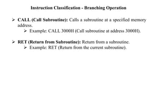
  • 35. Instruction Classification - Branching Operation ➢ CALL (Call Subroutine): Calls a subroutine at a specified memory address. ➢ Example: CALL 3000H (Call subroutine at address 3000H). ➢ RET (Return from Subroutine): Return from a subroutine. ➢ Example: RET (Return from the current subroutine).
  • 36. Instruction Classification - Machine Control Operations ➢ These instructions control the processor’s execution, such as halting the program (HLT) or enabling interrupts.