Design and minimization of reversible programmable logic arrays and its realization using pass transistors
Download as PPT, PDF1 like1,543 views

The document presents the design and minimization of reversible programmable logic arrays (RPLAs) using pass transistors, aiming to define a new architecture while reducing quantum costs and critical path delays. It discusses the principles of reversible computing and quantum computing, outlines the limitations of existing designs, and proposes an optimized architecture along with performance analyses. Key enhancements include reducing garbage outputs, optimizing gate usage, and improving throughput compared to existing designs.


![Reversible Computing
• Equal number of input states and output states
• Preserves an unique mapping between input and
output vectors for any Reversible circuit
• One or more operations can be united called
Reversible Gate
• (N x N) Reversible Gate has N number of inputs
and N number of outputs where N= {1, 2, 3, …}
[1] A. K. Biswas, M. M. Hasan, A. R. Chowdhury, and H. M. H. Babu, “Efficient approaches
for designing reversible binary coded decimalimplement in a single adders,”
Microelectronics Jounrnal, vol. 39, no. 12, pp. 1693–1703, December 2008.](https://image.slidesharecdn.com/designandminimizationofreversibleprogrammablelogicarraysanditsrealizationusingpasstransistors-131009065338-phpapp01/85/Design-and-minimization-of-reversible-programmable-logic-arrays-and-its-realization-using-pass-transistors-5-320.jpg)


![In Quantum Computing, encode information as a series of
quantum-mechanical states such as spin directions of electrons
or polarization orientations of a photon that might represent
as or might represent a superposition of the two values.
Encoded data is represented by qubits rather than bits
which can perform certain calculations exponentially
faster than conventional computing.
10 βα +=q
Quantum Computing
[2]W. N. N. Hung, X. Song, G. Yang, J. Yang, and M. Perkowski, “Quantum logic synthesis by
symbolic reachability analysis,” in 41st
Conference on (DAC’04), Design Automation
Conference, May 2004, pp. 838–841.](https://image.slidesharecdn.com/designandminimizationofreversibleprogrammablelogicarraysanditsrealizationusingpasstransistors-131009065338-phpapp01/85/Design-and-minimization-of-reversible-programmable-logic-arrays-and-its-realization-using-pass-transistors-8-320.jpg)


![Reversible Programmable Logic
Arrays
Reversible Programmable Logic Arrays was first proposed by A. R.
Chowdhury for multi-outputs function [4]. Reversible PLA
consists of following components:
1. Reversible AND Plane and 2. Reversible EX-OR Plane
Fig. 5: Reversible Programmable Logic Arrays](https://image.slidesharecdn.com/designandminimizationofreversibleprogrammablelogicarraysanditsrealizationusingpasstransistors-131009065338-phpapp01/85/Design-and-minimization-of-reversible-programmable-logic-arrays-and-its-realization-using-pass-transistors-12-320.jpg)
![Reversible Programmable Logic
Arrays…
The existing design [4] of Reversible Programmable Logic Arrays is
shown in Fig. 6.
Fig. 6: Existing design of Reversible PLAs.
[4] Ahsan Raja Chowdhury, Rumana Nazmul, Hafiz Md. Hasan Babu: A New Approach to
Synthesize Multiple-Output Functions Using Reversible Programmable Logic Array.
VLSI Design 2006: 311-316](https://image.slidesharecdn.com/designandminimizationofreversibleprogrammablelogicarraysanditsrealizationusingpasstransistors-131009065338-phpapp01/85/Design-and-minimization-of-reversible-programmable-logic-arrays-and-its-realization-using-pass-transistors-13-320.jpg)


Design and minimization of reversible programmable logic arrays and its realization using pass transistors
- 1. Design and Minimization of Reversible Programmable Logic Arrays and Its Realization using Pass Transistors Supervised by Dr. Hafiz Md. Hasan Babu Professor, Dept. of Computer Science and Engineering University of Dhaka, Dhaka-1000, Bangladesh E-mails: hafizbabu@hotmail.com Presented by Sajib Kumar Mitra MS Student, Dept. of Computer Science and Engineering University of Dhaka, Dhaka-1000, Bangladesh E-mails: sajibmitra.csedu@yahoo.com
- 2. Purposes • Define an new Architecture of RPLAs • Minimization of Quantum Cost • Reduction of Critical Path Delay • Reduction of Number of Gates • Garbage Outputs Optimization • Pass Transistor Realization of RPLAs
- 3. Overview • Reversible and Quantum Computing • Reversible Programmable Logic Arrays • Proposed Architecture of Reversible PLAs • Delay Calculation of Reversible PLAs • Pass Transistor Realization of MUX Gate • Performance Analysis • Conclusion
- 4. Reversible and Quantum Computing
- 5. Reversible Computing • Equal number of input states and output states • Preserves an unique mapping between input and output vectors for any Reversible circuit • One or more operations can be united called Reversible Gate • (N x N) Reversible Gate has N number of inputs and N number of outputs where N= {1, 2, 3, …} [1] A. K. Biswas, M. M. Hasan, A. R. Chowdhury, and H. M. H. Babu, “Efficient approaches for designing reversible binary coded decimalimplement in a single adders,” Microelectronics Jounrnal, vol. 39, no. 12, pp. 1693–1703, December 2008.
- 6. • Limitation • Feedback is strictly restricted • Fan-out must be one always Fig. 1: Basic difference between Irreversible and Reversible Circuits Reversible Computing…
- 7. Fig. 2: Popular Reversible gates Reversible Computing…
- 8. In Quantum Computing, encode information as a series of quantum-mechanical states such as spin directions of electrons or polarization orientations of a photon that might represent as or might represent a superposition of the two values. Encoded data is represented by qubits rather than bits which can perform certain calculations exponentially faster than conventional computing. 10 βα +=q Quantum Computing [2]W. N. N. Hung, X. Song, G. Yang, J. Yang, and M. Perkowski, “Quantum logic synthesis by symbolic reachability analysis,” in 41st Conference on (DAC’04), Design Automation Conference, May 2004, pp. 838–841.
- 9. Quantum Computation uses matrix multiplication rather than conventional Boolean operations and the information measurement is realized by calculation the state of qubits . The matrix operations over qubits are simply specifies by using quantum primitives. For example, Fig. 3: Reversible behavior of Quantum matrix operation Quantum Computing…
- 10. Input Output A B P Q 0 0 0 0 0 1 0 1 1 0 1 1 1 1 1 0 Input/output Pattern Symbol 00 a 01 b 10 c 11 d Quantum Computing… Fig. 4: Working Principle of Unitary Controlled NOT (UCN)
- 11. Reversible Programmable Logic Arrays
- 12. Reversible Programmable Logic Arrays Reversible Programmable Logic Arrays was first proposed by A. R. Chowdhury for multi-outputs function [4]. Reversible PLA consists of following components: 1. Reversible AND Plane and 2. Reversible EX-OR Plane Fig. 5: Reversible Programmable Logic Arrays
- 13. Reversible Programmable Logic Arrays… The existing design [4] of Reversible Programmable Logic Arrays is shown in Fig. 6. Fig. 6: Existing design of Reversible PLAs. [4] Ahsan Raja Chowdhury, Rumana Nazmul, Hafiz Md. Hasan Babu: A New Approach to Synthesize Multiple-Output Functions Using Reversible Programmable Logic Array. VLSI Design 2006: 311-316
- 14. Reversible Programmable Logic Arrays… Limitation of Previous Design: 1. Toffoli gate produces huge number of unused outputs which are same as primary inputs. 2. Used Conventional Architecture (Complement and non-complement lines for copying input variables) 3. Requires huge number of Gates
- 15. Proposed Architecture of Reversible PLAs
- 16. Proposed Architecture of Reversible PLAs Proposed Design of RPLAs composed of followings: 1. EX-OR plane Optimization by using FG 2. Construction of AND plane by using MUX and FG 3. Delay Calculation based on Greedy Approach We have used the following example to represent the Proposed Design of RPLAs.
- 17. Proposed Architecture of Reversible PLAs… Construction of EX-OR plane : 1. EX-OR plane is constructed based on the ordering of the size of Products of functions 2. EX-OR plane defines the particular order of all products which will be followed by AND plane Fig. 7: Optimized design of Reversible PLAs by using FG.
- 18. Proposed Architecture of Reversible PLAs…
- 19. Proposed Architecture of Reversible PLAs… Sorted list of functions is: f4 f2 f1 f3 f5 f1 f2 f3 f4 f5 ab’ X X X ab’c X X a’b’c X bc’ X X ac X X X Size of Function 2 2 3 1 3 Functions Products
- 20. Proposed Architecture of Reversible PLAs… f1 f2 f3 f4 f5 ab’ X X X ab’c X X a’b’c X bc’ X X ac X X X Optimization of EX-OR Plane according to sorted list of functions is: f4 f2 f1 f3 f5 f4 ac a’b’c f2 4 f1 4ab’ ab’c f3 4 4 bc’ 4 4 2 f5
- 21. Proposed Architecture of Reversible PLAs… Theorem 1: Minimum number of Feynman gates to realize EX-OR plane is: n + m – TDOT Where , n= number of EX-OR operations m= number of output functions TDOT= total number of cross-points f4 ac a’b’c f2 4 f1 4ab’ ab’c f3 4 4 bc’ 4 4 2 f5
- 22. Proposed Architecture of Reversible PLAs… Construction of AND plane : 1.AND plane is constructed based on the ordering of the Products 2. MUX and FG gates are used to design AND plane 3. Two different patterns of MUX gates have been used in proposed design as follows: Fig. 14: Reversible MUX gate and two different templates of MUX gate which are used in proposed design.
- 23. Proposed Architecture of Reversible PLAs…
- 24. Proposed Architecture of Reversible PLAs… Fig. 2: Proposed Architecture of Reversible PLAs. Fig. 8: Proposed design of Reversible Programmable Logic Arrays
- 25. Delay Calculation of Reversible PLAs
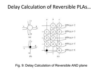
- 26. Delay Calculation of Reversible PLAs… We divide the calculation into two phases: a. AND Plane Delay and b. EX-OR Plane Delay Then we have merged both of the delay respect to both planes. In further realization of delay calculation, we consider the following things: a. Gate (Via) is represented as circle (DOT). b. Delay of any gate is 1 and via (DOT) denotes 0. c. Decimal value shows the delay of circle
- 27. Delay Calculation of Reversible PLAs…
- 28. Delay Calculation of AND Plane Delay Calculation of Reversible PLAs… Fig. 9: Delay Calculation of Reversible AND plane
- 29. Delay Calculation of AND Plane Delay Calculation of Reversible PLAs… Delay Calculation of Reversible AND plane ac a’b’c 5 ab’ ab’c 6 6 bc’ 2 2 2 1 6 5 6 a b c
- 30. Delay Calculation of AND Plane Delay Calculation of Reversible PLAs… Delay Calculation of Reversible AND plane for each Product line, APD (Pi) APD (P4)= 2 1 a b c Start 2 1 2 3 2 3 3 4 5 6 T L B R T L B R APD (P1)= 3 APD (P0)= 3 APD (P3)= 5 APD (P2)= 6
- 31. Delay Calculation of EX-OR Plane Delay Calculation of Reversible PLAs… Fig. 10: Delay Calculation of Reversible EX-OR plane
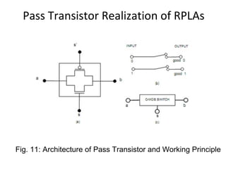
- 32. Pass Transistor Realization of RPLAs
- 33. Delay Calculation of EX-OR Plane Pass Transistor Realization of RPLAs Fig. 11: Architecture of Pass Transistor and Working Principle
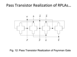
- 34. Delay Calculation of EX-OR Plane Pass Transistor Realization of RPLAs… Fig. 12: Pass Transistor Realization of Feynman Gate
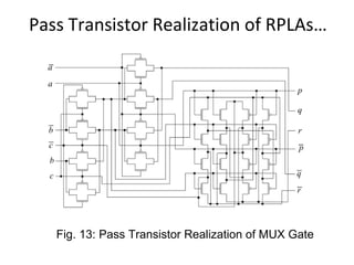
- 35. Delay Calculation of EX-OR Plane Pass Transistor Realization of RPLAs… Fig. 13: Pass Transistor Realization of MUX Gate
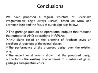
- 38. Conclusions We have proposed a regular structure of Reversible Programmable Logic Arrays (RPLAs) based on MUX and Feynman logic and the focus of our design is as follows: The garbage outputs as operational outputs that reduced the number of AND operations in RPLAs. AND plane based on the ordering of Products gives an excellent throughput of the overall design. The performance of the proposed design over the existing one. The experimental results show that the proposed design outperforms the existing one in terms of numbers of gates, garbages and quantum costs.
- 39. Thank you