Logic Design - Book: Final notes without combinational
7 likes1,943 views

The document provides a comprehensive overview of number systems and codes, focusing on binary, octal, and hexadecimal representations, as well as conversions between them. It also covers binary arithmetic operations, including addition, subtraction, multiplication, and division, along with examples and discussions of overflow conditions. Additionally, the document includes sections on logic gates, Boolean algebra, Karnaugh maps, sequential logic, and counters, demonstrating their applications in digital systems.


![CHAPTER 1
NUMBER SYSTEMS AND CODES
Example:
To Evaluate (5621)10 each digit is multiplied by the
weight of its position which is a power of 10.
5621 = 1x100 + 2x101 + 6x10² + 5x10³
A similar approach is followed in the other
numbering systems with a variation in the base (10, 2, 8,
16). In binary numbers, we can only use the digits 0 and
1 and the weights are powers of 2.
Table[I]
210
29
28
1024 512 256
27
128
26
64
25
32
24
16
23
8
22
4
21
2
20
1
Binary to Decimal Conversion
To convert a binary number into decimal, we
multiply each bit (binary digit) by the weight of its
position and sum up the results.
Example:
Convert the binary number (11011011)2 to decimal.
Answer:
-6–](https://image.slidesharecdn.com/finalnoteswithoutcombinational-140108084640-phpapp02/85/Logic-Design-Book-Final-notes-without-combinational-6-320.jpg)
![CHAPTER 1
NUMBER SYSTEMS AND CODES
(11011011)2 = 1x 20+ 1x 21+ 1x 23+ 1x 24+ 1x 26+ 1x27 = 1
+ 2 + 8 +16 + 64 + 128 = 219
Decimal to Binary Conversion
There are two ways to make this
conversion; the repeated division-by-2-method (which
you have studied before) and the sum of weights method
(which will be illustrated now).
Sum of weights method:
To find a binary number that is equivalent to a decimal
number, we can determine the set of binary weights whose
sum is equal to the decimal number. We can use table[I] to
determine the highest weight that is less than the number
and put 1 in its position then subtracting it from the
number and repeating the same process until finding all the
1s in the number then filling the positions in between with
0s.
Example:
Convert the following decimal numbers to binary form:
13, 100, 65, and 189. Put your answer as eight bit
numbers.
Answer:
13 =
128
0
64
0
32
0
-7–
16
0
8
1
4
1
2
0
1
1](https://image.slidesharecdn.com/finalnoteswithoutcombinational-140108084640-phpapp02/85/Logic-Design-Book-Final-notes-without-combinational-7-320.jpg)


![CHAPTER 1
NUMBER SYSTEMS AND CODES
ASCII control characters
Name
NUL
SOH
STX
ETX
EOT
ENQ
ACK
BEL
BS
HT
LF
VT
FF
CR
SO
SI
DLE
DC1
DC2
DC3
DC4
NAK
SYN
ETB
CAN
EM
SUB
ESC
FS
GS
RS
Decimal
0
1
2
3
4
5
6
7
8
9
10
11
12
13
14
15
16
17
18
19
20
21
22
23
24
25
26
. 27
28
29
30
Hex
00
01
02
03
04
05
06
07
08
09
OA
OB
OC
OD
OE
OF
10
11
12
13
14
15
16
17
18
19
1A
1B
1C
ID
1E
- 39 –
..Key,
CTRL@
CTRL A
CTRL B
CTRL C
CTRL D
CTRL E
CTRL F
CTRL G
CTRL H
CTRL I
CTRL J
CTRL K
CTRL L
CTRL M
CTRL N
CTRL O
CTRL P
CTRL Q
CTRL R
CTRL S
CTRL T
CTRL U
CTRL V
CTRL W
CTRL X
CTRL Y
CTRL Z
CTRL [
CTRL /
CTRL ]
CTRL^
Description
null character
start of header
start of text
end of text
end
of
transmission
enquire
acknowledge
bell
backspace
horizontal tab
line feed
vertical tab
form feed (new
page) return
carriage
shift out
shift in
data link escape
device control 1
device control 2
device control 3
device control 4
negative
acknowledge
synchronize
end
of
transmission
cancel
block medium
end of
substitute
escape
file separator
group separator
record separator](https://image.slidesharecdn.com/finalnoteswithoutcombinational-140108084640-phpapp02/85/Logic-Design-Book-Final-notes-without-combinational-39-320.jpg)


![CHAPTER3
BOOLEAN ALGEBRA
Evaluating Logic Circuit Outputs
Once the Boolean expression for a circuit output has been obtained, the
output logic level can be determined for any set of input levels.
This are two examples of the evaluating logic circuit output:
Let A=0, B=1, C=1, D=1
X
= A'BC (A+D)'
= 0'•1•1• (0+1)'
= 1 •1•1• (1)'
= 1 •1•1• 0
=0
Let A=0, B=0, C=1, D=1, E=1
X
= [D+ ((A+B)C)'] • E
= [1 + ((0+0)1 )'] • 1
= [1 + (0•1)'] • 1
= [1+ 0'] •1
= [1+ 1 ] • 1
=1
- 85 –](https://image.slidesharecdn.com/finalnoteswithoutcombinational-140108084640-phpapp02/85/Logic-Design-Book-Final-notes-without-combinational-85-320.jpg)


![CHAPTER3
BOOLEAN ALGEBRA
Multivariable Theorems
The theorems presented below involve more than one variable:
(9)
(10)
(11)
(12)
(13a)
)13b)
(13c)
(14)
(15)
(16)
(17)
x + y = y + x (commutative law)
x • y = y • x (commutative law)
x+ (y+z) = (x+y) +z = x+y+z (associative law)
x (yz) = (xy) z = xyz (associative law)
x (y+z) = xy + xz (distributive law)
x + yz = (x + y) (x + z) (distributive law)
(w+x)(y+z) = wy + xy + wz + xz
x + xy = x [proof see below]
x + x'y = x + y
(x +y)(x + z) = x +yz
x + xy = x (absorption)
Proof of (14)
x + xy
= x (1+y)
= x • 1 [using theorem (6)]
= x [using theorem (2)]
x + x’y
= ( x + x’) (x + y) [theorem 13b]
= 1 (x +y)
= (x + y)
Proof of (15)
Proof of (16)
- 89 –](https://image.slidesharecdn.com/finalnoteswithoutcombinational-140108084640-phpapp02/85/Logic-Design-Book-Final-notes-without-combinational-89-320.jpg)

![CHAPTER3
BOOLEAN ALGEBRA
DeMorgan's Theorem
DeMorgan's theorems are extremely useful in simplifying
expressions in which a product or sum of variables is inverted. The two
theorems are:
(18) (x+y)' = x' • y'
(19) (x•y)' = x' + y'
Theorem (18) says that when the OR sum of two variables is inverted,
this is the same as inverting each variable individually and then ANDing
these inverted variables.
Theorem (19) says that when the AND product of two variables is
inverted, this is the same as inverting each variable individually and then
ORing them.
Example
X
= [(A'+C) • (B+D')]'
= (A'+C)' + (B+D')'
= (AC') + (B'D)
= AC' + B'D
- 91 –](https://image.slidesharecdn.com/finalnoteswithoutcombinational-140108084640-phpapp02/85/Logic-Design-Book-Final-notes-without-combinational-91-320.jpg)


![CHAPTER3
i.
iii.
v.
BOOLEAN ALGEBRA
{[(AB)'C]'D}'
(A+B')C'+D'
A'+B'+C'+D'
ii.
iv.
vi.
(A'+B')C+D'
A'+(B'+C')D
A+B+C+D
11. Using Boolean algebra, simplify the following expressions
as much as possible:
i.
iii.
v.
(A + B')(A+C)
ii.
AB+ ABC +A
iv.
(A'+C)(A'+C')(A+B+C'D)
A'B+A'BC'+A'BCD+A'BC'D'E
ABC[AB+ C (BC+AC)]
12. Apply DeMorgan's theorems to each expression:
i.
AB(C D)
ii.
AB(CD EF)
iii.
(A B C D)(ABCD)
iv.
(A B)(C D) (E F)(G H)
13. Given the following Boolean function:
F = xy'z+x'y'z+w'xy+wx'y+wxy
i.
ii.
iii.
iv.
v.
Obtain the truth table of the function.
Draw the logic diagram using the original Boolean expression.
Simplify the function to a minimum number of literals using
Boolean algebra.
Obtain the truth table of the function from the simplified
expression and show that5 it is the same as the one in part (i).
Draw the logic diagram from the simplified expression and
compare the total number of gates with the diagram of part (ii).
14. Express the following functions in a sum of minterms and
a product of maxterms?
- 108 –](https://image.slidesharecdn.com/finalnoteswithoutcombinational-140108084640-phpapp02/85/Logic-Design-Book-Final-notes-without-combinational-108-320.jpg)


![CHAPTER 5
0
1
1
1
0
1
FLIP FLOPS
0
0
0
Table[1]
It is obvious that if any of the inputs of the NOR gate is high
(logic 1), the output is low (logic 0). So, we always start the
analysis with the logic 1 input.
i. If
S = 1, R = 0
(set condition).
S = 1 will make the output of the lower NOR gate Q = 0.
Q is fed back to the upper NOR gate. R = 0 and Q = 0 will
make the output of the upper NOR gate Q = 1.
Q is also fed back to the lower NOR. S = 1 and Q = 1 will
make the output of the lower NOR stable at 0 ( Q = 0 ).
Therefore, the circuit will latch in the set situation.
ii. if S = 0, R = 1
(Reset condition).
R = 1 will make the output of the upper NOR gate Q = 0.
Q is fed back to the lower NOR gate. S = 0 and Q = 0
will make the output of the lower NOR gate Q = 1.
Q is also fed back to the upper NOR gate. R=1 and Q
=1 will make the output of the upper NOR stable at 0 (Q
-125-](https://image.slidesharecdn.com/finalnoteswithoutcombinational-140108084640-phpapp02/85/Logic-Design-Book-Final-notes-without-combinational-125-320.jpg)


![CHAPTER 5
FLIP FLOPS
after the forbidden condition SR = 11 we will get
unpredictable result.
This is known as the race
situation.
If we go from SR = 11 to SR = 00, then we may have
two cases.
Case 1: R changes first: SR = 10 then SR = 00
Case 2: S changes first: SR = 01 then SR = 00
Case 1
S
R
Case 2
S
R
Q
Q
t1
0
11
0
t0
1
1
0
t2
1
10
1
t1
0
1
0
t3
2
00
1
t2
0
0
0
Table[2]
Table[3]
It is obvious that the output of the circuit depends on
which input reaches 0 first. That is why we call it the
race condition.
R
The function table of the NOR S-R latch is:
S
Q
Q
Comments
-128-](https://image.slidesharecdn.com/finalnoteswithoutcombinational-140108084640-phpapp02/85/Logic-Design-Book-Final-notes-without-combinational-128-320.jpg)
![CHAPTER 5
FLIP FLOPS
0
0
Q
Q
No change ( hold ) condition
0
1
1
0
Set.
1
0
0
1
reset
1
1
0
0
Forbidden, Not used , race.
Table[4]
Cross- NAND S-R latch . ( active low ).
An S-R latch can be made from cross – NAND gates ( Fig. 6 ). It
has similar function to the NOR latch, but the inputs are active low.
It is some times called S - R latch.
The truth table of NAND gate .
A
0
0
1
1
B
0
1
0
1
C
1
1
1
0
Table[5]
The key in analyzing this circuit is that if any of the
inputs at the NAND gate is 0, then the output is 1
regardless of the other input . So, we start the analysis
by active low (0) input.
The key in analyzing the previous circuit is that if
any of the inputs al the NAND gate is 0, then the
-129-](https://image.slidesharecdn.com/finalnoteswithoutcombinational-140108084640-phpapp02/85/Logic-Design-Book-Final-notes-without-combinational-129-320.jpg)

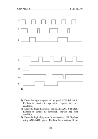
![CHAPTER 5
FLIP FLOPS
Table[6]
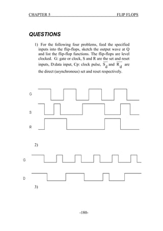
QUESTION:
If we put an inverter at both S and R inputs as shown in Fig (7),
analyze the resulting circuit and determine its function table.
-131-](https://image.slidesharecdn.com/finalnoteswithoutcombinational-140108084640-phpapp02/85/Logic-Design-Book-Final-notes-without-combinational-131-320.jpg)

![CHAPTER 5
FLIP FLOPS
Solution:
1-X = 0, Y = 0 (X is active low. Y is active high)
X=0→Q=1
Q = 1, Y = 0 → P = 0
2-X = 0, Y = 1
X=0→Q=1
Y=1→P=0
3-X = 1, Y = 1
Y=1→P=0
P = 0, X = 1 → Q = 1
4-X = 1, Y = 0
If: Q (t) = 1, Y = 0 → P (t+1) = 0
P (t+1) = 0, X = 1 → Q (t+1) = 1
This circuit can not work as a flip-flop because it has only one
stable state (P = 0 and Q = 1). Its function table Is shown in below:
X
0
0
1
1
Y
0
1
0
1
Q
1
1
1
1
P
0
0
0
0
Table[7]
-133-](https://image.slidesharecdn.com/finalnoteswithoutcombinational-140108084640-phpapp02/85/Logic-Design-Book-Final-notes-without-combinational-133-320.jpg)

![CHAPTER 5
FLIP FLOPS
Solution: See Fig (10).
R
0
0
1
1
S
0
1
0
1
Q(t+1)
*
0
1
Q(t)
forbidden
reset
set
No-change
Table [8]
The function table of the S-R NOR latch (active low) is shown in
the previous table. Initially Q = 0, and S = R = 1 (no change). At
time 1, S changes to 0 and R remains 1. The latch sets and Q = 1.
At time 2 S = 1 and R changes to 0 (reset) and Q changes to 0. At
time 3 both S and R become 1 (no change), and Q is still 1. This
applies to all the points as shown in figure (10).
So the latch sets at points where S changes from 1 to 0 and R = 1.
It resets at points where R changes from 1 to 0 and S = 1. At points
where S = R = 1, Q does not change.
-135-](https://image.slidesharecdn.com/finalnoteswithoutcombinational-140108084640-phpapp02/85/Logic-Design-Book-Final-notes-without-combinational-135-320.jpg)

![CHAPTER 5
1
1
0
1
FLIP FLOPS
0
*
reset
forbidden
Table[9]
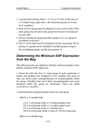
Switch Debouncing Circuits :
Switch bounce occurs as a mechanical switch lever
snaps to a new position. After reaching the new contact
point, the pole bounces on a micrometer scale of
millisecond duration (Fig (12)). Bounce can cause
problems in circuits that are expecting an input to
stabilize without oscillating, such as counters.
As shown in Fig (12), if you flip a mechanical SPDT
(single Pole double throw) switch to a new position, it will
bounce a few times before settling. We do not want a
counter circuit, for exople , to count these bounces.
The S – R debouncer circuit is shown in Fig (13).
When the switch is neither connected to the lower pin nor
to the upper pin, both S and R equal + 5v ( Logic 1 ) and
the latch is in the no change state .
-137-](https://image.slidesharecdn.com/finalnoteswithoutcombinational-140108084640-phpapp02/85/Logic-Design-Book-Final-notes-without-combinational-137-320.jpg)

![CHAPTER 5
FLIP FLOPS
Switch Condition
Impossible
Upper pin contacted
Lower pin contacted
Neither pin contacted
R
0
1
0
1
Table[10]
-140-
S
0
0
1
1
Q
Q
*
*
1
0
0
1
No change](https://image.slidesharecdn.com/finalnoteswithoutcombinational-140108084640-phpapp02/85/Logic-Design-Book-Final-notes-without-combinational-140-320.jpg)
![CHAPTER 5
FLIP FLOPS
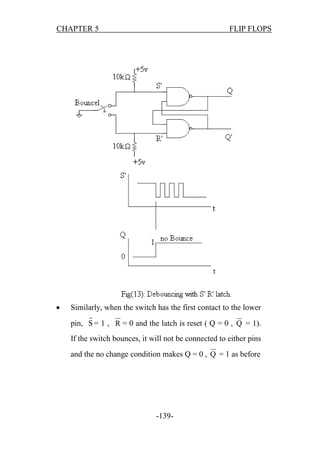
EXAMPLE 6:
Show how you can construct a switch debouncing circuit using a
NOR lath?
Solution:
As a single pole double throw (SPDT) switch makes a new contact,
it bounces a few times before settling. We do not want a count
circuit, for example, to count these bounces. A latch can be used to
eliminate this problem by forcing the lath to be in the no-change
condition when either pin is connected. The function table of the
latch, which is shown in fig (14), is shown in Table [XI].
Switch condition
Upper pin connected
Lower pin connected
Neither
pin
connected
Impossible
S
0
1
0
R
1
0
0
Q
0
1
No-change
1
1
*
Table[11]
In the timing diagram in Fig (14-b), at point A the switch is thrown
from position 1 to position 2. The output changes from logic 0 to
1. If the switch bounces around position 2, the latch will be in the
no-change condition and the output stays at logic 1. At point B in
the timing diagram, the switch is thrown from position 2 to position
1. The output changes from logic 1 to 0. If the switch bounces
around position 1, the latch will be in the no-change condition and
the output stays at logic 0. Therefore, the switch is debounced at
both positions.
-141-](https://image.slidesharecdn.com/finalnoteswithoutcombinational-140108084640-phpapp02/85/Logic-Design-Book-Final-notes-without-combinational-141-320.jpg)


![CHAPTER 5
FLIP FLOPS
The latch is only transparent when the gate is active (
gate =1) , otherwise it is in the hold state and the input (
S,R) has no effect on it .
The clocked (gated) latch can also be implemented
using cross – NAND gates as shown in fig (16) .
Try to analyze this circuit yourself. The function table of both
circuits is as follows.
Table[12]: Function table of gated flip – flop
S
R
Gate Q
Q Comments
X
X
0
Q The gate is open and
Q
the flip flop is in the
no change.
0
0
1
Q
Q No change
0
1
1
0
1
Reset
1
0
1
1
0
Set
-144-](https://image.slidesharecdn.com/finalnoteswithoutcombinational-140108084640-phpapp02/85/Logic-Design-Book-Final-notes-without-combinational-144-320.jpg)


![CHAPTER 5
FLIP FLOPS
Operating Mode
Inputs
Out puts
E
D
Q ( t +1)
Q (t +1 )
Data Enabled
1
0
0
1
Data Enabled
1
1
1
0
Data Latched
0
X
Q(t)
Q (t)
Table[13]
EXAMPLE 10:
Construct a D flip-flop using NOR and AND gates.
Solution:
J–K FLIP – FLOPS :
The J.K flip – flop ( Fig ( 23 a ) ) is similar to the S-R
flip – flop with Q fed back to be ANDed with R and Q
-149-](https://image.slidesharecdn.com/finalnoteswithoutcombinational-140108084640-phpapp02/85/Logic-Design-Book-Final-notes-without-combinational-149-320.jpg)


![CHAPTER 5
FLIP FLOPS
So, the next state will be the toggle (complement) of the present
state.
The function table of the J. K flip – flop is
J
K Gate Q(t+1 )
Q (t+1) Comments
X X 0
Q(t )
Q (t)
No-change ( gate is open)
0
0
1
Q(t )
Q (t)
No-change
0
1
1
0
1
Reset
1
0
1
1
0
Set
1
1
1
Q (t)
Q(t )
Toggle (complement)
Table[14]
T. (TOGGLE) FLIP–FLOP
Another type of flip- flop is the T- flip flop. It can be
obtained be connecting both J and K together. As shown in
figure ( 24 . )
-153-](https://image.slidesharecdn.com/finalnoteswithoutcombinational-140108084640-phpapp02/85/Logic-Design-Book-Final-notes-without-combinational-153-320.jpg)
![CHAPTER 5
FLIP FLOPS
The analysis of this circuit is very simple .
i-
If T = 0, then JK = 00 and the flip-flop is in the no-change
state
If T = 1, then JK = 11 and the flip – flop is in the toggle
ii-
state.
The function table of the flip-flop is :
T
Gate
Q(t+1 )
Q (t+1)
Comments
X
0
Q(t )
Q (t)
No-change ( gate is open)
0
1
Q(t )
Q (t)
No-change
1
1
Q (t)
Q(t )
Toggle (complement)
Table[15]
-154-](https://image.slidesharecdn.com/finalnoteswithoutcombinational-140108084640-phpapp02/85/Logic-Design-Book-Final-notes-without-combinational-154-320.jpg)


![CHAPTER 5
FLIP FLOPS
Solution:
Function table:
J
0
0
1
1
K
0
1
0
1
Clock
↓
↓
↓
↓
Q(t+1)
Q(t)
0
1
Q’(t+1)
function
No-change
reset
set
toggle
Table[16]
EXAMPLE 12:
Determine the Q output waveform if the inputs shown in Fig (30)
are applied to a clocked S-R flip flop that is initially RESET. The
flip-flop is triggered at the positive edge.
Solution: The clock and the S-R inputs are given and the
resulting Q output is shown. We take a line at each positive edge of
the clock and determine the value of S and R. So, Q can be set,
reset or no-change as shown.
-161-](https://image.slidesharecdn.com/finalnoteswithoutcombinational-140108084640-phpapp02/85/Logic-Design-Book-Final-notes-without-combinational-161-320.jpg)


![CHAPTER 5
FLIP FLOPS
Function table:
S
0
0
1
1
R
0
1
0
1
Clock
↓
↓
↓
↓
Q(t+1)
Q(t)
0
1
*
function
No-change
reset
set
forbidden
Table[17]
-165-](https://image.slidesharecdn.com/finalnoteswithoutcombinational-140108084640-phpapp02/85/Logic-Design-Book-Final-notes-without-combinational-165-320.jpg)

![CHAPTER 5
FLIP FLOPS
Function table:
T
0
1
Clock
↓
↓
Q(t+1)
Q(t)
Q’(t+1)
function
No-change
toggle
Table[18]
MASTER-SLAVE FLIP-FLOP AND 1S
CATCHING:
-167-](https://image.slidesharecdn.com/finalnoteswithoutcombinational-140108084640-phpapp02/85/Logic-Design-Book-Final-notes-without-combinational-167-320.jpg)
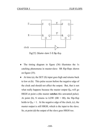


![CHAPTER 5
FLIP FLOPS
Table[19]
The direct inputs are active low, they must both be kept
HIGH for synchronous operation.
FIG (39) shows the logic diagram for an edge triggered J-K
flip-flop with active- low PRE and CLR inputs.
This figures illustrates basically how these inputs work.
They are connected so that they override the effect of the
synchronous inputs, ( J, K ) and the clock.
-173-](https://image.slidesharecdn.com/finalnoteswithoutcombinational-140108084640-phpapp02/85/Logic-Design-Book-Final-notes-without-combinational-173-320.jpg)


![CHAPTER 6
SEQUENTIAL CIRCUITS
CHAPTER 6
Sequential Circuit Analysis and
Design
FLIP-FLOP EXCITATION TABLES :
When it is required to analyze a sequential circuit, we are
given the flip-flop inputs and asked to give the
corresponding output.
To do that, we must know the characteristic table of the
give flip-flop. Table [20] shows the characteristic table of
the four types of flip-flops.
S
R
Q(t+1)
D
Q(t+1)
0
0
Q(t)
0
0
0
1
0
1
1
1
0
1
1
1
*
J
K
Q(t+1)
T
Q(t+1)
0
0
Q(t)
0
Q(t)
0
1
0
1
Q( t )
1
0
1
1
1
Q( t )
-185-](https://image.slidesharecdn.com/finalnoteswithoutcombinational-140108084640-phpapp02/85/Logic-Design-Book-Final-notes-without-combinational-185-320.jpg)
![CHAPTER 6
SEQUENTIAL CIRCUITS
Table [20] : Characteristic ( Function ) tables of the four types of
flip-flops.
* When it is required to design a sequential circuit the required
sequence of input-output of the circuit is given (present state – next
state of output), and it is required to design the input of the flip-flop
( S-R, T , J-K or D ) to give the desired output
e.g for an S-R sequential circuit:
analysis
(Q(t),Q (t+1))
S-R
design
* The excitation table is the reverse of the function ( characteristic)
table of the flip-flop. Table [21] shows the excitation table of S-R
flip-flop.
Present Next
state
0
Comments S
R Comments
0
0
No change
x
Q(t+1)
0
R
state
Q(t)
S
0
R is do not care because
both R = 0 and R = 1
0
1
give the required Q(t+1)
or reset
0
1
1
0
Set
1
0
1
0
0
1
Reset
0
1
1
1
0
0
No change x
0
S is
do not care
because both S = 0 and S
-186-](https://image.slidesharecdn.com/finalnoteswithoutcombinational-140108084640-phpapp02/85/Logic-Design-Book-Final-notes-without-combinational-186-320.jpg)
![CHAPTER 6
SEQUENTIAL CIRCUITS
1
0
= 1 give the required
or set
Q(t+1)
Table [21] : excitation table of SR flip – flop
* The excitation tables of all types of flip-flops are shown in table
[22]
Present Next
S
R
Present Next
D
state
state
state
state
Q(t)
Q(t+1)
Q(t)
Q(t+1)
0
0
0
x
0
0
0
0
1
1
0
0
1
1
1
0
0
1
1
0
0
1
1
x
0
1
1
1
J
K
Present Next
Present Next
T
state
state
state
state
Q(t)
Q(t+1)
Q(t)
Q(t+1)
0
0
0
x
0
0
0
0
1
1
x
0
1
1
1
0
x
1
1
0
1
1
1
X
0
1
1
0
Table [21] : Excitation table of the 4 – types of flip – flops.
-187-](https://image.slidesharecdn.com/finalnoteswithoutcombinational-140108084640-phpapp02/85/Logic-Design-Book-Final-notes-without-combinational-187-320.jpg)


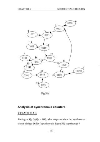


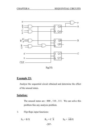

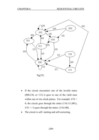

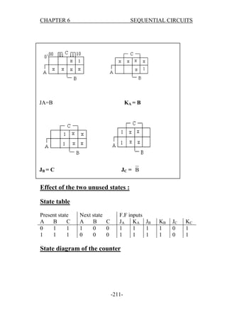


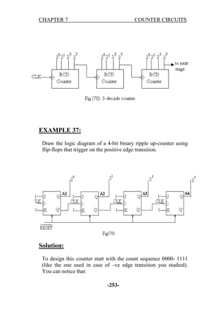
![CHAPTER 7
COUNTER CIRCUITS
If we have a 4 – bit binary counters, we would
count from 0000 up to 1111, which are 16 different
binary outputs.
We can determine the number of states (modulus)
of a binary counter by using the following formula:
Modulus = 2 N where N = number of flip – flips on the
condition that there are not any unused states.
Synchronous versus ripple counters:
[1]
If we look at a given clock pulse, e.g. pulse 7, the negative
edge C p causes Q0 to toggle low which causes Q1 to toggle
low which causes Q2 to toggle low. There will be a
propagation delay between the time that C p goes low until
Q2 finally goes low. Because of this delay, ripple counters
are called asynchronous counters, meaning that each flipflop is not triggered at exactly the same time. The
propagation delay – places limitations on the maximum
frequency allowed by the clock.
[2]
Synchronous counters can be formed by driving each flipflop’s clock by the same clock input. Synchronous counters
are more complicated than ripples counters.
DOWN COUNTERS:
-246-](https://image.slidesharecdn.com/finalnoteswithoutcombinational-140108084640-phpapp02/85/Logic-Design-Book-Final-notes-without-combinational-246-320.jpg)


Logic Design - Book: Final notes without combinational
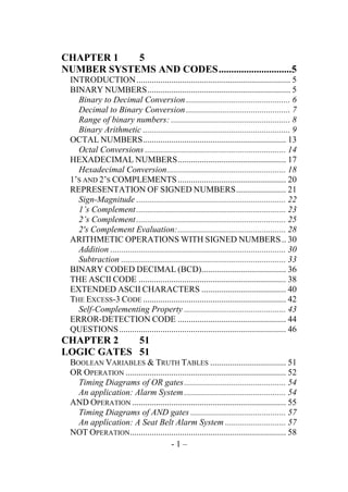
- 1. CHAPTER 1 5 NUMBER SYSTEMS AND CODES .............................5 INTRODUCTION ....................................................................... 5 BINARY NUMBERS .................................................................. 5 Binary to Decimal Conversion ................................................ 6 Decimal to Binary Conversion ................................................ 7 Range of binary numbers: ....................................................... 8 Binary Arithmetic .................................................................... 9 OCTAL NUMBERS .................................................................. 13 Octal Conversions ................................................................. 14 HEXADECIMAL NUMBERS .................................................. 17 Hexadecimal Conversion ....................................................... 18 1’S AND 2’S COMPLEMENTS .................................................. 20 REPRESENTATION OF SIGNED NUMBERS ....................... 21 Sign-Magnitude ..................................................................... 22 1’s Complement ..................................................................... 23 2’s Complement ..................................................................... 25 2's Complement Evaluation: .................................................. 28 ARITHMETIC OPERATIONS WITH SIGNED NUMBERS .. 30 Addition ................................................................................. 30 Subtraction ............................................................................ 33 BINARY CODED DECIMAL (BCD)....................................... 36 THE ASCII CODE .................................................................... 38 EXTENDED ASCII CHARACTERS ....................................... 40 THE EXCESS-3 CODE .................................................................. 42 Self-Complementing Property ............................................... 43 ERROR-DETECTION CODE .................................................. 44 QUESTIONS ............................................................................. 46 CHAPTER 2 51 LOGIC GATES 51 BOOLEAN VARIABLES & TRUTH TABLES ................................... 51 OR OPERATION .......................................................................... 52 Timing Diagrams of OR gates ............................................... 54 An application: Alarm System ............................................... 54 AND OPERATION ....................................................................... 55 Timing Diagrams of AND gates ............................................ 57 An application: A Seat Belt Alarm System ............................ 57 NOT OPERATION ........................................................................ 58 -1–
- 2. NOR OPERATION ....................................................................... 59 Negative AND equivalent of a NOR gate .............................. 60 An application: An aircraft landing indicator....................... 61 NAND OPERATION .................................................................... 62 Negative OR Equivalent Operation of the NAND Gate ........ 63 An application: An aircraft landing indicator....................... 64 THE EXCLUSIVE-OR AND EXCLUSIVE-NOR GATES...... 65 The Exclusive-OR Gate ......................................................... 65 The Exclusive-NOR Gate ....................................................... 66 Timing diagram ..................................................................... 67 INTEGRATED CIRCUIT LOGIC FAMILIES ......................... 67 Diode Logic (DL) .................................................................. 67 Resistor-Transistor Logic (RTL) ........................................... 69 Diode-Transistor Logic (DTL) .............................................. 70 Transistor-Transistor Logic (TTL) ........................................ 71 Emitter-Coupled Logic (ECL) ............................................... 73 CMOS Logic .......................................................................... 73 Fan-in .................................................................................... 77 Fan-out .................................................................................. 77 Comparison of performance characteristics of CMOS, TTL and ECL logic gates. ............................................................. 77 QUESTIONS ............................................................................. 78 CHAPTER 3 84 BOOLEAN ALGEBRA ............................................... 84 DESCRIBING LOGIC CIRCUITS ALGEBRAICALLY ......................... 84 EVALUATING LOGIC CIRCUIT OUTPUTS ..................................... 85 IMPLEMENTING CIRCUITS FROM BOOLEAN EXPRESSION ............ 87 BOOLEAN THEOREMS ................................................................. 88 DEMORGAN'S THEOREM ............................................................ 91 UNIVERSALITY OF NAND & NOR GATES ................................. 94 ALTERNATE LOGIC GATE REPRESENTATIONS ............................ 96 LOGIC SYMBOL INTERPRETATION............................................... 98 CANONICAL AND STANDARD FORMS ............................. 98 Minterms and Maxterms ........................................................ 99 Sum of Minterms .................................................................. 102 Product of Maxterms ........................................................... 103 STANDARD FORMS ........................................................... 104 QUESTIONS ............................................................................... 105 -2–
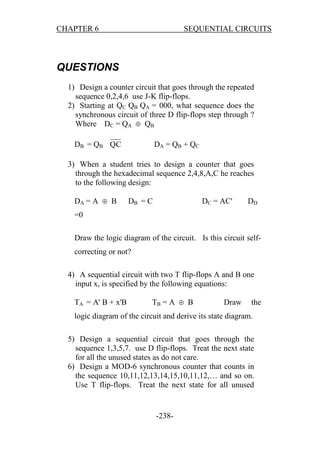
- 3. CHAPTER 4 110 THE KARNAUGH MAP .......................................... 110 THE THREE VARIABLE KARNAUGH MAP...................... 110 THE FOUR VARIABLE KARNAUGH MAP ........................ 111 KARNAUGH MAP SIMPLIFICATION OF SOP EXPRESSIONS ........ 111 DETERMINING THE MINIMUM SOP EXPRESSION FROM THE MAP ................................................................................................. 112 KARNAUGH MAP PRODUCT OF SUM (POS) SIMPLIFICATION ................................................................. 115 DON'T CARE CONDITIONS ................................................. 117 QUESTIONS: .......................................................................... 120 CHAPTER 5 122 SEQUENTIAL LOGIC AND FLIP-FLOPS ........... 122 INTRODUCTION ................................................................... 122 SEQUENTIAL CIRCUITS AND FEEDBACK: ..................... 122 Cross- NOR S-R latch ( active high ) .................................. 124 Cross- NAND S-R latch . ( active low ). .............................. 129 S – R Timing Analysis : ....................................................... 134 Switch Debouncing Circuits : .............................................. 137 STATE : ................................................................................... 142 CLOCKED SR LATCHES ( FLIP – FLOPS ) : .................................. 143 GATED D LATCH : ................................................................... 146 Integrated – circuit D latch ( 7475 ) : ................................. 147 J–K FLIP – FLOPS : ................................................................ 149 T. (TOGGLE) FLIP–FLOP ..................................................... 153 MASTER – SLAVE FLIP-FLOPS : ........................................ 155 EDGE – TRIGGERED J K FFS : ............................................. 159 MASTER-SLAVE FLIP-FLOP AND 1S CATCHING:.......... 167 DIRECT ( ASYNCHRONOUS ) INPUTS : ............................ 172 FLIP- FLOP OPERATING CHARACTERISTICS ................ 176 Propagation Delay times: .................................................... 176 SET-UP TIME ..................................................................... 178 HOLD TIME ........................................................................ 178 QUESTIONS ........................................................................... 180 CHAPTER 6 185 SEQUENTIAL CIRCUIT ANALYSIS AND DESIGN ....................................................... 185 -3–
- 4. FLIP-FLOP EXCITATION TABLES : ................................... 185 BASIC DEFINITIONS OF SEQUENTIAL CIRCUITS ......... 188 Sequential circuit : .............................................................. 188 State Versus Output: ............................................................ 188 Moore Circuits (Fig (46)) : ................................................. 188 Mealy Circuits: .................................................................... 189 COUNTERS ................................................................................ 190 STATE DIAGRAM: ..................................................................... 190 ANALYSIS OF A SEQUENTIAL CIRCUIT : ....................... 192 Analysis of synchronous counters........................................ 197 DESIGN OF SEQUENTIAL CIRCUITS : .............................. 200 Design with unused states : ................................................. 203 Design of counters : ............................................................. 210 QUESTIONS ........................................................................... 238 CHAPTER 7 242 COUNTER CIRCUITS ............................................. 242 CLASSIFICATION OF COUNTERS ..................................... 242 RIPPLE COUNTERS (ASYNCHRONOUS COUNTERS):... 243 3-bit Asynchronous Binary counter : (Mod-8) .................... 243 COUNT SEQUENCE .................................................................... 244 DOWN COUNTERS: .............................................................. 246 DESIGN OF DIVIDE – BY – N COUNTERS: ....................... 248 BCD RIPPLE (DECADE) COUNTER ................................... 251 SYNCHRONOUS COUNTERS: ............................................ 255 SYNCHRONOUS BINARY DOWN-COUNTER: ................ 258 UP/DOWN SYNCHRONOUS COUNTERS: ......................... 258 QUESTIONS ........................................................................... 260 CHAPTER 8 REGISTERS 263 263 REGISTER WITH PARALLEL LOAD : ................................ 263 SHIFT REGISTER BASICS: .................................................. 265 SERIAL IN/SERIAL OUT SHIFT REGISTERS: ................... 266 PARALLEL IN/SERIAL OUT SHIFT REGISTERS.............. 269 BIDIRECTIONAL SHIFT REGISTER: ................................. 273 RING SHIFT COUNTER AND JOHNSON SHIFT COUNTER: ................................................................................................. 277 Ring shift counter operation ................................................ 279 Johnson shift counter operation .......................................... 280 -4–
- 5. CHAPTER 1 NUMBER SYSTEMS AND CODES CHAPTER 1 NUMBER SYSTEMS AND CODES DIGITAL SYSTEM INTRODUCTION You have previously studied how to represent a number in decimal, binary, octal and hexadecimal numbering systems and also how to make a conversion from one representation to the other ones. In the following sections, we will make a quick overview of these skills. Then, we will illustrate how to represent negative numbers in binary and how to make arithmetic operations on them. After that a group of the most used codes and their common uses are given. Finally, two famous and simple error correction and detection codes are given. BINARY NUMBERS In the well known decimal numbering system, each position can represent 10 different digits from 0 to 9. each position has a weighting factor of powers of 10. -5–
- 6. CHAPTER 1 NUMBER SYSTEMS AND CODES Example: To Evaluate (5621)10 each digit is multiplied by the weight of its position which is a power of 10. 5621 = 1x100 + 2x101 + 6x10² + 5x10³ A similar approach is followed in the other numbering systems with a variation in the base (10, 2, 8, 16). In binary numbers, we can only use the digits 0 and 1 and the weights are powers of 2. Table[I] 210 29 28 1024 512 256 27 128 26 64 25 32 24 16 23 8 22 4 21 2 20 1 Binary to Decimal Conversion To convert a binary number into decimal, we multiply each bit (binary digit) by the weight of its position and sum up the results. Example: Convert the binary number (11011011)2 to decimal. Answer: -6–
- 7. CHAPTER 1 NUMBER SYSTEMS AND CODES (11011011)2 = 1x 20+ 1x 21+ 1x 23+ 1x 24+ 1x 26+ 1x27 = 1 + 2 + 8 +16 + 64 + 128 = 219 Decimal to Binary Conversion There are two ways to make this conversion; the repeated division-by-2-method (which you have studied before) and the sum of weights method (which will be illustrated now). Sum of weights method: To find a binary number that is equivalent to a decimal number, we can determine the set of binary weights whose sum is equal to the decimal number. We can use table[I] to determine the highest weight that is less than the number and put 1 in its position then subtracting it from the number and repeating the same process until finding all the 1s in the number then filling the positions in between with 0s. Example: Convert the following decimal numbers to binary form: 13, 100, 65, and 189. Put your answer as eight bit numbers. Answer: 13 = 128 0 64 0 32 0 -7– 16 0 8 1 4 1 2 0 1 1
- 8. CHAPTER 1 NUMBER SYSTEMS AND CODES 100 = 65 = 189 = 0 0 1 1 1 0 1 0 1 0 0 1 0 0 1 1 0 1 0 0 0 0 1 1 Range of binary numbers: We have used eight bit numbers for illustration because the 8-bit grouping is standard in most computers and has been given the special name byte. Using eight bits, 256 different numbers can be represented. Combining two bytes to get sixteen bits, 65,536 different numbers can be represented. Combining four bytes to get 32 bits, 4.295 X 10⁹ different numbers can be represented, and so on. The formula for finding the number of different combinations of n bits is Total combinations = 2n different numbers in the range 0 to (2n – 1) For example a 4-bit number can hold up to 2 =16 different values in the range 0 to 15 (0 to 1111). An 8-bit number can hold up to 28=256 different values in the range 0 to 255 (0 to 11111111). 4 Example: What is the range of values (in decimal) that can be represented by a binary number of the following number of bits: 10, 20 and 24. Solution: N=10 range = 0 to 210 – 1 = 0 to 1023 i.e. 1024 (1K)numbers -8–
- 9. CHAPTER 1 NUMBER SYSTEMS AND CODES N=20 range = 0 to 220 – 1 = 0 to 1048575 i.e. 1048576 (1M)numbers N=24 range = 0 to 224 – 1 = 0 to 16777215 i.e. 16777216 (16M)numbers Binary Arithmetic Binary Addition The four cases for adding binary digits (A + B) are as follows: A 0 0 1 1 B 0 1 0 1 S 0 1 1 0 C 0 0 0 1 Where: S is the sum and C is the carry. Example: Add the following binary numbers and put the result in 8-bits. Verify your answer by converting into decimal: a) 00111111 + 01111100 b) 11101101 + 01000011 Answer: a) 00111111 + 01111100 = 10111011 187) -9– (63 + 124 =
- 10. CHAPTER 1 NUMBER SYSTEMS AND CODES b) 11101101 + 01000011 = 100110000 This example shows that the result could not fit in 8-bits ( 237 + 67 = 304) and the maximum capacity of 8-bits is 255. That is what we call overflow. 1 0 0 1 1 0 1 0 1 1 1 1 1 1 1 1 1 1 1 1 1 1 1 0 0 1 0 1 1 1 1 1 1 1 0 0 1 0 0 1 0 0 1 1 1 1 0 0 1 1 0 0 1 0 1 1 1 0 0 Binary Subtraction The four cases for subtracting binary digits (A B) are as follows: A 0 0 1 1 B 0 1 0 1 D 0 1 1 0 B 0 1 0 0 Where: D is the difference and B is the borrow. Example: Subtract the following binary numbers and put the result in 8-bits. Verify your answer by converting into decimal: a) 10111111 - 01111100 b) 11101101 - 01000011 - 10 –
- 11. CHAPTER 1 NUMBER SYSTEMS AND CODES Answer: a) 10111111 - 01111100 = 01000011 (191 - 124 = 67) b) 11101101 - 01000011 = 10101010 (237 – 67 = 170) 0 1 0 0 10 0 1 1 1 1 1 1 1 1 1 1 1 0 0 1 0 0 0 0 1 1 0 10 1 1 1 0 1 1 0 1 0 1 0 0 0 0 1 1 1 0 1 0 1 0 1 0 Binary Multiplication The four cases for multiplying binary digits (A x B) are as follows: A 0 0 1 1 B 0 1 0 1 P 0 0 0 1 Where: P is the product. Example: Multiply the following binary numbers and put the result in 8-bits. Verify your answer by converting into decimal: a) 11100 x 101 b) 11011 x 1101 - 11 –
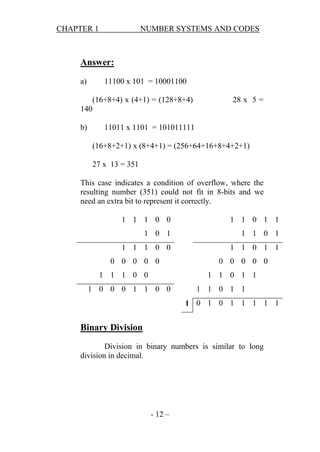
- 12. CHAPTER 1 NUMBER SYSTEMS AND CODES Answer: a) 11100 x 101 = 10001100 (16+8+4) x (4+1) = (128+8+4) 28 x 5 = 140 b) 11011 x 1101 = 101011111 (16+8+2+1) x (8+4+1) = (256+64+16+8+4+2+1) 27 x 13 = 351 This case indicates a condition of overflow, where the resulting number (351) could not fit in 8-bits and we need an extra bit to represent it correctly. 1 1 1 0 0 1 1 0 1 1 1 0 1 1 1 0 1 1 1 1 0 0 1 1 0 1 1 0 0 0 0 0 1 1 1 0 0 0 0 0 0 0 1 1 0 1 1 1 0 0 0 1 1 0 0 1 1 0 1 1 1 0 1 0 1 1 1 1 1 Binary Division Division in binary numbers is similar to long division in decimal. - 12 –
- 13. CHAPTER 1 NUMBER SYSTEMS AND CODES Example: Divide the following binary numbers and put the result in 8-bits. Verify your answer by converting into decimal: 11001 ÷ 101 Answer: a) 11001 ÷ 101 = 101 (16+8+1) ÷ (4+1) = (4+1) 25 ÷ 5 = 5 1 0 1 1 0 1 1 1 0 0 1 1 0 1 1 0 1 1 0 1 0 0 0 OCTAL NUMBERS The eight allowable digits are 0,1,2,3,4,5,6 and 7 and the weights are powers of 8. Decimal Binary Octal 0 1 2 0 1 2 000 001 010 - 13 –
- 14. CHAPTER 1 3 4 5 6 7 8 9 10 11 NUMBER SYSTEMS AND CODES 011 100 101 110 111 1000 1001 1010 1011 3 4 5 6 7 10 11 12 13 Octal Conversions Converting from binary to octal is simply a matter of grouping the binary positions in groups of three (starting at the least significant position) and writing down the octal equivalent. Example Convert the following binary numbers into octal: a) 10110111 b) 01101100 Solution: a) 10110111 = 010 101 111 = 257 (add a zero to the left and start from the least significant bit (LSB) make groups of three bits and convert each group into octal) b) 01101100 = 001 101 100 = 154 - 14 –
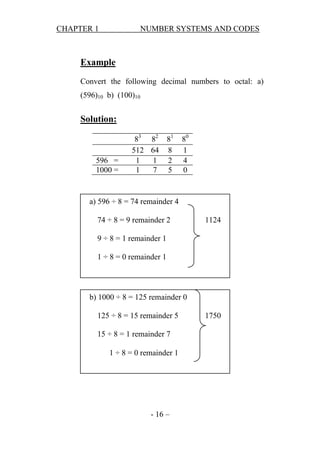
- 15. CHAPTER 1 NUMBER SYSTEMS AND CODES Example Convert the following octal number into binary: a) 327 b)601 Solution: a) 327 = 011 010 111 = 11010111 (replace each octal number with three equivalent binary numbers even if the number can be represented by less than three bits) b) 601 = 110 000 001 = 110000001 To convert from octal to decimal, (multiply by weighting factors). Example: Convert 713 to decimal. Solution: 713 = 7 x 82 + 1 x 81 + 3 x 80 = 459 To convert from decimal to octal, the successive-division procedure or the sum of weights procedure can be used. - 15 –
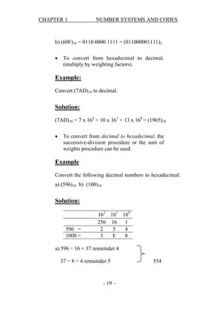
- 16. CHAPTER 1 NUMBER SYSTEMS AND CODES Example Convert the following decimal numbers to octal: a) (596)10 b) (100)10 Solution: 596 = 1000 = 83 82 81 512 64 8 1 1 2 1 7 5 80 1 4 0 a) 596 ÷ 8 = 74 remainder 4 74 ÷ 8 = 9 remainder 2 1124 9 ÷ 8 = 1 remainder 1 1 ÷ 8 = 0 remainder 1 b) 1000 ÷ 8 = 125 remainder 0 125 ÷ 8 = 15 remainder 5 15 ÷ 8 = 1 remainder 7 1 ÷ 8 = 0 remainder 1 - 16 – 1750
- 17. CHAPTER 1 NUMBER SYSTEMS AND CODES HEXADECIMAL NUMBERS The 16 allowable digits are 0,1,2,3,4,5,6,7,8,9,A,B,C,D,E and F and the weights are powers of 16. Decimal 0 1 2 3 4 5 6 7 8 9 10 11 12 13 14 15 16 17 18 19 20 Binary 0000 0000 0000 0001 0000 0010 0000 0011 0000 0100 0000 0101 0000 0110 0000 0111 0000 1000 0000 1001 0000 1010 0000 1011 0000 1100 0000 1101 0000 1110 0000 1111 0001 0000 0001 0001 0001 0010 0001 0011 0001 0100 Hexadecimal 00 01 02 03 04 05 06 07 08 09 0A 0B 0C 0D 0E 0F 10 11 12 13 14 - 17 –
- 18. CHAPTER 1 NUMBER SYSTEMS AND CODES Hexadecimal Conversion Converting from binary to hexadecimal is simply a matter of grouping the binary positions in groups of four (starting at the least significant position) and writing down the hexadecimal equivalent. Example Convert the following binary numbers into hexadecimal: a) 10101111 b) 01101100 Solution: a) 10110111 = 1011 0111 = (B 7)16 b) 01101100 = 0110 1100 = (6 C)16 Example Convert the following hexadecimal number into binary: a) A2E b)60F Solution: a) (A2E)16 = 1010 0010 1110 = (101000101110)2 (replace each hexadecimal number with four equivalent binary numbers even if the number can be represented by less than four bits) - 18 –
- 19. CHAPTER 1 NUMBER SYSTEMS AND CODES b) (60F)16 = 0110 0000 1111 = (011000001111)2 To convert from hexadecimal to decimal, (multiply by weighting factors). Example: Convert (7AD)16 to decimal. Solution: (7AD)16 = 7 x 162 + 10 x 161 + 13 x 160 = (1965)10 To convert from decimal to hexadecimal, the successive-division procedure or the sum of weights procedure can be used. Example Convert the following decimal numbers to hexadecimal: a) (596)10 b) (100)10 Solution: 596 = 1000 = 162 161 160 256 16 1 2 5 4 3 E 8 a) 596 ÷ 16 = 37 remainder 4 37 ÷ 8 = 4 remainder 5 - 19 – 554
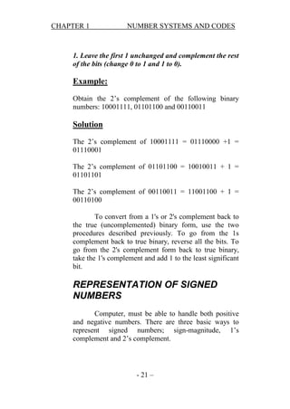
- 20. CHAPTER 1 NUMBER SYSTEMS AND CODES 5 ÷ 8 = 0 remainder 5 b) 1000 ÷ 16 = 62 remainder 8 62 ÷ 16 = 3 remainder 14 3E8 3 ÷ 16 = 0 remainder 3 1’s and 2’s COMPLEMENTS 1’s and 2’s complement allow the representation of negative numbers in binary. In most computers 2’s complement is used to represent negative numbers. The 1's complement of a binary number is found by simply changing all 1s to 0s and all 0s to 1s. Example: Obtain the 1’s complement of the following binary numbers: 10001111, 01101100 and 00110011 Solution The 1’s complement of 10001111 = 01110000 . The 1’s complement of 01101100 = 10010011 . The 1’s complement of 00110011 = 11001100 . The 2's complement of a binary number is found by adding 1 to the LSB of the 1 's complement. Another way of obtaining the 2’s complement of a binary number is to start with the LSB (the rightmost bit) and leave the bits unchanged until you find the first - 20 –
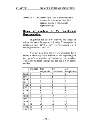
- 21. CHAPTER 1 NUMBER SYSTEMS AND CODES 1. Leave the first 1 unchanged and complement the rest of the bits (change 0 to 1 and 1 to 0). Example: Obtain the 2’s complement of the following binary numbers: 10001111, 01101100 and 00110011 Solution The 2’s complement of 10001111 = 01110000 +1 = 01110001 The 2’s complement of 01101100 = 10010011 + 1 = 01101101 The 2’s complement of 00110011 = 11001100 + 1 = 00110100 To convert from a 1's or 2's complement back to the true (uncomplemented) binary form, use the two procedures described previously. To go from the 1s complement back to true binary, reverse all the bits. To go from the 2's complement form back to true binary, take the 1's complement and add 1 to the least significant bit. REPRESENTATION OF SIGNED NUMBERS Computer, must be able to handle both positive and negative numbers. There are three basic ways to represent signed numbers; sign-magnitude, 1’s complement and 2’s complement. - 21 –
- 22. CHAPTER 1 NUMBER SYSTEMS AND CODES Sign-Magnitude The number consists of two parts: the MSB (most significant bit) represents the sign and the other bits represent the magnitude of the number. If the sign bit is 1 the number is negative and if it is 0 the number is positive. To illustrate this let us have an example. Example: Express each of the following numbers as an 8-bit number in sign-magnitude form: -30, 30, -121 and +99. Solution: -30 = 1 0011110 (The leftmost 1 indicates that the number is negative. The remaining 7bits carry the magnitude of 30) 30 = 0 0011110 (The only difference between –30 and +30 is the sign bit because the magnitude bits are similar in both numbers.) -121 = 1 1111001 99 = 0 1100011 - 22 –
- 23. CHAPTER 1 NUMBER SYSTEMS AND CODES Example: Find the decimal value of each of the following numbers if they are expressed in sign-magnitude form: 10111001 , 11111111 and 01111111. Solution: 10111001 = -57 (The leftmost 1 indicates that the number is negative. The remaining 7bits carry the magnitude of 57) 11111111 = -127 (The minimum number that can be represented in an 8-bit register using sign-magnitude representation) 01111111 = +127 (The maximum number that can be represented in an 8-bit register using sign-magnitude representation) Range of numbers in Sign-Magnitude Representation: In general for an n-bit number, the range of values that could be represented using sign-magnitude notation is from –(2n-1-1) to +(2n-1-1). For example if n=8 the range is from –127 to 127. 1’s Complement Negative numbers are represented in 1’s complement format whereas positive numbers are represented as the positive sign-magnitude numbers - 23 –
- 24. CHAPTER 1 NUMBER SYSTEMS AND CODES Example: Express each of the following numbers as an 8-bit number in 1’s complement form: 30, -30, -121 and +99. Solution: 30 = 00011110 -30 = 11100001 (the number equals the 1’s complement of 30) 121 = 01111001 -121 = 10000110 99 = 01100011 Example: Find the decimal value of each of the following numbers if they are expressed in 1’s complement form: 10111001 , 11111111 ,10000000 and 01111111. Solution: 10111001 = -01000110 = -70 (The leftmost 1 indicates that the number is negative. Take the 1’s complement of the number to get the magnitude of 70) - 24 –
- 25. CHAPTER 1 NUMBER SYSTEMS AND CODES 11111111 = -00000000 = -0 (That is one of the problem of 1’s complement representation, there are two representations of zero a positive one and a negative one.) 01111111 = +127 (The maximum number that can be represented in an 8-bit register using 1’s complement representation) 10000000 = -01111111 = -127 (The maximum number that can be represented in an 8-bit register using 1’s complement representation) Range of numbers Representation: in 1’s complement It is exactly the same as the range of numbers in sign-magnitude. 2’s Complement Negative numbers are represented in 2’s complement format whereas positive numbers are represented exactly the same way as in sign-magnitude and in 1’s complement. Example: Express each of the following numbers as an 8-bit number in 2’s complement form: 30, -30, -121 and +99. - 25 –
- 26. CHAPTER 1 NUMBER SYSTEMS AND CODES Solution: 30 = 00011110 -30 = 11100010 (the number equals the 2’s complement of 30) 121 = 01111001 -121 = 10000111 99 = 01100011 Example: Find the decimal value of each of the following numbers if they are expressed in 2’s complement form: 10111001 , 11111111 ,10000000 and 01111111. Solution: 10111001 = -01000111 = -71 (The leftmost 1 indicates that the number is negative. Take the 2’s complement of the number to get the magnitude of 71) 11111111 = -00000001 = -1 (The problem of two representations of zero is not found in 2’s complement.) 01111111 = +127 (The maximum number that can be represented in an 8-bit register using 2’s complement representation) - 26 –
- 27. CHAPTER 1 NUMBER SYSTEMS AND CODES 10000000 = -10000000 = -128 (The minimum number that can be represented in an 8-bit register using 2’s complement representation) Range of numbers Representation: in 2’s complement In general for an n-bit number, the range of values that could be represented using 2’s complement notation is from –(2n-1) to +(2n-1-1). For example if n=8 the range is from –128 to 127. You may note from the previous examples that a binary number may have different values depending on the type of representation used to interpret this number. The following table clarifies this fact for a 4-bit binary number. 0000 0001 0010 0011 0100 0101 0110 0111 1000 1001 1010 1011 1100 1101 unsigned Signmagnitude 0 0 1 1 2 2 3 3 4 4 5 5 6 6 7 7 8 -0 9 -1 10 -2 11 -3 12 -4 13 -5 - 27 – 1’s complement 0 1 2 3 4 5 6 7 -7 -6 -5 -4 -3 -2 2’s complement 0 1 2 3 4 5 6 7 -8 -7 -6 -5 -4 -3
- 28. CHAPTER 1 NUMBER SYSTEMS AND CODES 1110 14 1111 15 -6 -7 -1 -0 -2 -1 2's Complement Evaluation: Positive and negative numbers in the 2's complement system are evaluated by summing the weights in all bit positions where there are 1s and ignoring those positions where there are zeros. The weight of the sign bit in a negative number is given a negative value. EXAMPLE Determine the decimal values of the signed binary numbers expressed in 2's complement: (a) 01010110 (b) 10101010. Solution (a) The bits and their powers-of-two weights for the positive number are as follows: -27 26 25 24 23 22 21 2° 0 1 0 1 0 1 1 0 Summing the weights where there are 1's, - 28 –
- 29. CHAPTER 1 NUMBER SYSTEMS AND CODES 64 + 16 + 4 + 2 = +86 (b) The bits and their powers-of-two weights for the negative number are as follows. Notice that the negative sign bit has a weight of —27 = —128. -27 26 25 24 23 22 21 2° 1 0 1 0 1 0 1 0 Summing the weights where there are 1's, -128 + 32 + 8 + 2 = -86 From these examples, you can see one of the reasons why the 2's complement system is preferred for representing signed numbers: It simply requires a summation of weights regardless of whether the number is positive or negative. The sign-magnitude system requires two steps—sum the weights of the magnitude bits and examine the sign bit to determine if the number is positive or negative. The 1's complement system requires adding 1 to the summation of weights for negative numbers but not for positive numbers. - 29 –
- 30. CHAPTER 1 NUMBER SYSTEMS AND CODES Also, the 1's complement system is generally not used because two representations of zero (00000000 or 11111111) are possible. The 2's complement system is preferred and is used in most computers because it makes arithmetic operations easier, as you will see. ARITHMETIC OPERATIONS WITH SIGNED NUMBERS In the last section, you learned how signed numbers are represented in three different systems. In this section, you will learn how signed numbers are added and subtracted. Because the 2's complement system for representing signed numbers is the most widely used in computers and microprocessor-based systems, the coverage in this section is limited to 2 's complement arithmetic. The processes covered can be extended to the other systems if necessary. Addition The two numbers in an addition are the addend and the augend. The result is the sum. There are four cases that can occur when two signed binary numbers are added: 1. Both numbers positive 2. Positive number with magnitude larger than negative number - 30 –
- 31. CHAPTER 1 NUMBER SYSTEMS AND CODES 3. Negative number with magnitude larger than positive number 4. Both numbers negative Let's take one case at a time using 8-bit signed numbers as examples. The equivalent decimal numbers are shown for reference. Both numbers positive: 00000111 7 + 00000100 +4 00001011 11 The sum is positive and is therefore in true (uncomplemented) binary. Positive number with magnitude larger than negative number: 00001111 + 11111010 Discard carry —————1 15 + -6 00001001 9 The final carry bit is discarded. The sum is positive and therefore in true (uncomplented) binary. - 31 –
- 32. CHAPTER 1 NUMBER SYSTEMS AND CODES Negative number with magnitude larger than positive number: 00010000 + 11101000 11111000 16 + -24 -8 The sum is negative and therefore in 2's complement form. Discard carry—————> 11111011 —5 + 11110111 Both numbers negative: + -9 1 11110010 -14 The final carry bit is discarded. The sum is negative and therefore in 2's complement form.In a computer, the negative numbers are stored in 2's complement form so, as you can see, the addition process is very simple: Add the two numbers and discard any final carry bit. Overflow Condition When two numbers are added and the number of bits required to represent the sum exceeds the number of bits in the two numbers, an overflow results as indicated - 32 –
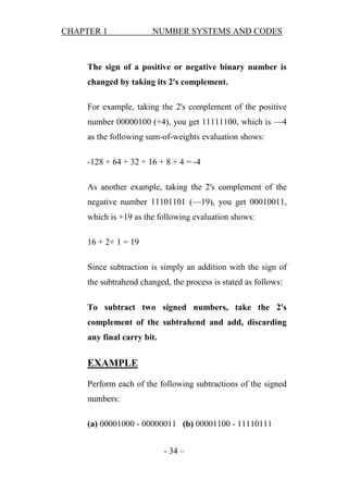
- 33. CHAPTER 1 NUMBER SYSTEMS AND CODES by an incorrect sign bit. An overflow can occur only when both numbers are positive or both numbers are negative. The following 8-bit example will illustrate this condition. 01111101 125 + 00111010 + 58 10110111 183 Sign incorrect Magnitude incorrect In this example the sum of 183 requires eight magnitude bits. Since there are seven magnitude bits in the numbers (one bit is the sign), there is a carry into the sign bit which produces the overflow indication. Numbers Are Added Two at a Time Subtraction Subtraction is a special case of addition. For example, subtracting +6 (the subtrahend from +9 (the minuend) is equivalent to adding —6 to +9. Basically, the subtraction operation changes the sign of the subtrahend and adds it to the minuend. The result of a subtraction is called the difference. - 33 –
- 34. CHAPTER 1 NUMBER SYSTEMS AND CODES The sign of a positive or negative binary number is changed by taking its 2's complement. For example, taking the 2's complement of the positive number 00000100 (+4), you get 11111100, which is —4 as the following sum-of-weights evaluation shows: -128 + 64 + 32 + 16 + 8 + 4 = -4 As another example, taking the 2's complement of the negative number 11101101 (—19), you get 00010011, which is +19 as the following evaluation shows: 16 + 2+ 1 = 19 Since subtraction is simply an addition with the sign of the subtrahend changed, the process is stated as follows: To subtract two signed numbers, take the 2's complement of the subtrahend and add, discarding any final carry bit. EXAMPLE Perform each of the following subtractions of the signed numbers: (a) 00001000 - 00000011 (b) 00001100 - 11110111 - 34 –
- 35. CHAPTER 1 NUMBER SYSTEMS AND CODES (c) 11100111 - 00010011 (d) 10001000 - 11100010 Solution Like in other examples, the equivalent decimal subtractions are given for reference. (a) In this case, 8 - 3 = 8 + (-3) = 5. 00001000 + 11111101 Minuend (+8) 2's complement of subtrahend (-3) Discard carry —> 1 00000101 Difference (+ 5) (b) In this case, 12 - (-9) = 12 + 9 = 21. 00001100 + 00001001 00010101 Minuend (+12) 2's complement of subtrahend (+9) Difference (+21) (c) In this case, -25 - (+19) = -25 + (-19) = -44. 11100111 Minuend (-25) - 35 –
- 36. CHAPTER 1 NUMBER SYSTEMS AND CODES + 11101101 2's complement of subtrahend (- 19) Discard carry —>1 11010100 Difference (-44) (d) In this case, -120 - (-30) = -120 + 30 = -90 10001000 + 00011110 Minuend (-120) 2's complement of subtrahend (+30) 10100110 Difference (-90) BINARY CODED DECIMAL (BCD) The binary coded decimal system is used to represent each of the ten decimal digits as a 4-bit binary code. This code is useful in dealing with decimal numbers. As you know a 4-bit binary number can represent up to 16 numbers (0-15) but there are only 10 decimal digits (0-9), so we have 6 representations (1015) which are not used in the BCD code. To convert a decimal number to BCD replace each digit with a corresponding 4-bit binary number even if the number can be represented by less than 4 bits. To convert a BCD number into decimal make groups of 4 bits starting from the LSB, if necessary add extra zeroes to the left then convert each 4-bits to decimal. Decimal 0 1 2 BCD 0000 0001 0010 - 36 –
- 37. CHAPTER 1 3 4 5 6 7 8 9 NUMBER SYSTEMS AND CODES 0011 0100 0101 0110 0111 1000 1001 Example: Convert the following decimal numbers to BCD: 125, 909 and 1476. Solution: (125)10 = 0001 0010 0101 (909)10 = 1001 0000 1001 (1476)10 = 0001 0100 0111 0110 Example: Convert the following BCD numbers to decimal: 100000101001, 1101110010, 110010000101. Solution: 1000 0010 1001 = (825)10 0011 0111 0010 = (372)10 - 37 – 1010000101 and
- 38. CHAPTER 1 NUMBER SYSTEMS AND CODES 0010 1000 0101= (285)10 1100 1000 0101 = This number can not be a BCD number because 1100 is the binary representation of 12 and this is not a valid decimal digit. THE ASCII CODE To get information into and out of a computer, we need more than just numeric representations; we also have to take care of all the letters and symbols used in day-to-day processing. Information such as names, addresses, and item descriptions must be input and output in a readable format. But remember that a digital system can deal only with 1's and 0's. Therefore, we need a special code to represent all alphanumeric data (letters, symbols, and numbers). Most industry has settled on an input/output (I/O) code called the American Standard Code for Information Interchange (ASCII). The ASCII code uses 7 bits to represent all the alphanumeric data used in computer I/O. Seven bits will yield 128 different code combinations, as listed in the following Table. Each time a key is depressed on an ASCII keyboard, that key is converted into its ASCII code and processed by the computer. Then, before outputting the computer contents to a display terminal or printer, all information is converted from ASCII into standard English. - 38 –
- 39. CHAPTER 1 NUMBER SYSTEMS AND CODES ASCII control characters Name NUL SOH STX ETX EOT ENQ ACK BEL BS HT LF VT FF CR SO SI DLE DC1 DC2 DC3 DC4 NAK SYN ETB CAN EM SUB ESC FS GS RS Decimal 0 1 2 3 4 5 6 7 8 9 10 11 12 13 14 15 16 17 18 19 20 21 22 23 24 25 26 . 27 28 29 30 Hex 00 01 02 03 04 05 06 07 08 09 OA OB OC OD OE OF 10 11 12 13 14 15 16 17 18 19 1A 1B 1C ID 1E - 39 – ..Key, CTRL@ CTRL A CTRL B CTRL C CTRL D CTRL E CTRL F CTRL G CTRL H CTRL I CTRL J CTRL K CTRL L CTRL M CTRL N CTRL O CTRL P CTRL Q CTRL R CTRL S CTRL T CTRL U CTRL V CTRL W CTRL X CTRL Y CTRL Z CTRL [ CTRL / CTRL ] CTRL^ Description null character start of header start of text end of text end of transmission enquire acknowledge bell backspace horizontal tab line feed vertical tab form feed (new page) return carriage shift out shift in data link escape device control 1 device control 2 device control 3 device control 4 negative acknowledge synchronize end of transmission cancel block medium end of substitute escape file separator group separator record separator
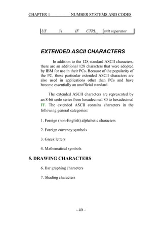
- 40. CHAPTER 1 US NUMBER SYSTEMS AND CODES 31 IF CTRL_ unit separator EXTENDED ASCII CHARACTERS In addition to the 128 standard ASCII characters, there are an additional 128 characters that were adopted by IBM for use in their PCs. Because of the popularity of the PC, these particular extended ASCII characters are also used in applications other than PCs and have become essentially an unofficial standard. The extended ASCII characters are represented by an 8-bit code series from hexadecimal 80 to hexadecimal FF. The extended ASCII contains characters in the following general categories: 1. Foreign (non-English) alphabetic characters 2. Foreign currency symbols 3. Greek letters 4. Mathematical symbols 5. DRAWING CHARACTERS 6. Bar graphing characters 7. Shading characters - 40 –
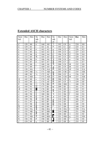
- 41. CHAPTER 1 NUMBER SYSTEMS AND CODES Extended ASCII characters Sym bol Dec Hex Ç ü é â ä à å ç ê ë è ï î ì Ä Å É æ Æ ô ö ò û ù ÿ Ö Ü ǿ £ ¥ P, ƒ 128 129 130 131 132 133 134 135 136 137 138 139 140 141 142 143 144 145 146 147 148 149 150 151 152 153 154 155 156 157 158 159 80 81 82 83 84 85 86 87 88 89 8A 8B 8C 8D 8E 8F 90 91 92 93 94 95 96 97 98 99 9A 9B 9C 9D 9E 9F Sy mb ol á í ó ú ñ Ñ ā ō ¿ ⌐ ¬ ½ ¼ ¡ « » ░ ▒ ▓ │ ┤ ╡ ╢ ╖ ╡ ╣ ║ ╗ ╝ ╜ ╛ ┐ Dee Hex 160 161 162 163 164 165 166 167 168 169 170 171 172 173 174 175 176 177 178 179 180 181 182 183 184 185 186 187 188 189 190 191 A0 Al A2 A3 A4 A5 A6 A7 A8 A9 AA AB AC AD AE AF B0 B1 B2 B3 B4 B5 B6 B7 B8 B9 BA BB BC BD BE BF Sy mb ol └ ┴ ┬ ├ ┤ ┼ ╞ ╟ ╚ ╔ ╩ ╦ ╠ ═ ╬ ╧ ╨ ╤ ╥ ╙ ╘ ╒ ╓ ╫ ╪ ┘ ┌ █ ▄ ▌ ▐ ▀ - 41 – Dec Hex Sym bol Dec Hex 192 193 194 195 196 197 198 199 200 201 202 203 204 205 206 207 208 209 210 211 212 213 214 215 216 217 218 219 220 221 222 223 C0 Cl C2 C3 C4 C5 C6 C7 C8 C9 CA CB CC CD CE CF DO Dl D2 D3 D4 D5 D6 D7 D8 D9 DA DB DC DD DE DF α β Γ π Σ б μ τ Φ Θ Ω δ ∞ Φ ε ∩ ≡ ± ≥ ≤ ∫ ÷ ≈ 224 225 226 227 228 229 230 231 232 233 234 235 236 237 238 239 240 241 242 243 244 245 246 247 248 249 250 251 252 253 254 255 E0 E1 E2 E3 E4 E5 E6 E7 E8 E9 EA EB EC ED EE EF F0 F1 F2 F3 F4 F5 F6 F7 F8 F9 FA FB FC FD FE FF ˚ • . √ η ² ▪
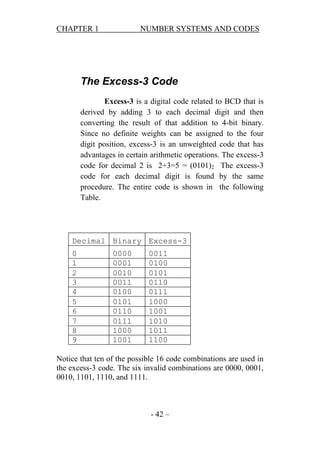
- 42. CHAPTER 1 NUMBER SYSTEMS AND CODES The Excess-3 Code Excess-3 is a digital code related to BCD that is derived by adding 3 to each decimal digit and then converting the result of that addition to 4-bit binary. Since no definite weights can be assigned to the four digit position, excess-3 is an unweighted code that has advantages in certain arithmetic operations. The excess-3 code for decimal 2 is 2+3=5 = (0101)2 The excess-3 code for each decimal digit is found by the same procedure. The entire code is shown in the following Table. Decimal Binary Excess-3 0 1 2 3 4 5 6 7 8 9 0000 0001 0010 0011 0100 0101 0110 0111 1000 1001 0011 0100 0101 0110 0111 1000 1001 1010 1011 1100 Notice that ten of the possible 16 code combinations are used in the excess-3 code. The six invalid combinations are 0000, 0001, 0010, 1101, 1110, and 1111. - 42 –
- 43. CHAPTER 1 NUMBER SYSTEMS AND CODES Example: Convert each of the following decimal numbers to excess-3 code: (A) 25 (B) 630 Solution First, add 3 to each digit in the decimal number, and then convert each resulting 4-bit sum to its equivalent binary code. (A) 25 = 01011000ADD THREE TO BOTH DIGITS TO BE 5 (0101) AND 8 (1000) THEN PUT THE REPRESENTATION OF ALL DIGITS TOGETHER. (b) 630 = 100101100011 as before 6 → 9 = (1001)2, 3 → 6 = (0110)2 and 0 → 3 = (0011)2. Self-Complementing Property The key feature of the excess-3 code is that it is selfcomplementing. This means that the 1's complement of an excess-3 number is the excess-3 code for the 9's complement of the corresponding decimal number. The 9's complement of a decimal number is found by subtracting each digit in the number from 9. For example, the 9's complement of 4 is 5. The excess-3 code for decimal 4 is 0111. The 1's complement of this is 1000, which is the excess-3 code for the decimal 5 (and 5 is the 9's complement of 4). - 43 –
- 44. CHAPTER 1 NUMBER SYSTEMS AND CODES The usefulness of the 9's complement and thus excess-3 stems from the fact that subtraction of a smaller decimal number from a larger one can be accomplished by adding the 9's complement (1's complement of the excess-3 code) of the subtrahend (in this case the smaller number) to the minuend and then adding the carry to the result. When subtracting a larger number from a smaller one, there is no carry, and the result is in 9's complement form and negative. This procedure has a distinct advantage over BCD in certain types of arithmetic logic. ERROR-DETECTION CODE Binary information can be transmitted from one location to another by electric wires or other communication medium. Any external noise introduced into the physical communication medium may change some of the bits from 0 to 1 or vice versa. The purpose of an error-detection code is to detect such bitreversal errors. One of the most common ways to achieve error detection is by means of a parity bit. A parity bit is an extra bit included with a message to make the total number of 1's transmitted either odd or even. A message of four bits and a parity bit P are shown in Table. If an odd parity is adopted, the P bit is chosen such that the total number of 1's is odd in the five bits that constitute the message and P. If an even parity is adopted, the P bit is chosen so that the total number of 1's in the five bits is even. Even parity being more common than odd parity. The parity bit is helpful in detecting errors during the transmission of information from one location to another. This is done in the following manner. An even parity bit is generated in the sending end for each message transmission. The message, together with the parity bit, is transmitted to its destination. The parity of the received data is checked. - 44 –
- 45. CHAPTER 1 NUMBER SYSTEMS AND CODES Parity bit Odd parity Message 0000 0001 0010 0011 0100 0101 0110 0111 1000 1001 1010 1011 1100 1101 1110 1111 P 1 0 0 1 0 1 1 0 0 1 1 0 1 0 0 Even parity Message 0000 0001 0010 0011 0100 0101 0110 0111 1000 1001 1010 1011 1100 1101 1110 P 0 1 1 0 1 0 0 1 1 0 0 1 0 1 1 1 1111 0 - 45 –
- 46. CHAPTER 1 NUMBER SYSTEMS AND CODES QUESTIONS 1) Convert the following unsigned binary numbers to decimal, octal, hexadecimal and BCD if possible. i. 10110010011 ii 110000111000 iii 1000111011 2) Convert the following decimal numbers to binary, octal, hexadecimal and BCD. i. 739 ii 504 iii 861 3) What is the minimum number of bits to represent each of the following unsigned decimal numbers: 5110, 256,451228 and 700. 4) Add, multiply, subtract (A-B) and divide (A/B) each of the following binary numbers: i. A = 11010011 B = 1101 ii. A = 101101 B= 101 iii. A = 11101001 B = 1101 5) Represent each of the following decimal numbers (when possible) as an 8-bit number in each of the following formats: sign-magnitude, 1’s complement and 2’s complement. i 134 328 ii -54 iii -128 iv –150 v 6) Represent each of the following decimal numbers (when possible) as a 16-bit number in each of the following formats: sign-magnitude, 1’s complement and 2’s complement. i 134 328 ii -54 iii -128 vi 1023 iv –150 7) For each of the following signed decimal numbers, what is the minimum number of bits to represent - 46 – v
- 47. CHAPTER 1 NUMBER SYSTEMS AND CODES each of them if you are using: sign-magnitude format, 1’s complement and 2’s complement formats. i 134 328 ii -54 iii -128 vi 1023 iv –150 8) Determine the decimal value of the following signed binary numbers if they are expressed in signmagnitude, 1’s complement and 2’s complement. i 10010011 ii 01011010 iv 11010001 iii 10000110 9) If A is a binary number, let COMP(A) be the 2’s complement of A. prove that COMP(COMP(A)) = A. 10) Show that overflow occurs in 2’s complement adddition when the carry-out of the left-most column is the complement of the carry-out of the column next to the left-most. Use four different examples to prove it. 11) An imaginary frog hops half the distance to its goal with eqach jump. Its first jump is 32cm. How far will it have gone after four jumps? Express your answer in binary and in decimal. 12) How many different values can be formed with an eight-bit code? How many different values can be formed if the most significant bit is always zero? 13) There are about 3000 characters in written Japanese. How many bits minimum would it take to represent the set of Japanese characters? 14) Perform the following arithmetic operations by changing the decimal numbers to 8-bit binary in 2’s complement representation. Check your answer by - 47 – v
- 48. CHAPTER 1 NUMBER SYSTEMS AND CODES changing the output from 2’s complement to decimal. 9 – 15, -28 – 64, -127 + 93, -50 + 100 15) Perform the following operations if the numbers are in 2’s complement representation. Check for your answer by transforming to decimal. Check if there is an overflow. i 10010101 – 11010110 ii 01101100 + 10111111 iii 10100011 + 11001100 iv 00111100 + 01010101 16) What is meant by the overflow? 17) Perform the following operations if the numbers are in 2’s complement representation. Indicate if there is an overflow or not. Check for your answer by transforming to decimal. i 01110101 + 01101010 ii 10010000 – 01000111 iii 11010011 – 10110000 iv 01100000 - 00111111 18) Perform the following operations if the numbers are in 2’s complement representation. Extend all the numbers to be represented in 8-bits before performing the operation. Indicate if there is an overflow or not. Check for your answer by transforming to decimal. i 1011 – 0110 ii iii 0110 – 0101010 iv 1001 – 110010 v 10101 + 0110 vi - 48 – 010111 – 1111 10111 + 0111
- 49. CHAPTER 1 NUMBER SYSTEMS AND CODES vii 1110 + 0101010 viii 11001 + 100010 19) Add an 8th bit for the following binary numbers to act once as an even parity and another time as an odd parity. i 1010001 ii 1111000 iii 1101110 iv 1110111 20) Convert the following decimal numbers to BCD and excess-3 . 102, 897, 954, 045, 621 and 378 21) Writ the following phrase by representing each alphanumeric in ASCII code. Use hex numbers for each character. “The Little Brown Fox Jumps Over The Dog...1,2,3,4,5,6,7,8,9” 22) What is the special property of excess-3 code that makes it suitable to represent decimal numbers. 23) Determine the signed decimal value of 10010010 for each of the following representations: abcd- Sign-magnitude representation. 2’s complement representation. BCD representation. Excess representation 24) Determine the signed decimal value of 01010110 for each of the following representations: a- Sign-magnitude representation. - 49 – Lazy
- 50. CHAPTER 1 bc- NUMBER SYSTEMS AND CODES 2’s complement representation. BCD representation. 25) -Perform the subtraction of (36 – 99)10 using the 2’s complement representation. Verify your answer by converting into decimal. - 50 –
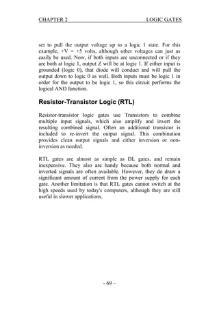
- 51. CHAPTER 2 LOGIC GATES CHAPTER 2 LOGIC GATES Boolean Variables & Truth Tables Boolean algebra differs in a major way from ordinary algebra in that boolean constants and variables are allowed to have only two possible values, 0 or 1. Boolean 0 and 1 do not represent actual numbers but instead represent the state of a voltage variable, or what is called its logic level. Some common representation of 0 and 1 is shown in the following diagram. LOGIC 0 False Off Low No Open Switch LOGIC 1 True On High Yes Close Switch In boolean algebra, there are three basic logic operations: OR, AND and NOT. These logic gates are digital circuits constructed from diodes, transistors, and resistors connected in such a way that the circuit output is the result of a basic logic operation (OR, AND, NOT) performed on the inputs. - 51 –
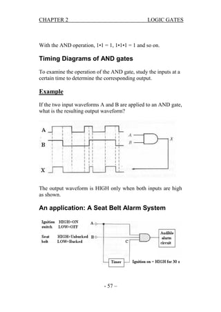
- 52. CHAPTER 2 LOGIC GATES Truth Table A truth table is a means for describing how a logic circuit's output depends on the logic levels present at the circuit's inputs. In the following two-inputs logic circuit, the table lists all possible combinations of logic levels present at inputs A and B along with the corresponding output level X. When either input A OR B is 1, the output X is 1. Therefore the function is an OR gate. OR Operation The expression X = A + B reads as "X equals A OR B". The + sign stands for the OR operation, not for ordinary addition. The OR operation produces a result of 1 when any of the input variable is 1. The OR operation produces a result of 0 only when all the input variables are 0. - 52 –
- 53. CHAPTER 2 LOGIC GATES An example of three input OR gate and its truth table is as follows: - 53 –
- 54. CHAPTER 2 LOGIC GATES With the OR operation, 1 + 1 = 1, 1+ 1 + 1 = 1 and so on. Timing Diagrams of OR gates A timing diagram is a graph that displays the relationship of two or more waveforms with respect to time. The following example explains the operation of an OR gate with pulsed inputs. Example If the two input waveforms A and B are applied to an OR gate, what is the resulting output waveform? An application: Alarm System A simplified portion of an intrusion detection and alarm system is shown. This system could be used for one room in a home a room with two windows and a door. The sensors are magnetic switches that produce a HIGH output when open and a LOW output when closed. As long as the windows and the door are secured, the switches are closed and all three of the OR gate inputs are LOW. When one of the windows or the door is opened, a HIGH is produced on that input to the OR gate and - 54 –
- 55. CHAPTER 2 LOGIC GATES the gate output goes HIGH. It then activates an alarm circuit to warn of the intrusion. AND Operation The expression X = A • B reads as "X equals A AND B". The multiplication sign stands for the AND operation, same for ordinary multiplication of 1s and 0s. The AND operation produces a result of 1 occurs only for the single case when all of the input variables are 1. The output is 0 for any case where one or more inputs are 0 - 55 –
- 56. CHAPTER 2 LOGIC GATES An example of three input AND gate and its truth table is as follows: - 56 –
- 57. CHAPTER 2 LOGIC GATES With the AND operation, 1•1 = 1, 1•1•1 = 1 and so on. Timing Diagrams of AND gates To examine the operation of the AND gate, study the inputs at a certain time to determine the corresponding output. Example If the two input waveforms A and B are applied to an AND gate, what is the resulting output waveform? The output waveform is HIGH only when both inputs are high as shown. An application: A Seat Belt Alarm System - 57 –
- 58. CHAPTER 2 LOGIC GATES an AND gate is used in a simple car seat belt alarm system to detect when the ignition switch is on and the seat belt is unbuckled. If the ignition switch is on, a HIGH is produced on input A of the AND gate. If the seat belt is not properly buckled, a HIGH is produced on input B of the AND gate. Also, when the ignition switch is turned on, a timer is started that produces a HIGH on input C for 30 s. If all three conditions exist—that is, if the ignition is on and the seat belt is unbuckled and the timer is running—the output of the AND gate is HIGH, and an audible alarm is energized to remind the driver. NOT Operation The NOT operation is unlike the OR and AND operations in that it can be performed on a single input variable. For example, if the variable A is subjected to the NOT operation, the result x can be expressed as x = A' where the prime (') represents the NOT operation. This expression is read as: x equals NOT A x equals the inverse of A x equals the complement of A Each of these is in common usage and all indicate that the logic value of x = A' is opposite to the logic value of A. The truth table of the NOT operation is as follows: - 58 –
- 59. CHAPTER 2 LOGIC GATES 1' = 0 because NOT 1 is 0 0' = 1 because NOT 0 is 1 The NOT operation is also referred to as inversion or complementation, and these terms are used interchangeably. NOR Operation NOR and NAND gates are used extensively in digital circuitry. These gates combine the basic operations AND, OR and NOT, which make it relatively easy to describe then using Boolean Algebra. NOR is the same as the OR gate symbol except that it has a small circle on the output. This small circle represents the inversion operation. Therefore the output expression of the two input NOR gate is: X = ( A + B )' - 59 –
- 60. CHAPTER 2 LOGIC GATES An example of three input OR gate can be constructed by a NOR gate plus a NOT gate: Negative AND equivalent of a NOR gate The truth table of the NOR gate shows that a HIGH is produced on the gate output only if all of the inputs are LOW. From this viewpoint, the NOR gate can be used for an AND operation that - 60 –
- 61. CHAPTER 2 LOGIC GATES requires all LOW inputs to produce a HIGH output. This mode of operation is called negative-AND. The term negative means that the inputs are defined to be in the active state when LOW. In the operation of a 2-input NOR gate functioning as a negative-AND gate, output X is HIGH if both inputs/A and B are LOW. An application: An aircraft landing indicator Problem: In an aircraft, as part of its functional monitoring system, a circuit is required to indicate the status of the landing gear prior to landing. A green LED display turns on if all three gears are properly extended when the "gear down" switch has been activated in preparation for landing. A red LED display turns on if any of the gears fail to extend properly prior to landing. When a landing gear is extended, its sensor produces a LOW voltage. When a landing gear is retracted, its sensor produces a HIGH voltage. Implement a circuit to meet this requirement. Solution Power is applied to the circuit only when the "gear down" switch is activated. Use a NOR gate for each of the two requirements as shown in figure. One NOR gate operates as a negative-AND to detect a LOW from each of the three landing geal sensors. When all three of the gate inputs are LOW, the - 61 –
- 62. CHAPTER 2 LOGIC GATES three landing gear are properly extended and the resulting HIGH output from the negative-AND gate turns on the green LED display. The other NOR gate operates as a NOR to detect if one or more of the landing gear remain retracted when the "gear down" switch is activated. When one or more of the landing gear remain retracted, the resulting HIGH from the sensor is detected by the NOR gate, which produces a LOW output to turn on the red LED warning display. NAND Operation NAND is the same as the AND gate symbol except that it has a small circle on the output. This small circle represents the inversion operation. Therefore the output expression of the two input NAND gate is: - 62 –
- 63. CHAPTER 2 LOGIC GATES X = ( AB )' Negative OR Equivalent Operation of the NAND Gate In the NAND gate's operation, one or more LOW inputs produce a HIGH output. The previous truth table shows that output X is HIGH (1) when any of the inputs, A and B, are LOW (0). From this viewpoint, the NAND gate can be used for an OR operation that requires one or more LOW inputs to produce a HIGH output. This mode of operation is referred to as negative-OR. The term negative means that the inputs are defined to be in the active state when LOW. - 63 –
- 64. CHAPTER 2 LOGIC GATES In the operation of a 2-input NAND gate functioning as a negative-OR gate, output X is HIGH if either input A or input B is LOW, or if both A and Bare LOW. An application: A Manufacturing Plant Tank Indicator Problem: A manufacturing plant uses two tanks to store a certain liquid chemical that is required in a manufacturing process. Each tank has a sensor that detects when the chemical level drops to 25% of full. The sensors produce a 5 V level when the tanks are more than one-quarter full. When the volume of chemical in a tank drops to one-quarter full, the sensor puts out a 0 V level. It is required that a single green light-emitting diode (LED) on an indicator panel show when both tanks are more than one quarter full. Show how a NAND gate can be used to implement this function. Solution: As long as both sensor outputs are HIGH, indicating that both tanks are more than one quarter full, the NAND gate output is LOW. The green LED circuit is arranged so that a low voltage turns it ON. - 64 –
- 65. CHAPTER 2 LOGIC GATES THE EXCLUSIVE-OR AND EXCLUSIVENOR GATES The exclusive-OR and exclusive-NOR gates are formed by the combination of other logic gates you have already studied. Because of their versatile range of applications, they are treated as basic gates and given their own symbols. The Exclusive- OR Gate The symbol of exclusive-OR (XOR for short) is shown along with its truth table. Inputs A 0 0 1 1 - 65 – output B 0 1 0 1 X 0 1 1 0
- 66. CHAPTER 2 LOGIC GATES The symbol used to express the XOR is: X = AB. From the truth table, the operation of the XOR can be summarized as: In an XOR gate operation, output X is HIGH if input A is LOW and input B is HIGH, or if input A is HIGH and input B is LOW; X is LOW if A and B are both HIGH or both LOW. The Exclusive-NOR Gate The symbol of exclusive-NOR (XNOR for short or equivalence) is shown along with its truth table. Inputs A 0 0 1 1 output B 0 1 0 1 X 1 0 0 1 The symbol used to express the XNOR is: X = AB. From the truth table, the operation of the XNOR can be summarized as: In an XNOR gate operation, output X is LOW if input A is LOW and input B is HIGH, or if input A is HIGH and input B is LOW; X is HIGH if A and B are both HIGH or both LOW. It is obvious that the XNOR is the complement of the XOR which is the reason of the bubble in the symbol of the XNOR. - 66 –
- 67. CHAPTER 2 LOGIC GATES Timing diagram EXAMPLE: INTEGRATED CIRCUIT LOGIC FAMILIES There are several different families of logic gates. Each family has its capabilities and limitations, its advantages and disadvantages. The following list describes the main logic families and their characteristics. You can follow the links to see the circuit construction of gates of each family. Diode Logic (DL) Diode logic gates use diodes to perform AND and OR logic functions. Diodes have the property of easily passing an electrical current in one direction, but not the other. Thus, diodes can act as a logical switch. Diode logic gates are very simple and inexpensive, and can be used effectively in specific situations. However, they cannot be used extensively, as they tend to degrade digital signals rapidly. - 67 –
- 68. CHAPTER 2 LOGIC GATES In addition, they cannot perform a NOT function, so their usefulness is quite limited. In the figure above, you see a basic Diode Logic OR gate. We'll assume that a logic 1 is represented by +5 volts, and a logic 0 is represented by ground, or zero volts. In this figure, if both inputs are left unconnected or are both at logic 0, output Z will also be held at zero volts by the resistor, and will thus be a logic 0 as well. However, if either input is raised to +5 volts, its diode will become forward biased and will therefore conduct. This in turn will force the output up to logic 1. If both inputs are logic 1, the output will still be logic 1. Hence, this gate correctly performs a logical OR function. The figure above shows the equivalent AND gate. We use the same logic levels, but the diodes are reversed and the resistor is - 68 –
- 69. CHAPTER 2 LOGIC GATES set to pull the output voltage up to a logic 1 state. For this example, +V = +5 volts, although other voltages can just as easily be used. Now, if both inputs are unconnected or if they are both at logic 1, output Z will be at logic 1. If either input is grounded (logic 0), that diode will conduct and will pull the output down to logic 0 as well. Both inputs must be logic 1 in order for the output to be logic 1, so this circuit performs the logical AND function. Resistor-Transistor Logic (RTL) Resistor-transistor logic gates use Transistors to combine multiple input signals, which also amplify and invert the resulting combined signal. Often an additional transistor is included to re-invert the output signal. This combination provides clean output signals and either inversion or noninversion as needed. RTL gates are almost as simple as DL gates, and remain inexpensive. They also are handy because both normal and inverted signals are often available. However, they do draw a significant amount of current from the power supply for each gate. Another limitation is that RTL gates cannot switch at the high speeds used by today's computers, although they are still useful in slower applications. - 69 –
- 70. CHAPTER 2 LOGIC GATES In this circuit, each transistor has its own separate input resistor, so each is controlled by a different input signal. However, the only way the output can be pulled down to logic 0 is if both transistors are turned on by logic 1 inputs. If either input is a logic 0 that transistor cannot conduct, so there is no current through either one. The output is then a logic 1. This is the behavior of a NAND gate. Of course, an inverter can also be included to provide an AND output at the same time. Diode-Transistor Logic (DTL) By letting diodes perform the logical AND or OR function and then amplifying the result with a transistor, we can avoid some of the limitations of RTL. DTL takes diode logic gates and adds a transistor to the output, in order to provide logic inversion and to restore the signal to full logic levels. - 70 –
- 71. CHAPTER 2 LOGIC GATES The above gate t is a DL OR gate followed by an inverter. The OR function is still performed by the diodes. However, regardless of the number of logic 1 inputs, there is certain to be a high enough input voltage to drive the transistor into saturation. Only if all inputs are logic 0 will the transistor be held off. Thus, this circuit performs a NOR function. The advantage of this circuit over its RTL equivalent is that the OR logic is performed by the diodes, not by resistors. Therefore there is no interaction between different inputs, and any number of diodes may be used. A disadvantage of this circuit is the input resistor to the transistor. Its presence tends to slow the circuit down, thus limiting the speed at which the transistor is able to switch states. Transistor-Transistor Logic (TTL) The physical construction of integrated circuits made it more effective to replace all the input diodes in a DTL gate with a transistor, built with multiple emitters. The result is transistor- - 71 –
- 72. CHAPTER 2 LOGIC GATES transistor logic, which became the standard logic circuit in most applications for a number of years. As the state of the art improved, TTL integrated circuits were adapted slightly to handle a wider range of requirements, but their basic functions remained the same. These devices comprise the 7400 family of digital ICs. The preceding figure shows an inverter designed with TTL logic. - 72 –
- 73. CHAPTER 2 LOGIC GATES The preceding figure shows a 4-input NAND gate designed with TTL logic. Emitter-Coupled Logic (ECL) Also known as Current Mode Logic (CML), ECL gates are specifically designed to operate at extremely high speeds, by avoiding the "lag" inherent when transistors are allowed to become saturated. Because of this, however, these gates demand substantial amounts of electrical current to operate correctly. CMOS Logic One factor is common to all of the logic families we have listed above: they use significant amounts of electrical power. Many applications, especially portable, battery-powered ones, require - 73 –
- 74. CHAPTER 2 LOGIC GATES that the use of power be absolutely minimized. To accomplish this, the CMOS (Complementary Metal-Oxide-Semiconductor) logic family was developed. This family uses enhancementmode MOSFETs as its transistors, and is so designed that it requires almost no current to operate. CMOS gates are, however, severely limited in their speed of operation. Nevertheless, they are highly useful and effective in a wide range of battery-powered applications. CMOS logic is a newer technology, based on the use of complementary MOS transistors to perform logic functions with almost no current required. This makes these gates very useful in battery-powered applications. The fact that they will work with supply voltages as low as 3 volts and as high as 15 volts is also very helpful. CMOS gates are all based on the fundamental inverter circuit shown above. Note that both transistors are enhancement-mode MOSFETs; one N-channel with its source grounded, and one Pchannel with its source connected to +V. Their gates are connected together to form the input, and their drains are connected together to form the output. The two MOSFETs are designed to have matching characteristics. Thus, they are complementary to each other. - 74 –
- 75. CHAPTER 2 LOGIC GATES When off, their resistance is effectively infinite; when on, their channel resistance is about 200 . Since the gate is essentially an open circuit it draws no current, and the output voltage will be equal to either ground or to the power supply voltage, depending on which transistor is conducting. When input A is grounded (logic 0), the N-channel MOSFET is unbiased, and therefore has no channel enhanced within itself. It is an open circuit, and therefore leaves the output line disconnected from ground. At the same time, the P-channel MOSFET is forward biased, so it has a channel enhanced within itself. This channel has a resistance of about 200 , connecting the output line to the +V supply. This pulls the output up to +V (logic 1). When input A is at +V (logic 1), the P-channel MOSFET is off and the N-channel MOSFET is on, thus pulling the output down to ground (logic 0). Thus, this circuit correctly performs logic inversion, and at the same time provides active pull-up and pulldown, according to the output state. - 75 –
- 76. CHAPTER 2 LOGIC GATES This concept can be expanded into NOR and NAND structures by combining inverters in a partially series, partially parallel structure Most logic families share a common characteristic: their inputs require a certain amount of current in order to operate correctly. CMOS gates work a bit differently, but still represent a capacitance that must be charged or discharged when the input changes state. The current required to drive any input must come from the output supplying the logic signal. Therefore, we need to know how much current an input requires, and how much current an output can reliably supply, in order to determine how many inputs may be connected to a single output. However, making such calculations can be tedious, and can bog down logic circuit design. Therefore, we use a different technique. Rather than working constantly with actual currents, we determine the amount of current required to drive one standard input, and designate that as a standard load on any output. Now we can define the number of standard loads a given output can drive, and identify it that way. Unfortunately, some - 76 –
- 77. CHAPTER 2 LOGIC GATES inputs for specialized circuits require more than the usual input current, and some gates, known as buffers, are deliberately designed to be able to drive more inputs than usual. For an easy way to define input current requirements and output drive capabilities, we define two new terms: Fan-in The number of standard loads drawn by an input to ensure reliable operation. Most inputs have a fan-in of 1. Fan-out The number of standard loads that can be reliably driven by an output, without causing the output voltage to shift out of its legal range of values. Comparison of performance characteristics of CMOS, TTL and ECL logic gates. Technology Device series Power dissipation: Static CMOS (silicon gate) 74HC At 100 kHz CMOS TTL TTL TTL TTL TTL ECL (metal std LS S ALS AS gate) 4000B 74 74LS 74S 74ALS 74AS 10KH 1 uW 10 mW 10 mW 10 ns 10 2 mW 2 mW 10 ns 19 mW 19 mW 3 ns 1 mW 20 20 20 0.17 mW Propagation 8 ns delay time Fan-out 0.1 mW 50 ns Std : standard LS: Low power Schottky - 77 – 1 mW 4 ns 8.5 mW 8.5 mW 1.5 ns 40 S: Schottky 25 mW 25 mW 1 ns
- 78. CHAPTER 2 LOGIC GATES ALS: Advanced Low power Schottky AS: Advanced Schottky QUESTIONS Choose the correct answers in the following questions. 1. Boolean algebra is different from ordinary algebra in which way? i. Boolean algebra can represent more than 1 discrete level between 0 and 1 ii. Boolean algebra have only 2 discrete levels: 0 and 1 iii. Boolean algebra can describe up to 3 levels of logic levels iv. They are actually the same v. NA The following 2 questions are referred to the below image: 2. What is the output X if both inputs A and B are 0? i. ii. iii. iv. 0 1 I don’t know NA 3. What is the output X if A=1 and B=0? - 78 –
- 79. CHAPTER 2 i. ii. iii. iv. LOGIC GATES 0 1 I don’t know NA 4. For a three inputs (A,B C) OR gate, what inputs are needed if output=0? i. ii. iii. iv. v. A=0, B=0, C=1 A=0, B=1, C=0 A=1, B=1, C=1 A=0, B=0,C=0 NA The following 2 questions are referred to the below image: 5. What is the output X if input A=1, B=0 and C=1? i. ii. iii. iv. 0 1 I don’t know NA 6. What inputs are needed if output=1? i. ii. iii. iv. v. A=0, B=0, C=0 A=1, B=0, C=1 A=0, B=1, C=0 A=1, B=1,C=1 NA - 79 –
- 80. CHAPTER 2 LOGIC GATES The following 2 questions are related to the below image: 7. What is the ouput of the above gate if input A=0, B=1? v. vi. vii. viii. 0 1 not sure NA 8. What are the value of the inputs if output=1? i. ii. iii. iv. v. A=0, B=0 A=0, B=1 A=1, B=0 A=1, B=1 I don't know The following 2 questions are related to the below image: 9. What are the values of the inputs if output=0? i. ii. iii. iv. v. A=0, B=0 A=0, B=1 A=1, B=0 A=1, B=1 I don't know - 80 –
- 81. CHAPTER 2 LOGIC GATES 10. For the truth table below, what type of logic gate is it? i. ii. iii. iv. v. 3 Inputs OR 3 Inputs AND 3 Inputs NOR 3 Inputs NAND Not sure 11. If the two input waveforms A and B are applied to an AND gate, draw a timing diagram for the resulting output waveform? 12. If the three input waveforms A, B and C are applied to a three input AND gate, draw a timing diagram for the resulting output waveform? - 81 –
- 82. CHAPTER 2 LOGIC GATES 13. Repeat problems 11 and 12 using OR gates. 14. Repeat problems 11 and 12 using NOR gates. 15. Repeat problems 11 and 12 using NAND gates. 16. Repeat problem 11 using XOR gate. 17. Repeat problem 11 using XNOR gate. 18. Prove that AB = A'B +AB'. 19. Prove that AB = AB +A'B'. 20. . In the comparison of certain logic devices, it is noted that the power dissipation for one particular type increases as the frequency increases. Is the device TTL or CMOS? 21. Using the table which compares logic families, determine which logic series offers the best performance considering both switching speed and power dissipation at 100 kHz. Note: Find the speed-power product of each and compare the results. 22. Sensors are used to monitor the pressure and the temperature of a chemical solution stored in a vat. The circuitry for each sensor produces a HIGH voltage when a specified maximum value is exceeded. An alarm requiring a LOW voltage input must be activated when either the pressure or the temperature is excessive. Design a circuit for this application? 23. Modify the logic circuit for the intrusion alarm introduced in this chapter so that two additional rooms, each with two windows and one door, can be protected - 82 –
- 83. CHAPTER 2 LOGIC GATES - 83 –
- 84. CHAPTER3 BOOLEAN ALGEBRA CHAPTER 3 Boolean Algebra Describing Logic Circuits Algebraically Any logic circuit, no matter how complex, may be completely described using the Boolean operations, because the OR gate, AND gate, and NOT circuit are the basic building blocks of digital systems. This is an example of the circuit using Boolean expression: If an expression contains both AND and OR operations, the AND operations are performed first (X=AB+C : AB is performed first), unless there are parentheses in the expression, in which case the operation inside the parentheses is to be performed first (X=(A+B)+C : A+B is performed first). Circuits containing Inverters Whenever an inverter is present in a logic-circuit diagram, its output expression is simply equal to the input expression with a prime (') over it. - 84 –
- 85. CHAPTER3 BOOLEAN ALGEBRA Evaluating Logic Circuit Outputs Once the Boolean expression for a circuit output has been obtained, the output logic level can be determined for any set of input levels. This are two examples of the evaluating logic circuit output: Let A=0, B=1, C=1, D=1 X = A'BC (A+D)' = 0'•1•1• (0+1)' = 1 •1•1• (1)' = 1 •1•1• 0 =0 Let A=0, B=0, C=1, D=1, E=1 X = [D+ ((A+B)C)'] • E = [1 + ((0+0)1 )'] • 1 = [1 + (0•1)'] • 1 = [1+ 0'] •1 = [1+ 1 ] • 1 =1 - 85 –
- 86. CHAPTER3 BOOLEAN ALGEBRA In general, the following rules must always be followed when evaluating a Boolean expression: i. ii. iii. iv. First, perform all inversions of single terms; that is, 0 = 1 or 1 = 0. Then perform all operations within parentheses. Perform an AND operation before an OR operation unless parentheses indicate otherwise. If an expression has a bar over it, perform the operations of the expression first and then invert the result. Determining Output Level from a Diagram The output logic level for given input levels can also be determined directly from the circuit diagram without using the Boolean expression. - 86 –
- 87. CHAPTER3 BOOLEAN ALGEBRA Implementing Circuits From Boolean Expression If the operation of a circuit is defined by a Boolean expression, a logiccircuit diagram can he implemented directly from that expression. Suppose that we wanted to construct a circuit whose output is y = AC+BC' + A'BC. This Boolean expression contains three terms (AC, BC', A'BC), which are ORed together. This tells us that a three-input OR gate is required with inputs that are equal to AC, BC', and A'BC, respectively. Each OR-gate input is an AND product term, which means that an AND gate with appropriate inputs can be used to generate each of these terms. Note the use of inverters to produce the A' and C' terms required in the expression. - 87 –
- 88. CHAPTER3 BOOLEAN ALGEBRA Boolean Theorems Investigating the various Boolean theorems (rules) can help us to simplify logic expressions and logic circuits. - 88 –
- 89. CHAPTER3 BOOLEAN ALGEBRA Multivariable Theorems The theorems presented below involve more than one variable: (9) (10) (11) (12) (13a) )13b) (13c) (14) (15) (16) (17) x + y = y + x (commutative law) x • y = y • x (commutative law) x+ (y+z) = (x+y) +z = x+y+z (associative law) x (yz) = (xy) z = xyz (associative law) x (y+z) = xy + xz (distributive law) x + yz = (x + y) (x + z) (distributive law) (w+x)(y+z) = wy + xy + wz + xz x + xy = x [proof see below] x + x'y = x + y (x +y)(x + z) = x +yz x + xy = x (absorption) Proof of (14) x + xy = x (1+y) = x • 1 [using theorem (6)] = x [using theorem (2)] x + x’y = ( x + x’) (x + y) [theorem 13b] = 1 (x +y) = (x + y) Proof of (15) Proof of (16) - 89 –
- 90. CHAPTER3 BOOLEAN ALGEBRA (x +y)(x + z) =xx + xz + yx + yz = x + xz + yx + yz = x (1+z+y) +yz = x . 1 + yz = x + yz EXAMPLE The logic circuit shown in Figure is used to turn on a warning bell at X based on the input conditions at A, B, and C. A simplified equivalent circuit that will perform the same function can be formed by using Boolean algebra. Write the equation of the circuit in Figure, simplify the equation, and draw the logic circuit of the simplified equation. Solution: The Boolean equation for X is X = B(A + C) + C = BA + BC + C = BA + C(B + 1) = BA+C.1 = BA + C X = BA + C The logic circuit of the simplified equation is shown in Figure. - 90 –
- 91. CHAPTER3 BOOLEAN ALGEBRA DeMorgan's Theorem DeMorgan's theorems are extremely useful in simplifying expressions in which a product or sum of variables is inverted. The two theorems are: (18) (x+y)' = x' • y' (19) (x•y)' = x' + y' Theorem (18) says that when the OR sum of two variables is inverted, this is the same as inverting each variable individually and then ANDing these inverted variables. Theorem (19) says that when the AND product of two variables is inverted, this is the same as inverting each variable individually and then ORing them. Example X = [(A'+C) • (B+D')]' = (A'+C)' + (B+D')' = (AC') + (B'D) = AC' + B'D - 91 –
- 92. CHAPTER3 BOOLEAN ALGEBRA Three Variables DeMorgan's Theorem (20) (x+y+z)' = x' • y' • z' (21) (xyz)' = x' + y' + z' Implications of DeMorgan's Theorem (x+y)' = x' • y' (x•y)' = x' + y' - 92 –
- 93. CHAPTER3 BOOLEAN ALGEBRA EXAMPLE: Apply DeMorgan’s theorems to each of the following expressions: (a) (A B C)D (b) ABC DEF (c) AB CD EF - 93 –
- 94. CHAPTER3 BOOLEAN ALGEBRA solution: (a) (A B C)D = A B C D = ABC D (b) ABC DEF = (ABC)(DEF) (A B C)(D E F) (c) AB CD EF = (AB)(CD)(EF) = (A B)(C D)(E F) Universality of NAND & NOR Gates It is possible to implement any logic expression using only NAND gates and no other type of gate. This is because NAND gates, in the proper combination, can be used to perform each of the Boolean operations OR, AND, and INVERT. - 94 –
- 95. CHAPTER3 BOOLEAN ALGEBRA In a similar manner, it can be shown that NOR gates can be arranged to implement any of the Boolean operations. - 95 –
- 96. CHAPTER3 BOOLEAN ALGEBRA Alternate Logic Gate Representations The left side of the illustration shows the standard symbol for each logic gate, and the right side shows the alternate symbol. The alternate symbol for each gate is obtained from the standard symbol by doing the following: 1. Invert each input and output of the standard symbol. This is done by adding bubbles (small circles) on input and output lines that do not have bubbles, and by removing bubbles that are already there. 2. Change the operation symbol from AND to OR, or from OR to AND. (In the special case of the INVERTER, the operation symbol is not changed.) Several points should be stressed regarding the logic symbol equivalences: 1. The equivalences are valid for gates with any number of inputs. 2. None of the standard symbols have bubbles on their inputs, and all the alternate symbols do. 3. The standard and alternate symbols for each gate represent the same physical circuit: there is no difference in the circuits represented by the two symbols. - 96 –
- 97. CHAPTER3 BOOLEAN ALGEBRA 4. NAND and NOR gates are inverting gates, and so both the standard and alternate symbols for each will have a bubble on either the input or the output. AND and OR gates are noninverting gates, and so the alternate symbols for each will have bubbles on both inputs and output. - 97 –
- 98. CHAPTER3 BOOLEAN ALGEBRA Logic Symbol Interpretation Concept of Active Logic Levels: When an input or output line on a logic circuit symbol has no bubble on it, that line is said to be active-HIGH. When an input or output line does have a bubble on it, that line is said to be active-LOW. The presence or absence of a bubble, then, determines the active-HIGH/active-LOW status of a circuit's inputs and output, and is used to interpret the circuit operation. CANONICAL AND STANDARD FORMS - 98 –
- 99. CHAPTER3 BOOLEAN ALGEBRA Minterms and Maxterms A binary variable may appear either in its normal form (x) or in its complement form (x'). Now consider two binary variables x and y combined with an AND operation. Since each variable may appear in either form, there are four possible combinations: x'y’, x'y, xy', and xy. Each of these four AND terms is called a minterm, or a standard product. In a similar manner, n variables can be combined to form 2n minterms. The 2n different minterms may be determined by a method similar to the one shown in the following table for three variables. The binary numbers from 0 to 2n-1 are listed under the n variables. Each min term is obtained from an AND term of the n variables, with each variable being primed if the corresponding bit of the binary number is a 0 and unprimed if a 1. A symbol for each minterm is also shown in the table and is of the form mj where j denotes the decimal equivalent of the binary number of the minterm designated. In a similar fashion, n variables forming an OR term, with each variable being primed or unprimed, provide 2n possible combinations, called maxterms, or standard sums. The eight maxterms for three variables, together with their symbolic designation, are listed in the following table. Any 2n maxterms for n variables may be determined similarly. Each maxterm is obtained from an OR term of the n variables, with each variable being unprimed if the corresponding bit is a 0 and primed if a 1. Note that each maxterm is the complement of its corresponding minterm, and vice versa. Minterms and Maxterms for Three Binary Variables - 99 –
- 100. CHAPTER3 x y z 0 0 BOOLEAN ALGEBRA 0 Minterms Term Designation x' y’ z' m0 Maxterms Term Designationnation x+y+z M0 0 0 1 x' y' z mi 0 1 0 x' y z’ m2 0 1 1 x' y z m3 1 0 0 x y' z’ m4 1 0 1 x y' z m5 1 1 0 x y z’ m6 1 1 1 xyz m7 x+y+z’ +y x+y’+z +y -t- Z x+y’+z’ + y' +2 x'+y+z +y' + '+y+z’ xt , '+y + '+y’+z x z 4-'+y’+z’ x 2' M1 M2 M3 M4 M5 M6 M7 2 A Boolean function may be expressed algebraically from a given truth table by forming a minterm for each combination of the variables that produces a 1 in the function, and then taking the OR of all those terms. For example, the function f1 in the Table is determined by expressing the combinations 001, 100, and 111 as x'y'z, xy'z', and xyz, respectively. Since each one of these minterms results in f1 = 1, we should have f1 = x'y'z + xy'z' + xyz = m1 + m4 +m7 Similarly, it may be easily verified that f2 = x'yz + xy'z + xyz1 + xyz = m3 + m5+ m6 + m7 These examples demonstrate an important property of Boolean algebra: Any Boolean function can be expresses as a sum of minterms (by "sum" is meant the ORing of terms). Functions of Three Variables x y z 0 0 0 0 0 1 f1 0 1 f2 0 0 - 100 –
- 101. CHAPTER3 0 0 1 1 1 1 1 1 0 0 1 1 0 1 0 1 0 1 BOOLEAN ALGEBRA 0 0 1 0 0 1 0 1 0 1 1 1 Now consider the complement of a Boolean function. It may be read from the truth table by forming a minterm for each combination that produces a 0 in the function and then ORing those terms. The complement of f1 is read as f1’=x’y’z’ + x’yz’ + x’yz + xy’z + xyz’ If we take the complement of f1’, we obtain the function f1: f1 = (x + y + z)(x + y1+ z)(x + y' + z' )(x’+ y + z)(x’ + y' + z) = Mo M2 M3 M5 M6 Similarly, it is possible to read the expression for f2 from the table: f2 = (x + y + z)(x + y + z')(x + y’ + z)(x' + y + z) = M0M1.M2M4 These examples demonstrate a second important property of Boolean algebra: Any Boolean function can be expressed as a product of maxterms (by "product" is meant the ANDing of terms). The procedure for obtaining the product of maxterms directly from the truth table is as follows. Form a maxterm for each combination of the variables that produces a 0 in the function, and then form the AND of all those maxterms. Boolean functions expressed as a sum of minterms or product of maxterms are said to be in canonical form. - 101 –
- 102. CHAPTER3 BOOLEAN ALGEBRA Sum of Minterms Example Express the Boolean function F = A + B'C in a sum of minterms. The function has three variables. A, B, and C. The first term A is missing two variables; therefore: A = A (B + B') = AB + AB' This is still missing one variable: A = AB(C + C') + AB'(C + C') = ABC + ABC' + AB'C + AB'C' The second term B 'C is missing one variable: B'C = B'C(A + A') = AB'C + A'B'C Combining all terms, we have F=A+B'C = ABC + ABC' + AB'C 4- AB'C' + AB'C + A'B'C But AB'C appears twice, and according to theorem (x + x == x), it is possible to remove one of them. Rearranging the minterms in ascending order, we finally obtain F = A'B'C + AB'C' + AB'C + ABC' + ABC = m1 + m4 +m5+ m6 +m7 It is sometimes convenient to express the Boolean function, when in its sum of minterms, in the following short notation: F(A,B,C) ==Σ(1,4,5,6,7) An alternate procedure for deriving the minterms of a Boolean function is to obtain the truth table of the function directly from the algebraic - 102 –
- 103. CHAPTER3 BOOLEAN ALGEBRA expression and then read the minterms from the truth table. Consider the Boolean function: F = A + B'C The truth table shown in the following Table can be derived directly from the algebraic expression. Truth Table for F = A + B'C A 0 0 0 0 1 1 1 1 B 0 0 1 1 0 0 1 1 C 0 1 0 1 0 1 0 1 F 0 1 0 0 1 1 1 1 Product of Maxterms Each of the 22n functions of n binary variables can be also expressed as a product of maxterms. To express the Boolean function as a product of maxterms, it must first be brought into a form of OR terms. This may be done by using the distributive law, x + yz = (.x + y)(x + z). Then any missing variable e.g. x in each OR term is ORed with xx'. Example: Express the Boolean function F =xy' + yz in a product of maxterm form. F = xy' + yz = (xy' + y)(xy' + z) = (x + y)(y' + y)(x + z)(y' + z) = (x + y)(x + z)(y' + z) = (x + y + zz')(x + yy' + z)(xx' + y' + z) = (x + y + z)(x + y + z')(x+y + z)(x + y' + z)(x + y' + z)(x'+y'+z) = (x + y + z)(x + y + z') (x + y' + z) (x'+y'+z) = M0 M1 M2 M6 - 103 –
- 104. CHAPTER3 BOOLEAN ALGEBRA = Π (0,1,2,6) We used the distributive law to express in a product of sums. We omitted repeated terms. We completed each term by ORing the missing variable. We can easily use the truth table to reach to a similar result: x 0 0 0 0 1 1 1 1 y 0 0 1 1 0 0 1 1 In the next chapter you will learn how to use Karnaugh map to reach the same result. z 0 1 0 1 0 1 0 1 xy' 0 0 0 0 1 1 0 0 yz 0 0 0 1 0 0 0 1 F 0 0 0 1 1 1 0 1 M0 M1 M2 M6 STANDARD FORMS Another way to express Boolean functions is in standard form. In this configuration, the terms that form the function may contain one, two, or any number of literals. There are two types of standard forms: the sum of products (SOP) and product of sums (POS). The sum of products is a Boolean expression containing AND terms, called product terms, of one or more literals each. The sum denotes the ORing of these terms. An example of a function expressed in sum of products is F = xy + z +xy'z'. A product of sums is a Boolean expression containing OR terms, called sum terms. Each term may have any number of literals. The product denotes the ANDing of these terms. An example of a function expressed in product of sums is F = z(x+y)(x+y+z) - 104 –
- 105. CHAPTER3 BOOLEAN ALGEBRA A Boolean function may be expressed in a nonstandard form. For example, the function F = x (xy' + zy) is neither in sum of products nor in product of sums. It can be changed to a standard form by using the distributive law to remove the parentheses: F = xy' + xyz' Questions Choose the correct answers in the following questions. 1. What function is implemented by the circuit shown i. x'y'+z ii. (x'+y')z iii. x'y'z iv. x'+y'+z v. NA 2. What function is implemented by the circuit shown i. x+y+z ii. - 105 – x+y+z'
- 106. CHAPTER3 BOOLEAN ALGEBRA iii. v. x'y'z NA iv. 3. What function is implemented by the circuit shown i. iii. v. xz'+y x'z+y' x'y'+y'z ii. iv. xz+y x'y'+y'z' 4. Which gate is the following circuit equivalent to? i. iii. v. AND NAND None of the above ii. iv. OR NOR 5. Which of the following functions equals the function: f=x+yz' ? i. iii. x(y'+z) (y+x)(z'+x) (y+x')(x'+z') ii. iv. x(y'+z) NA 6. Any possible binary logic function can be implemented using only. - 106 – x'+y'+z'
- 107. CHAPTER3 i. iii. v. BOOLEAN ALGEBRA AND NOT ii. iv. OR AA (anyone is sufficient) NAND 7. The function in the following circuit is: i. iii. v. abcd (a+b)(c+d) (a'+b')(c'+d') ii. iv. ab+cd a+b+c+d 8. Given F=A'B+(C'+E)(D+F'), use de Morgan's theorem to find F'. i. iii. v. ACE'+BCE'+D'F A+B+CE'D'F NA ii. iv. 9. The function in the following circuit is: i. iii. v. x'+y'+z' x'z'+y'z' z ii. iv. 10. Try Harder Simplify the following: - 107 – x+y+z xy+z (A+B')(CE'D'F) ACE'+AD'F+B'CE'+B'D'F
- 108. CHAPTER3 i. iii. v. BOOLEAN ALGEBRA {[(AB)'C]'D}' (A+B')C'+D' A'+B'+C'+D' ii. iv. vi. (A'+B')C+D' A'+(B'+C')D A+B+C+D 11. Using Boolean algebra, simplify the following expressions as much as possible: i. iii. v. (A + B')(A+C) ii. AB+ ABC +A iv. (A'+C)(A'+C')(A+B+C'D) A'B+A'BC'+A'BCD+A'BC'D'E ABC[AB+ C (BC+AC)] 12. Apply DeMorgan's theorems to each expression: i. AB(C D) ii. AB(CD EF) iii. (A B C D)(ABCD) iv. (A B)(C D) (E F)(G H) 13. Given the following Boolean function: F = xy'z+x'y'z+w'xy+wx'y+wxy i. ii. iii. iv. v. Obtain the truth table of the function. Draw the logic diagram using the original Boolean expression. Simplify the function to a minimum number of literals using Boolean algebra. Obtain the truth table of the function from the simplified expression and show that5 it is the same as the one in part (i). Draw the logic diagram from the simplified expression and compare the total number of gates with the diagram of part (ii). 14. Express the following functions in a sum of minterms and a product of maxterms? - 108 –
- 109. CHAPTER3 i. ii. iii. BOOLEAN ALGEBRA F(A,B,C,D) = B'D + ACD + BD' F(A,B,C,D) = (A+B'+C)(BC+D) F(A,B,C,D) = A'B'C+BD 15. convert the following to the other canonical form. i. ii. F(A,B,C) = Σ(0,1,5) FF(A,B,C,D) = Π(1,2,6,7,8,9,13) - 109 –
- 110. CHAPTER 4 KARNAUGH MAP CHAPTER 4 THE KARNAUGH MAP The Karnaugh map represents a systematic method for simplifying Boolean expressions and can provide the simplest SOP or POS expression possible. It is similar to a truth table because it represents all the possible values of inputs and outputs. It is an array of cells in which each cell represents a binary value of the inputs. The cells are arranged in a matter so that simplification of a given expression is simply a question of properly grouping adjacent cells. THE THREE VARIABLE KARNAUGH MAP The three variable Karnaugh map contains 8 cells. Each one represents a minterm as shown in figure. The value of a given cell is the value of x at each row combined with the values of yz at each column. Note that the cells are not arranged in order. They are arranged in a way such that there is a difference in only one variable between any two adjacent terms. e.g. xyz is adjacent to x'yz. The map is considered to wrap in both column and row, i.e. the first column is adjacent to the last one (this applies to rows too in larger maps). The choice of this arrangement of cells is to ensure efficient simplification using the map as will be clear soon. -110-
- 111. CHAPTER 4 KARNAUGH MAP THE FOUR VARIABLE KARNAUGH MAP The 4-variable map is similar to the 3-variable one, but the number of cell increases to be 16 instead of 8 due to the increase in minterms. The map shown represents the cells of a 4 variable map wxyz where w is the most significant bit and x is the least significant one. Karnaugh Map Simplification of SOP Expressions The process that results in an expression containing the fewest possible terms with the fewest possible variables is called minimization. After an SOP expression has been mapped, there are three steps in the process of obtaining a minimum SOP expression: grouping the 1s, determining the product term for each group, and summing the resulting product terms. Grouping the 1s You can group 1s on the Karnaugh map according to the following rules by enclosing those adjacent cells containing 1s. The goal is to maximize the size of the groups and to minimize the number of groups. -111-
- 112. CHAPTER 4 KARNAUGH MAP 1. A group must contain either 1, 2, 4, 8, or 16 cells. In the case of a 3-variable map, eight cells is the maximum group (16 is max for 8 variables). 2. Each cell in a group must be adjacent to one or more cells in that same group, but all cells in the group do not have to be adjacent to each other. 3. Always include the largest possible number of 1s in a group in accordance with rule 1. 4. Each 1 on the map must be included in at least one group. The 1s already in a group can be included in another group as long as the overlapping groups include noncommon 1s. Determining the Minimum SOP Expression from the Map The following rules are applied to find the minimum product terms and the minimum SOP expression: 1. Group the cells that have 1s. Each group of cells containing 1s creates one product term composed of all variables that occur in only one form (either uncomplemented or complemented) within the group. Variables that occur both uncomplemented and comp lemented within the group are eliminated. These are called contradictory variables. 2. Determine the minimum product terms for each group. (a) For a 3-variable map: (1) A 1-cell group yields a 3-variable product term (2) A 2-cell group yields a 2-variable product term (3) A 4-cell group yields a 1-variable term (4) An 8-cell group yields a value of 1 for the expression (b) For a 4-variable map -112-
- 113. CHAPTER 4 KARNAUGH MAP (1) A 1-cell group yields a 4-variable product term (2) A 2-cell group yields a 3-variable product term (3) A 4-cell group yields a 2-variable product term (4) An 8-cell group yields a 1-variable term (5) A 16-cell group yields a value of 1 for the expression 3. When all the minimum product terms are derived from the Karnaugh map, they are summed to form the minimum SOP expression. EXAMPLE Simplify the Boolean expression: F(x,y,z) = Σ (0,1,6,7) Solution EXAMPLE: Simplify the Boolean expression: -113- F(x,y,z) = Σ (0,2,5,7)
- 114. CHAPTER 4 KARNAUGH MAP SOLUTION EXAMPLE: Group the 1's in each of the following Karnaugh maps: -114-
- 115. CHAPTER 4 KARNAUGH MAP KARNAUGH MAP PRODUCT OF SUM (POS) SIMPLIFICATION The minimized Boolean functions derived from the map in all previous examples were expressed in the sum of products form. With a minor modification, the product of sums form can be obtained. The procedure for obtaining a minimized function in product of sums follows from the basic properties of Boolean functions. The 1's placed in the squares of the map represent the minterms of the -115-
- 116. CHAPTER 4 KARNAUGH MAP function. The minterms not included in the function denote the complement of the function. From this we see that the complement of a function is represented in the map by the squares not marked by 1's. If we mark the empty squares by 0's and combine them into valid adjacent squares, we obtain a simplified expression of the complement of the function, i.e., of F'. The complement of F' gives us back the function F. Because of Demorgan's theorem, the function so obtained is automatically in the product of sums form. EXAMPLE Simplify the following Boolean function in (a) sum of products and (b) product of sums. F(w,x,y,z) = Σ (0,1,2,3,10,11,14) .EXAMPLE Use a Karnaugh map to minimize the following POS expression. (x+y+z)(w+x+y'+z) (w'+x+y+z') (w+x'+y+z) (w'+x'+y+z) solution: The first term must be expanded to get a POS expression: -116-
- 117. CHAPTER 4 KARNAUGH MAP (w+x+y+z)(w'+x+y+z)(w+x+y'+z)(w'+x+y+z')(w+x'+y+z)(w'+x'+y+z) =Π(0,8,2,9,4,12) A zero is placed in the map at the location of each maxterm. The zeroes are grouped to get F' DON'T CARE CONDITIONS Sometimes a situation arises in which some input variable combinations are not allowed. For example, recall that in the BCD code, there are six invalid combinations: 1010, 1011, 1100, 1101, 1110, and 1111. Since these unallowed states will never occur in an application involving the BCD code, they can be treated as "don't care" terms with respect to their effect on the output. That is, for these "don't care" terms either a 1 or a 0 may be assigned to the output; it really does not matter since they will never occur. -117-
- 118. CHAPTER 4 KARNAUGH MAP The "don't care" terms can be used to advantage on the Karnaugh map. The following figure shows that for each "don't care" term, an X is placed in the cell. When grouping the 1's, Xs can be treated as 1's to make a larger grouping or as 0s if they cannot be used to advantage. The larger a group, the simpler the resulting term will be. Be careful do not make a group entirely of x's. The following truth table describes a logic function that has a 1 output only when the BCD code for 7, 8, or 9 is present on the inputs. Taking advantage of the "don't cares" and using them as 1's, the resulting expression for the function is w + xyz, as indicated. If the "don't cares" are not used as 1s, the resulting expression is w'xyz + wx'y'. So you can see the advantage of using "don't care" terms to get the simplest expression. x 0 0 0 0 0 0 0 0 1 1 1 1 1 1 1 1 Inputs y y 0 0 0 0 0 1 0 1 1 0 1 0 1 1 1 1 0 0 0 0 0 1 0 1 1 0 1 0 1 1 1 1 w 0 1 0 1 0 1 0 1 0 1 0 1 0 1 0 1 Output Y 0 0 0 0 0 0 0 1 1 1 X X X X X X EXAMPLE: Simplify the following Boolean function F, where d represents the set of do not care conditions. -118-
- 119. CHAPTER 4 KARNAUGH MAP F(w,x,y,z) = Σ (0,1,2,8,10,11) d(w,x,y,z) = Σ (4,6,12,13) -119-
- 120. CHAPTER 4 KARNAUGH MAP QUESTIONS: 1. Simplify the following Boolean functions using threevariable maps: (b) F(X,Y,Z) = Σ (1,2,3,4,7) (d) F(A,B,C) = Σ (0,2,3,4,6) (a) F(x.y.z) =Σ (0,1,5,7) (c) F(A,B,C) = Σ (3, 5,6,7) 2. Simplify the following Boolean expressions using threevariable maps: (a) xy + x'y'z' + x'yz' (c) A'B + BC' + B'C' (b} x'y' + yz + x'yz' 3. Simplify the following Boolean functions using fourvariable maps: (a) F(A, B, C, D) = Σ (4, 6, 7, 15) (b) F(w, X, y, z) = Σ (2, 3, 12, 13, 14, 15) (c) F(A, B, C, D) = Σ (3, 7, 11, 13, 14, 15) 4. Simplify the following Boolean functions using fourvariable maps: (a) F{w, x, y,z) = Σ (1, 4, 5, 6, 12, 14, 15) (b) F(A, B, C, D) = Σ (0, I, 2, 4, 5, 7. 11. 15) (c) F(w, x, y, z) = Σ (2, 3, 10, 11, 12, 13, 14, 15) (d) F(A, B, C, D) = Σ (0, 2. 4, 5, 6, 7, 8, 10, 13, 15) 5. Simplify the following Boolean expressions using fourvariable maps: (a) w'z + xz + x' y + wx'z (b) B'D + A'BC' + AB'C + ABC' (c) AB'C + B'C'D'+ BCD + ACD'+ A'B + A'BC'D (d) wxy + yz + xy' + x'y -120-
- 121. CHAPTER 4 KARNAUGH MAP 6. Find the minterms of the following Boolean expressions by first plotting .each function in a map (a) xy + yz + xy'z (b) C'D + ABC'+ ABD'+ A'B'D (c) wxy + x'z' + w'xz 7. Simplify the following Boolean functions: (a) F(w, X, y. z) = Σ (0, 2, 4, 5, 6, 7, 8, 10, 13, 15) (b) F(A, B, C, D) = Σ (0, 2, 3, 5, 7, 8. 10, 11, 14, 15) (c)F(A,B,C,D)= Σ (l,3,4,5.10,11,12,13,14,15) 8. Simplify the following Boolean functions using fivevariable maps: (a) F(A, B, C, D, E) = Σ (0, 1, 4, 5, 16, 17. 21, 25, 29) (b) F(A, B, C, D, E) = Σ (0. 2, 3, 4, 5, 6, 7, 11, 15. 16, 18, 19, 23, 27, 31) (c) F = A'B'CE' + A'B'C'D' + B'D'E' + B'CD' + CDE' + BDE'' 9. Simplify the following Boolean functions in product of sums: (a) F(w, X, y,z) = Σ (0, 2, 5, 6, 7. 8, 10) (b) F(A, B, C, D) = Σ (l, 3, 5, 7. 13, 15) (c) F(x,y,z)= Σ (2.3,6,7) (d) F(A, B, C, D) =Π (0, 1, 2, 3, 4, 10, 11) 10. Use a Karnaugh map to simplify each expression to minimum POS form: (a) (A+B+C)(A'+B'+C')(A+B'+C) (b) A(B+C')(A'+C)(A+B'+C)(A'+B+C') (c) (X+Y')(W+Z')(X'+Y'+Z')(W+X+Y+Z) -121-
- 122. CHAPTER 5 FLIP FLOPS CHAPTER 5 Sequential Logic and Flip-Flops INTRODUCTION The logic circuits you have previously studied have considered mainly of logic gates (AND, OR, NAND, NOR, INVERT) and combinational logic. Starting in this chapter, we will deal with data storage circuits that will latch onto (remember) a digital state (1 or 0). This new type of digital circuits is called sequential circuit, because it is controlled by and is used in controlling other circuitry is a certain sequence according to a control clock. SEQUENTIAL CIRCUITS AND FEEDBACK: -122-
- 123. CHAPTER 5 FLIP FLOPS Figure (1) shows a diagram of a sequential circuit and of a combinational one. It is obvious that the main difference between both circuits is the feed back path between the output and the input, present only in the sequential circuit. This beed back path makes the output of the network depend on both the present input plus the previous input. This gives the network the chance to have a memory about its previous output. While the output of the combinational circuit depends only on the combination of inputs. EXAMPLE 1: Which of the two circuits in Fig (2) is sequential, and which is combinational? Give reasons to your answer. Solution: The circuit in Fig (a) is combinational and its function is: OUT = A B C. It is obvious that the output depends only on the combination -123-
- 124. CHAPTER 5 FLIP FLOPS of inputs and it does not depend on the previous inputs. The circuit in Fig (b) is sequential and its function is: OUT(t+1) = A B OUT(t) C. It is obvious that the output depends on both the current inputs and on the previous output. So, it is a sequential circuit. SET- RESET (S-R) LATCHES : Cross- NOR S-R latch ( active high ) The Set-Reset (S-R) latch is a data storage device. It can be constructed either by cross- coupling two NAND gates or two NOR gates. Fig (3) Shows an S-R latch with two NOR gates. To analyze this circuit, start with the truth table of the NOR gate. A 0 B 0 C 1 -124-
- 125. CHAPTER 5 0 1 1 1 0 1 FLIP FLOPS 0 0 0 Table[1] It is obvious that if any of the inputs of the NOR gate is high (logic 1), the output is low (logic 0). So, we always start the analysis with the logic 1 input. i. If S = 1, R = 0 (set condition). S = 1 will make the output of the lower NOR gate Q = 0. Q is fed back to the upper NOR gate. R = 0 and Q = 0 will make the output of the upper NOR gate Q = 1. Q is also fed back to the lower NOR. S = 1 and Q = 1 will make the output of the lower NOR stable at 0 ( Q = 0 ). Therefore, the circuit will latch in the set situation. ii. if S = 0, R = 1 (Reset condition). R = 1 will make the output of the upper NOR gate Q = 0. Q is fed back to the lower NOR gate. S = 0 and Q = 0 will make the output of the lower NOR gate Q = 1. Q is also fed back to the upper NOR gate. R=1 and Q =1 will make the output of the upper NOR stable at 0 (Q -125-
- 126. CHAPTER 5 FLIP FLOPS = 0). Therefore, the circuit will latch in the reset situation. iii. If S = 0 , R = 0 ( No change condition ) If the circuit is previously set SR = (1,0), and the 1 is removed from the S input; i.e. ; SR = 00 ; then the circuit should remember that it is set ( Q = 1 , Q = 0 ). (Fig(4.a)) Q = 1 is fedback to the lower NOR. S = 0 and Q = 1 will make the output of the lower NOR Q = 0. -126-
- 127. CHAPTER 5 FLIP FLOPS Q = 0 is fedback to the upper NOR gate. R = 0 and Q = 0 will make the output of the upper NOR gate Q = 1. Therefore, the circuit holds at the set position even after removing 1 from S. If the circuit is previously reset SR = 01, and the 1 is removed from the R input; i.e. ; SR = 00; then the circuit should remember that it is reset ( Q = 0 , Q = 1 ) as shown in Fig (4.b). iv. If S = 1 , R = 1 ( Forbidden condition ) * When both S and R inputs are high the output of both NORs will be Zero ; Q = 0, Q =0 as shown in Fig ( 5) . This condition is forbidden ( not allowed or, race ) because it makes both outputs equal which is undesired situation. Another problem encountered when SR = 11, is that if we return to the no-change condition SR = 00 -127-
- 128. CHAPTER 5 FLIP FLOPS after the forbidden condition SR = 11 we will get unpredictable result. This is known as the race situation. If we go from SR = 11 to SR = 00, then we may have two cases. Case 1: R changes first: SR = 10 then SR = 00 Case 2: S changes first: SR = 01 then SR = 00 Case 1 S R Case 2 S R Q Q t1 0 11 0 t0 1 1 0 t2 1 10 1 t1 0 1 0 t3 2 00 1 t2 0 0 0 Table[2] Table[3] It is obvious that the output of the circuit depends on which input reaches 0 first. That is why we call it the race condition. R The function table of the NOR S-R latch is: S Q Q Comments -128-
- 129. CHAPTER 5 FLIP FLOPS 0 0 Q Q No change ( hold ) condition 0 1 1 0 Set. 1 0 0 1 reset 1 1 0 0 Forbidden, Not used , race. Table[4] Cross- NAND S-R latch . ( active low ). An S-R latch can be made from cross – NAND gates ( Fig. 6 ). It has similar function to the NOR latch, but the inputs are active low. It is some times called S - R latch. The truth table of NAND gate . A 0 0 1 1 B 0 1 0 1 C 1 1 1 0 Table[5] The key in analyzing this circuit is that if any of the inputs at the NAND gate is 0, then the output is 1 regardless of the other input . So, we start the analysis by active low (0) input. The key in analyzing the previous circuit is that if any of the inputs al the NAND gate is 0, then the -129-
- 130. CHAPTER 5 FLIP FLOPS output is 1 regardless of the other input . So, we start the analysis by active low ( 0 ) input. Analyze the previous circuit in a similar way to the NOR latch, you will reach to the following . Function table. Functions table of the NAND latch . R S Q Q Comments 0 0 1 1 0 1 0 1 1 0 1 Q 1 1 0 Q Forbidden, not uset, race Reset Set Nochange (hold) condition -130-
- 131. CHAPTER 5 FLIP FLOPS Table[6] QUESTION: If we put an inverter at both S and R inputs as shown in Fig (7), analyze the resulting circuit and determine its function table. -131-
- 132. CHAPTER 5 FLIP FLOPS The symbol used for an S – R latch is shown in Fig ( 8 ) EXAMPLE 2: What is the function table for the feedback circuit shown in Fig. (9)? Can it work as a flip-flop or not? Give reasons. -132-
- 133. CHAPTER 5 FLIP FLOPS Solution: 1-X = 0, Y = 0 (X is active low. Y is active high) X=0→Q=1 Q = 1, Y = 0 → P = 0 2-X = 0, Y = 1 X=0→Q=1 Y=1→P=0 3-X = 1, Y = 1 Y=1→P=0 P = 0, X = 1 → Q = 1 4-X = 1, Y = 0 If: Q (t) = 1, Y = 0 → P (t+1) = 0 P (t+1) = 0, X = 1 → Q (t+1) = 1 This circuit can not work as a flip-flop because it has only one stable state (P = 0 and Q = 1). Its function table Is shown in below: X 0 0 1 1 Y 0 1 0 1 Q 1 1 1 1 P 0 0 0 0 Table[7] -133-
- 134. CHAPTER 5 FLIP FLOPS EXAMPLE3: In the previous circuit what will happen if it initially started with Q = 0? Solution: The only change will happen in the fourth case (X = 1 and Y = 0) which represents the no-change condition. If Q (t) = 0 and Y = 0, then P (t+1) = 1. If P (t+1) = 1 and X = 1 then Q (t+1) = 0. So, the circuit will remain in this state (Q P = 0 1) until any of its inputs (X or Y) changes then it goes to the state (Q P = 1 0), and remains in this state. S – R Timing Analysis : By performing a timing analysis on the S – R flip–flop, we can see why it is called transparent and also observe the latching phenomenon . EXAMPLE4: If the S and R waveforms shown in Fig (10) are applied to the inputs of the NAND latch, determine the waveform that will be applied on the Q output. Assume that Q is initially low. -134-
- 135. CHAPTER 5 FLIP FLOPS Solution: See Fig (10). R 0 0 1 1 S 0 1 0 1 Q(t+1) * 0 1 Q(t) forbidden reset set No-change Table [8] The function table of the S-R NOR latch (active low) is shown in the previous table. Initially Q = 0, and S = R = 1 (no change). At time 1, S changes to 0 and R remains 1. The latch sets and Q = 1. At time 2 S = 1 and R changes to 0 (reset) and Q changes to 0. At time 3 both S and R become 1 (no change), and Q is still 1. This applies to all the points as shown in figure (10). So the latch sets at points where S changes from 1 to 0 and R = 1. It resets at points where R changes from 1 to 0 and S = 1. At points where S = R = 1, Q does not change. -135-
- 136. CHAPTER 5 FLIP FLOPS EXAMPLE5: If the S and R waveforms shown in Fig (11.a) are applied to the inputs of the NOR latch, determine the waveform that will be applied on the Q output. Assume that Q is initially low. Solution: See Fig (11.b). The function table of the S-R NOR latch (active high) is shown in Table (2). Initially Q = 0, and S = R = 0 (no change). At time 1, S changes to 1 and R remains 0. The latch sets and Q = 1. At time 2, S = 0 and R changes to 1 (reset) and Q changes to 0. At time 3, S changes to 1 and R remains 0. The latch sets and Q = 1. This applies to all the points as shown in figure (11). So the latch sets at points where S changes from 0 to 1 and R = 0. It resets at points where R changes from 0 to 1 and S = 0. At points where S = R = 0, Q does not change. R 0 0 S 0 1 Q(t+1) Q(t) 1 No-change set -136-
- 137. CHAPTER 5 1 1 0 1 FLIP FLOPS 0 * reset forbidden Table[9] Switch Debouncing Circuits : Switch bounce occurs as a mechanical switch lever snaps to a new position. After reaching the new contact point, the pole bounces on a micrometer scale of millisecond duration (Fig (12)). Bounce can cause problems in circuits that are expecting an input to stabilize without oscillating, such as counters. As shown in Fig (12), if you flip a mechanical SPDT (single Pole double throw) switch to a new position, it will bounce a few times before settling. We do not want a counter circuit, for exople , to count these bounces. The S – R debouncer circuit is shown in Fig (13). When the switch is neither connected to the lower pin nor to the upper pin, both S and R equal + 5v ( Logic 1 ) and the latch is in the no change state . -137-
- 138. CHAPTER 5 FLIP FLOPS When the switch has the first contact to the upper pin, S = 0 , R = 1 and the latch is set . If the switch bounces it will not be connected to either pins and the no change state makes it stay at the set condition ( Q = 1 , Q = 0 ). -138-
- 139. CHAPTER 5 FLIP FLOPS Similarly, when the switch has the first contact to the lower pin, S = 1 , R = 0 and the latch is reset ( Q = 0 , Q = 1). If the switch bounces, it will not be connected to either pins and the no change condition makes Q = 0 , Q = 1 as before -139-
- 140. CHAPTER 5 FLIP FLOPS Switch Condition Impossible Upper pin contacted Lower pin contacted Neither pin contacted R 0 1 0 1 Table[10] -140- S 0 0 1 1 Q Q * * 1 0 0 1 No change
- 141. CHAPTER 5 FLIP FLOPS EXAMPLE 6: Show how you can construct a switch debouncing circuit using a NOR lath? Solution: As a single pole double throw (SPDT) switch makes a new contact, it bounces a few times before settling. We do not want a count circuit, for example, to count these bounces. A latch can be used to eliminate this problem by forcing the lath to be in the no-change condition when either pin is connected. The function table of the latch, which is shown in fig (14), is shown in Table [XI]. Switch condition Upper pin connected Lower pin connected Neither pin connected Impossible S 0 1 0 R 1 0 0 Q 0 1 No-change 1 1 * Table[11] In the timing diagram in Fig (14-b), at point A the switch is thrown from position 1 to position 2. The output changes from logic 0 to 1. If the switch bounces around position 2, the latch will be in the no-change condition and the output stays at logic 1. At point B in the timing diagram, the switch is thrown from position 2 to position 1. The output changes from logic 1 to 0. If the switch bounces around position 1, the latch will be in the no-change condition and the output stays at logic 0. Therefore, the switch is debounced at both positions. -141-
- 142. CHAPTER 5 FLIP FLOPS STATE : State of a FF or latch is one of two possible stalle conditions for the output. The set state where Q = 1 , Q = 0 . The reset state where Q = 0 , Q = 1 . -142-
- 143. CHAPTER 5 FLIP FLOPS Clocked SR latches ( flip – flops ) : Simple gate circuits, combinational logic and transparent SR flip–flops are called asynchronous ( not synchronous ) because the output responds immediately to input changes. Synchronous circuits operate sequentially , in step , with a control input. To make an S-R flip flop synchronous, we add a gated input to enable and disable the S and R inputs. Fig (15) shows a gated S – R flip– flop using a cross NOR S – R latch . The operation of the circuit is as follows : When the gate = 0 , both . Ri = 0 . Therefore the latch is in the no. change (hold) condition . When the gate = 1, Ri = R and Si = S . The latch behaves as a normal S-R latch . -143-
- 144. CHAPTER 5 FLIP FLOPS The latch is only transparent when the gate is active ( gate =1) , otherwise it is in the hold state and the input ( S,R) has no effect on it . The clocked (gated) latch can also be implemented using cross – NAND gates as shown in fig (16) . Try to analyze this circuit yourself. The function table of both circuits is as follows. Table[12]: Function table of gated flip – flop S R Gate Q Q Comments X X 0 Q The gate is open and Q the flip flop is in the no change. 0 0 1 Q Q No change 0 1 1 0 1 Reset 1 0 1 1 0 Set -144-
- 145. CHAPTER 5 1 1 FLIP FLOPS 1 * * forbidden EXAMPLE 7: Determine the Q output waveform if the inputs shown in Fig (17-a) are applied to a clocked (gated) S-R latch that is initially RESET. Solution: The timing diagram of both inputs and the output are shown in Fig (17). The latch changes its state only if the clock is high. At points 1 and 3, S = 1, R = 0 and clock = 1, so the latch sets. At points 2 and 4, S = 0, R = 1 and clock = 1, so the lath resets. At all other points it does not change its state. The second pulse of S has no effect, because it starts and ends while the clock is low. -145-
- 146. CHAPTER 5 FLIP FLOPS EXAMPLE 8: Determine the Q output waveform if the inputs shown in Fig (18) are applied to a clocked (gated) S-R latch that is initially RESET. GATED D latch : Another type of flip-flop is the D flip – flop ( Data flip – flop ) . It can be formed from the gated S – R latch by the addition of an inverter . This enables just a single input (D) to both Set and Reset the latch ( Fig (19) ) . -146-
- 147. CHAPTER 5 FLIP FLOPS When D = 0 , S = 0 and R = 1, the latch is in the reset state and Q = 0 , Q = 1 . When D = 1 , S = 1 and R = 0, the latch is in the set state and Q = 1 , Q = 0 . EXAMPLE 9: Sketch the output waveform at Q for the inputs at D and G of the gated D latch in Fig (20). Integrated – circuit D latch ( 7475 ) : The 7475 is an example of an integrated – circuit D. latch ( also called a bistable latch ) . It contairs four transparent ( not clocked ) D latches . Its logic symbol and pin configuration are -147-
- 148. CHAPTER 5 FLIP FLOPS shown in figure (21) . Latches 0 and 1 share a common enable ( E –1 ) and latches 2 and 4 share a common enable ( E 2 –3 0 ). The enables act just like the G-input in the gated D- latch. From the function table , we can see that the Q output will follow D (transparent) as long as the enable line (E) is HIGH ( called active – HIGH enable ) . When E goes low, the Q output will become latched to the value that D was just before the HIGH – to – low transition of E . Function Table For 7475 -148-
- 149. CHAPTER 5 FLIP FLOPS Operating Mode Inputs Out puts E D Q ( t +1) Q (t +1 ) Data Enabled 1 0 0 1 Data Enabled 1 1 1 0 Data Latched 0 X Q(t) Q (t) Table[13] EXAMPLE 10: Construct a D flip-flop using NOR and AND gates. Solution: J–K FLIP – FLOPS : The J.K flip – flop ( Fig ( 23 a ) ) is similar to the S-R flip – flop with Q fed back to be ANDed with R and Q -149-
- 150. CHAPTER 5 FLIP FLOPS fed back to be ANDed with S . This forces the Forbidden state SR = 11 to produce a fourth allowed state called “toggle“. i. J=0 , K=0 ( no change ) J = 0 makes S = 0 and K = 0makes R = 0 . So , this is the no-change ( hold ) condition ii. If J = 0 and J=0 K = 1 ( reset ) makes S = 0 K = 1 makes R = Q(t). Then we may have one of the following two cases: Case a: if Q(t) = 0 (initially ) then R = 0 So, SR= 00(no change) and Q(t+1 ) will stay at 0. Case b: if Q(t) = 1 (initially ) then R = 1 So, SR= 01(reset) and Q(t+1 ) will be reset to Q(t+1 ) = 0. So in both cases (a) and ( b) , Q will be reset to 0. -150-
- 152. CHAPTER 5 iii. FLIP FLOPS If J = 1 and J=1 K = 0 ( set ) makes S = Q (t) K = 0 makes R = 0. Then we may have one of the following two cases: Case a: if Q(t) = 0 (initially ) then S = 1 So, SR= 10 (set) and Q(t+1) will be set to Q(t+1 ) = 1. Case b: if Q(t) = 1 (initially ) then S = 0 So, SR= 00 (reset) and Q(t+1 ) will remain at 1. So in both cases (a) and ( b) , Q will be set to 1. v- If J = 1 and K = 1 J = 1 makes ( toggle ) S = Q (t). K = 1 makes R = Q(t) Then we may have one of the following two cases: Case a: if Q(t) = 0 (initially ) then S = 1 and R = 0 (set) So, Q(t+1) will be set to 1. Case b: if Q(t) = 1 (initially ) then 1 (reset) and Q(t+1 ) will be reset to 0. -152- S = 0 and R =
- 153. CHAPTER 5 FLIP FLOPS So, the next state will be the toggle (complement) of the present state. The function table of the J. K flip – flop is J K Gate Q(t+1 ) Q (t+1) Comments X X 0 Q(t ) Q (t) No-change ( gate is open) 0 0 1 Q(t ) Q (t) No-change 0 1 1 0 1 Reset 1 0 1 1 0 Set 1 1 1 Q (t) Q(t ) Toggle (complement) Table[14] T. (TOGGLE) FLIP–FLOP Another type of flip- flop is the T- flip flop. It can be obtained be connecting both J and K together. As shown in figure ( 24 . ) -153-
- 154. CHAPTER 5 FLIP FLOPS The analysis of this circuit is very simple . i- If T = 0, then JK = 00 and the flip-flop is in the no-change state If T = 1, then JK = 11 and the flip – flop is in the toggle ii- state. The function table of the flip-flop is : T Gate Q(t+1 ) Q (t+1) Comments X 0 Q(t ) Q (t) No-change ( gate is open) 0 1 Q(t ) Q (t) No-change 1 1 Q (t) Q(t ) Toggle (complement) Table[15] -154-
- 155. CHAPTER 5 FLIP FLOPS MASTER – SLAVE FLIP-FLOPS : * In the four types of flip-flops ( S-R, D, J-K, T ) discussed so far the flip-flop is either transparent i-e not gated; we referred to transparent flip-flops as latches; or the flip–flop is gated. In gated flip=flops, it is only active when the gate is closed ( G = 1 ). This corresponds to a circuit that is only active at the HIGH level of the clock . * In many applications we want the FF to be active at the edge of the clock rather than at the level. (Fig (25)) The FF active at the clock edge can be achieved by either : 1- edge – triggered FFs 2- Master – slave FFs . -155-
- 156. CHAPTER 5 FLIP FLOPS The block diagram of a J-K Master- slave FF is shown in Fig (26). The master- slave FF can be constructed from any typr of FF by adding a clocked RS FF with an inverted clock to form the slave. It consists of two FFS; The 1st is called “master“ and is clocked at the HIGH level of the clock. The 2nd is called “ slave” and is clocked at the low level of the clock . The operation of the master-slave flip-flop ( Fig (27) ) is as follows : -156-
- 157. CHAPTER 5 FLIP FLOPS 1. While the clock is high , the master is active and the slave is inactive . 2. While the clock is low, the master is inactive and the slave is active. As a result data are entered into the flip-flop on the leading edge of the clock pulse, but the output does not reflect the input state until the trailing edge. -157-
- 158. CHAPTER 5 FLIP FLOPS If a J-K FF is sensitive to the level of the clock ( Fig 28 ) , and J K = 11 , the output of the FF will toggle from 0 – 1 – 0 – 1 until the clock returns to the low level . It is not exactly known whether the out put will be 0 or 1 when the clock returns to level 0 . This condition is known as the race condition. Using a masterslave that triggers on the -ve edge ensures to eliminate this problem. -158-
- 159. CHAPTER 5 FLIP FLOPS EDGE – TRIGGERED J K FFS : With edge triggering, the flip-flop accepts data only on the J and k inputs that are present at the active clock edge ( either +ve (leading) or -ve (trailing) edge). This gives the engineer the ability to accept input data on J and K at a precise instant in time. The logic symbols for edge – triggered flip-flop use a small triangle at the clock input to signify that it is an edge-triggered device (Fig (a,b)). -159-
- 160. CHAPTER 5 FLIP FLOPS Symbols for edge triggered J – K flip_flop . (a) -ve edge triggered (b) Tve edge triggered EXAMPLE 11: - Draw the logic diagram of a master-slave J-K flip-flop using: a- NAND gates b- NOR AND gates. -160-
- 161. CHAPTER 5 FLIP FLOPS Solution: Function table: J 0 0 1 1 K 0 1 0 1 Clock ↓ ↓ ↓ ↓ Q(t+1) Q(t) 0 1 Q’(t+1) function No-change reset set toggle Table[16] EXAMPLE 12: Determine the Q output waveform if the inputs shown in Fig (30) are applied to a clocked S-R flip flop that is initially RESET. The flip-flop is triggered at the positive edge. Solution: The clock and the S-R inputs are given and the resulting Q output is shown. We take a line at each positive edge of the clock and determine the value of S and R. So, Q can be set, reset or no-change as shown. -161-
- 162. CHAPTER 5 FLIP FLOPS Fig (30) EXAMPLE 13: - Determine the Q output waveform if the inputs shown in Fig (31) are applied to a clocked S-R flip-flop that is initially RESET. The flip-flop is triggered at the positive edge. -162-
- 163. CHAPTER 5 FLIP FLOPS EXAMPLE 14: - Determine the Q output waveform if the inputs shown in Fig (32) are applied to a clocked S-R flip-flop that is initially RESET. The flip-flop is triggered at the positive edge. -163-
- 164. CHAPTER 5 FLIP FLOPS EXAMPLE 15: Draw the logic diagram of a master-slave S-R flip-flop using: a- NAND gates b- NOR AND gates. Solution: -164-
- 165. CHAPTER 5 FLIP FLOPS Function table: S 0 0 1 1 R 0 1 0 1 Clock ↓ ↓ ↓ ↓ Q(t+1) Q(t) 0 1 * function No-change reset set forbidden Table[17] -165-
- 166. CHAPTER 5 FLIP FLOPS EXAMPLE 16: Draw the logic diagram of a master-slave T flip-flop using: a- NAND gates b-NOR AND gates. Solution: -166-
- 167. CHAPTER 5 FLIP FLOPS Function table: T 0 1 Clock ↓ ↓ Q(t+1) Q(t) Q’(t+1) function No-change toggle Table[18] MASTER-SLAVE FLIP-FLOP AND 1S CATCHING: -167-
- 168. CHAPTER 5 FLIP FLOPS The timing diagram in figure (36) illustrates the 1s catching phenomena in master-slave SR flip-flops shown on figure (35). At time (a), the SET (S) input goes high and returns back to low at (b). This pulse occurs before the negative edge of the clock and should not affect the output. But, that is not what really happens because the master output QM will go HIGH at point a (the master catches this unwanted pulse). At point (b), S returns to LOW (SR = 00), the flip-flop holds to QM = 1. At the negative edge of the clock, (c), the master output is still HIGH, which is the input to the slave. So, at point (d) the output of the slave goes HIGH too. -168-
- 169. CHAPTER 5 FLIP FLOPS Briefly: The master catches the HIGH pulse while the clock is inactive, and fed it to the slave at the active (-ve) edge of the clock. The problem is repeated for the HIGH (level 1) pulse (starting at point e) at the RESET input. The master catches this reset pulse and causes the slave to RESET at point (f), even though the reset pulse is not present at point (f). -169-
- 170. CHAPTER 5 FLIP FLOPS EXAMPLE 17: A J-K master – slave level sensitive flip-flop, has the J, K and clock waveforms shown on fig (37). Draw what you expect the -170-
- 171. CHAPTER 5 FLIP FLOPS out waveform to look like. The second J pulse is an example of 1s catching. Why do you think it has that name? What J or K puls would produce 0s – catching ? The out put was originally low. Solution : The timing diagram of both QM & QS are shown on figure(37) . It is obvious that pulse ( 2) on the K input is an -171-
- 172. CHAPTER 5 FLIP FLOPS example of 0s – catching – pulse ( 3) on the J in put is an example of 1s catching . Analyze he circuit yourself : DIRECT ( ASYNCHRONOUS ) INPUTS : For the clocked flip-flops just discussed, the S-R, D, J-K and T inputs are called synchronous inputs because data on these inputs are transferred to the flip-flop’s output only on the triggering edge of the clock pulse; that is, the data are transferred synchronously with the clock. Most IC flip-flops also have asynchronous inputs. These are inputs that affect the state of the flip-flop independent of the clock . They are normally labeled preset ( PRE) and clear ( CLR), or direct set ( SD) and direct reset ( RD) by some manufactures. An active level on the preset input will SET the flip-flop, and an active level on the clear input will RESET it (fig ( 38) ) . PRE CLR Q 0 0 HI, but unstable 0 1 1 1 0 0 1 1 Clocked operation -172-
- 173. CHAPTER 5 FLIP FLOPS Table[19] The direct inputs are active low, they must both be kept HIGH for synchronous operation. FIG (39) shows the logic diagram for an edge triggered J-K flip-flop with active- low PRE and CLR inputs. This figures illustrates basically how these inputs work. They are connected so that they override the effect of the synchronous inputs, ( J, K ) and the clock. -173-
- 174. CHAPTER 5 FLIP FLOPS EXAMPLE 18: For the +ve edge-triggered J-K flip–flop with preset and clear inputs in figure(40) . determine the Q output for the inputs shown in the timing diagram (fig(41)) if Q is initially low. Solution : During pulses 1,2 and 3 , the preset ( PRE ) is low, keeping the FF SET regardless of the synchronous J K inputs . Starting with the +ve edge of pulse 4 , the FF toggles this continues for pulses 5 and 6. -174-
- 175. CHAPTER 5 FLIP FLOPS During pulse 8, the clear is low, keeping the FF RESET regardless of the synchronous J K inputs . Question : If you inter change the PRE and CLR waveforms ; what will the Q output look like ? -175-
- 176. CHAPTER 5 FLIP FLOPS FLIP- FLOP OPERATING CHARACTERISTICS Propagation Delay times: A propagation delay time is the interval of time required after an input signal has been applied for the resulting output change to occur . Several categories of propagation delay are important in the operation of a flip-flop. 1- Propagation delay TPLH as measured from the triggering edge of the clock pulse to the LOW–to-HIGH transition of the output. This delay is illustrated in figure(42-a). 2- Propagation delay TPHL as measured from the triggering edge of the clock pulse to the HIGH–to-LOW transition of the output. This delay is illustrated in figure(42-b). 3- Propagation delay TPLH as measured from the preset input to the LOW–to-HIGH transition of the output. This delay is illustrated in figure (43-a) for an active LOW preset input. -176-
- 178. CHAPTER 5 FLIP FLOPS SET-UP TIME The set-up time (ts) is the minimum interval required for the logic levels to be maintained constantly on the inputs (J and K, or S and R, or D) prior to the triggering edge of the clock pulse in order for the levels to be reliably clocked into the flip-flop. This interval is illustrated in figure (44) for a D flip-flop. HOLD TIME the hold time (th) required for the logic levels to remain on the inputs after the triggering edge of the clock pulse in order for the levels to be reliably clocked into the flip-flop. This interval is illustrated in figure (45) for a D flip-flop. -178-
- 180. CHAPTER 5 FLIP FLOPS QUESTIONS 1) For the following four problems, feed the specified inputs into the flip-flops, sketch the output wave at Q and list the flip-flop functions. The flip-flops are level clocked. G: gate or clock, S and R are the set and reset inputs, D:data input, Cp: clock pulse, S and R are d d the direct (asynchronous) set and reset respectively. 2) 3) -180-
- 181. CHAPTER 5 FLIP FLOPS 4) 5) Draw the logic diagram of the gated NOR S-R latch. Explain in details its operation. Explain the race condition. 6) Draw the logic diagram of the gated NAND S-R latch. Explain in details its operation. Explain the race condition. 7) Draw the logic diagram of a master-slave J-K flip-flop using AND-NOR gates. Explain the operation of the -181-
- 182. CHAPTER 5 FLIP FLOPS master-slave with a timing diagram. Explain the 1's catching problem. 8) Draw the logic diagram and explain the operation of a master-slave J-K flip-flop using NAND gates. Explain with a timing diagram how the master-slave is used to solve the race problem in level clocked J-K flip-flops. 9) Design a switch debouncing circuit using NOR latch. Explain in details the operation of the circuit. 10) Explain why the S-R latch is called asynchronous and the gated S-R flip-flop is called synchronous. 11) What procedure would you use to reset the Q output of a gated D flip-flop? 12) For the inputs at D0 and E0-1, in the 7475 D latch, sketch the output waveform at Q0. 13) The Q output of the 7475 D latch follows the level of the D input as long as E is ----- (low or high). 14) The Q output of the 74LS76 shown in figure is used to drive an LED. Sometimes when the switch is closed the LED toggles to its opposite state but sometimes it does not. Discuss the problem cause and a solution to the problem. -182-
- 183. CHAPTER 5 FLIP FLOPS 15) Sketch the Q output in the following master-slave JK flip-flop in relation to the clock. Q is initially low. 16) Repeat the previous problem for a JK flip-flop that triggers on the positive edge. 17) Typically a manufacturer’s data sheet specifies four different propagation delay times associated with a flipflop. Name and describe each one. 18) The datasheet of a certain flip-flop specifies that the minimum HIGH time of the clock pulse is 30 ns and -183-
- 184. CHAPTER 5 FLIP FLOPS the minimum LOW time is 37ns. What is the minimum operating frequency? -184-
- 185. CHAPTER 6 SEQUENTIAL CIRCUITS CHAPTER 6 Sequential Circuit Analysis and Design FLIP-FLOP EXCITATION TABLES : When it is required to analyze a sequential circuit, we are given the flip-flop inputs and asked to give the corresponding output. To do that, we must know the characteristic table of the give flip-flop. Table [20] shows the characteristic table of the four types of flip-flops. S R Q(t+1) D Q(t+1) 0 0 Q(t) 0 0 0 1 0 1 1 1 0 1 1 1 * J K Q(t+1) T Q(t+1) 0 0 Q(t) 0 Q(t) 0 1 0 1 Q( t ) 1 0 1 1 1 Q( t ) -185-
- 186. CHAPTER 6 SEQUENTIAL CIRCUITS Table [20] : Characteristic ( Function ) tables of the four types of flip-flops. * When it is required to design a sequential circuit the required sequence of input-output of the circuit is given (present state – next state of output), and it is required to design the input of the flip-flop ( S-R, T , J-K or D ) to give the desired output e.g for an S-R sequential circuit: analysis (Q(t),Q (t+1)) S-R design * The excitation table is the reverse of the function ( characteristic) table of the flip-flop. Table [21] shows the excitation table of S-R flip-flop. Present Next state 0 Comments S R Comments 0 0 No change x Q(t+1) 0 R state Q(t) S 0 R is do not care because both R = 0 and R = 1 0 1 give the required Q(t+1) or reset 0 1 1 0 Set 1 0 1 0 0 1 Reset 0 1 1 1 0 0 No change x 0 S is do not care because both S = 0 and S -186-
- 187. CHAPTER 6 SEQUENTIAL CIRCUITS 1 0 = 1 give the required or set Q(t+1) Table [21] : excitation table of SR flip – flop * The excitation tables of all types of flip-flops are shown in table [22] Present Next S R Present Next D state state state state Q(t) Q(t+1) Q(t) Q(t+1) 0 0 0 x 0 0 0 0 1 1 0 0 1 1 1 0 0 1 1 0 0 1 1 x 0 1 1 1 J K Present Next Present Next T state state state state Q(t) Q(t+1) Q(t) Q(t+1) 0 0 0 x 0 0 0 0 1 1 x 0 1 1 1 0 x 1 1 0 1 1 1 X 0 1 1 0 Table [21] : Excitation table of the 4 – types of flip – flops. -187-
- 188. CHAPTER 6 SEQUENTIAL CIRCUITS BASIC DEFINITIONS OF SEQUENTIAL CIRCUITS Sequential circuit : Any digital circuit with memory due to feedback, particularly a circuit with latches or flip-flops is a sequential circuit. State Versus Output: The state of a sequential circuit is the set of flip-flop output values at a given time. State is generally not the same thing as the circuit output. Moore Circuits (Fig (46)) : In a Moore circuit, the outputs are function of the present state only, i.e.; function of flip-flops outputs. Some flip-flops outputs may not participate in output at all. Flip-flops that do not directly influence the output are described as "Hidden". For example: a shift register where output is taken from the last flip-flop. -188-
- 189. CHAPTER 6 SEQUENTIAL CIRCUITS Mealy Circuits: In a Mealy circuit, the output is a function of both the present state and the external inputs (Fig (47)). In a Moore circuit, the output is synchronized with the clock because it depends only on the flip-flops outputs. In a Mealy circuit, the output may change if the inputs change during the clock – pulse period. -189-
- 190. CHAPTER 6 SEQUENTIAL CIRCUITS Counters A counter is a sequential circuit that goes through a prespecified sequence of states upon the application of input pulses. An n-bit counter consists of n- flip-flops and can count in binary from 0 to (2n–1). State Diagram: The sequence of states of a sequential circuit, along with the external input and the output of the circuit, can be represented graphically using a state diagram. Fig (48) shows an example of a state diagram for a 2-bit counter. -190-
- 191. CHAPTER 6 SEQUENTIAL CIRCUITS Each oval shape in the state diagram represents one state of the sequential circuit, e.g. 00, 01, 10, 11. The arrow connecting two states is directed from the present state towards the next state. The label on the arrow represents the value of the input of the circuit that leads to this transition. So, in fig (48) when the input (x) = 0 , the state of the network counts from 00→01→10→11 and then back to 00. If the sequential circuit has an external output; other than the state; it will be labeled on the state diagram exactly as the input but in the form ( x / y ) . Where x is the input as before, and y is the corresponding output. (Fig (50)). -191-
- 192. CHAPTER 6 SEQUENTIAL CIRCUITS ANALYSIS OF A SEQUENTIAL CIRCUIT : EXAMPLE 19: Given the sequential circuit shown in Fig (49), analyze this circuit to show the sequence of output the circuit produces. Solution : To analyze any sequential circuit, we go through the following sequence of steps. 1) From the logic (or block) diagram of the sequential circuit, get the flip-flops input functions: RA = B x , S A = B x , RB = A x , S B = A x , , also get the output function(s) : Y= Ax -192-
- 193. CHAPTER 6 SEQUENTIAL CIRCUITS Make the state diagram of the circuit as follows: P.S. A Input B X 0 0 0 0 0 0 FF RA FF Inputs N.S. O/p SA RB SB A B Y 0 0 0 0 0 0 0 1 1 0 0 1 0 1 1 1 0 0 1 0 0 1 1 0 0 1 1 0 0 0 1 0 1 1 1 0 0 0 0 1 0 1 0 0 1 0 1 1 0 0 0 0 0 0 1 1 0 0 1 1 0 1 0 0 1 1 1 0 0 0 0 1 1 0 2. Draw the state diagram for the circuit -193-
- 194. CHAPTER 6 SEQUENTIAL CIRCUITS EXAMPLE 20: Study the sequential circuit shown in figure(51), and draw its state diagram. -194-
- 195. CHAPTER 6 SEQUENTIAL CIRCUITS The state of the circuit is QD QC QB QA ,but only QD is output. JA = KA = QA (QB + QC ) = QA (QB + QC ) + Q`A (QB + QC )` = QA Q B + QA QC + Q`A Q`B Q`C JB = QA JC = QB KB = Q`A JD = QC KD = Q`C KC = Q`B State table : Present state next state Flip-flops inputs QD QC QB QA QD QC QB QA JD KD JC KC JB KB JA=KA 0 0 0 0 0 0 0 1 0 1 0 1 0 1 1 0 0 0 1 0 0 1 1 0 1 0 1 1 0 0 0 0 1 0 0 1 0 0 0 1 1 0 0 1 0 0 0 1 1 0 1 1 0 0 1 1 0 1 0 1 0 1 0 0 1 0 0 0 1 0 0 1 0 1 0 0 1 0 1 1 0 1 0 1 0 0 1 1 0 1 0 1 1 0 1 1 0 0 1 0 1 0 0 1 0 0 1 1 1 1 1 1 0 1 0 1 0 1 0 1 1 0 0 0 0 0 0 1 0 1 0 1 0 1 1 -195-
- 196. CHAPTER 6 SEQUENTIAL CIRCUITS 1 0 0 1 0 0 1 1 0 1 0 1 1 0 0 1 0 1 0 0 1 0 0 0 1 1 0 0 1 0 1 0 1 1 0 1 1 0 0 1 1 0 1 0 1 1 1 0 0 1 0 0 0 1 0 0 1 0 1 0 1 1 0 1 1 0 1 0 1 0 0 1 1 0 1 1 1 1 0 1 1 0 0 1 0 1 0 0 1 0 1 1 1 1 1 1 0 0 1 0 1 0 1 0 1 State diagram The repeating cycle does not include the reset state 0000. The output (QD) is: QD = 0 000 11 00011 00011 …. With four 0s at the RESET start. -196-
- 197. CHAPTER 6 SEQUENTIAL CIRCUITS Analysis of synchronous counters EXAMPLE 21: Starting at QC QB QA = 000, what sequence does the synchronous circuit of three D flip-flops shown in figure(53) step through ? -197-
- 198. CHAPTER 6 SEQUENTIAL CIRCUITS FF input (excitation) functions DA = Q A DB = QC QA + QB Q A + QB Q C = QA Q C + Q A QC + Q A QB + QB Q C DC = QB (QA QC ) = QA Q C QB + Q A QC QB -198-
- 199. CHAPTER 6 SEQUENTIAL CIRCUITS State table : Present state Next state FF inputs QC QB QA QC QB QA DC DB DA 0 0 0 0 1 1 1 1 0 0 1 1 0 0 1 1 0 1 0 1 0 1 0 1 0 0 0 1 0 0 1 0 0 1 1 1 1 0 1 0 1 0 1 0 1 0 1 0 0 0 0 1 0 0 1 0 0 1 1 1 1 0 1 0 1 0 1 0 1 0 1 0 The resulting sequence of states is : QC QB QA Decimal val. 0 0 0 0 0 0 1 1 0 1 0 2 0 1 1 3 1 1 0 6 1 1 1 7 and then it repeats the sequence. State diagram : -199-
- 200. CHAPTER 6 SEQUENTIAL CIRCUITS DESIGN OF SEQUENTIAL CIRCUITS : EXAMPLE 21: Design a clocked sequential circuit with the given state diagram. Use JK flip-flops. 1. State diagram : -200-
- 201. CHAPTER 6 SEQUENTIAL CIRCUITS 2. Excitation table : Present state Input Next state F.F. inputs A B X A B JA KA JB KB 0 0 0 0 0 0 x 0 x 0 0 1 0 1 0 x 1 x 0 1 0 1 0 1 x x 1 0 1 1 0 1 0 x x 0 1 0 0 1 0 x 0 0 x 1 0 1 1 1 x 0 1 x 1 1 0 1 1 x 0 x 0 1 1 1 0 0 x 1 x 1 -201-
- 202. CHAPTER 6 SEQUENTIAL CIRCUITS 3- Karnaugh map X 1 A x x x x x x x x x x 1 x x 1 1 x x 1 x x 1 B JA = B X KA = B X JB = X KB=XA+ A X = A X 4-Logic diagram: -202-
- 203. CHAPTER 6 SEQUENTIAL CIRCUITS Design with unused states : m 2m flip flops states As we know that a circuit with m flip-flops can produce up to 2m states. In some sequential circuits not all these states are used. For example, a counter circuit that goes through the repeated sequence 0,3,6,9. This circuit is implemented using four flip-flops that can produce up to sixteen states (0-15). So, the twelve remaining states (1,2,4,5,7,8,10,11,12,13,14,15) are considered as unused states. EXAMPLE 22 Design a sequential circuit to satisfy the state diagram shown in figure(57). Use SR flip-flops. Treat the unused states as do not care conditions. Solution: 1. state diagram see fig (57) 3. Excitation table : The excitation table of the SR flip-flop is as follows: Q(t) Q(t+1) S R -203-
- 204. CHAPTER 6 SEQUENTIAL CIRCUITS 0 0 0 x 0 1 1 0 1 0 0 1 1 1 x 0 Use this table and the given state diagram to reach to the following excitation table: Present state Input Next F.F inputs state -204- output
- 205. CHAPTER 6 SEQUENTIAL CIRCUITS A B C X A B C S A RA S B RB S C RC Y 2 0 0 1 0 0 0 1 0 x 0 x x 0 0 3 0 0 1 1 0 1 0 0 x 1 0 0 1 0 4 0 1 0 0 0 1 1 0 x x 0 1 0 0 5 0 1 0 1 1 0 0 1 0 0 1 0 x 0 6 0 1 1 0 0 0 1 0 x 0 1 x 0 0 7 0 1 1 1 1 0 0 1 0 0 1 0 1 0 8 1 0 0 0 1 0 1 x 0 0 x 1 0 0 9 1 0 0 1 1 0 0 x 0 0 x 0 x 1 10 1 0 1 0 0 0 1 0 1 0 x x 0 0 11 1 0 1 1 1 0 0 x 0 0 x 0 1 1 4- use the previous table to draw a Karnaugh map for each input of the flip flops taken into consideration the unused states. Unused states A 0 0 1 1 1 1 B 0 0 1 1 1 1 C 0 0 0 0 1 1 X 0 1 0 1 0 1 X x x x x x x -205- x x 1 x x x
- 206. CHAPTER 6 SEQUENTIAL CIRCUITS 1 1 x A x x x x B x x x x x x x x x 1 1 1 x x x x x x x x 1 x x x x C SA = B X RA = C X SB = A B X RB=BC+BX X x x x 1 A x x x x x 1 x B 1 x x x x 1 x x x 1 x x x x x x 1 1 C SC = X RC = X Y= AX 5- The resulting logic diagram is shown in figure (58): -206- x
- 207. CHAPTER 6 SEQUENTIAL CIRCUITS Example 23: Analyze the sequential circuit obtained and determine the effect of the unused states. Solution: The unused states are : 000 , 110 , 111. We can solve this problem like any analysis problem. 1- Flip-flops input functions: SA = B X RA = C X -207- SB = A B X
- 208. CHAPTER 6 SEQUENTIAL CIRCUITS RB = BC+ BX SC = X RC = X Y= AX 2- Draw the state table of the unused states: State table: Present state Input A 0 0 1 1 1 1 X 0 1 0 1 0 1 B 0 0 1 1 1 1 C 0 0 0 0 1 1 Next state A B 0 0 0 1 1 1 1 0 0 0 1 0 Output F.F inputs C 1 0 1 0 1 0 Y 0 0 0 1 0 1 State diagram : -208- SA 0 0 0 1 0 1 RA 0 0 0 0 1 0 SB 0 1 0 0 0 0 RB 0 0 0 1 1 1 SC 1 0 1 0 1 0 RC 0 1 0 1 0 1
- 209. CHAPTER 6 SEQUENTIAL CIRCUITS If the circuit encounters one of the invalid states (000,110, or 111) it goes to one of the valid ones within one or two clock pulses. For example: if X = 0, the circuit goes through the states (110,111,001), if X = 1 it goes through the states: (110,100). The circuit is self- starting and self-correcting. -209-
- 210. CHAPTER 6 SEQUENTIAL CIRCUITS Design of counters : A sequential circuit that goes through a pre specified sequence of states upon the application of input pluses is called a counter. An n-bit counter consists of n-flip flops and can count in binary from 0 to 2n –1. EXAMPLE 24: Design a counter with the following binary sequence and repeat ( 0,1,2,3,4,5 ). Use J K flip flops. Excitation table : Count sequence A B C 0 0 0 0 0 1 0 1 0 1 0 0 1 0 1 1 1 0 Flip – Flop inputs JA KA JB 0 X 0 0 X 1 1 x x x 0 0 x 0 1 x 1 x -210- KB x x 1 x x 1 JC 1 x 0 1 x 0 KC x 1 x x 1 x
- 211. CHAPTER 6 SEQUENTIAL CIRCUITS JA=B KA = B JB = C JC = B Effect of the two unused states : State table Present state A B C 0 1 1 1 1 1 Next state A B C 1 0 0 0 0 0 F.F inputs JA KA JB 1 1 1 1 1 1 State diagram of the counter -211- KB 1 1 JC 0 0 KC 1 1
- 212. CHAPTER 6 SEQUENTIAL CIRCUITS The counter is sell correcting & self starting. Why? EXAMPLE 25: Design a two-bit count down counter. This is a sequential circuit with two flip flops and one input x. When x = 0 , the state of the flip-flops doesn’t change. When x = 1 the state sequence is 11, 10, 01 , 00 , 11 and so on . 1- State diagram : -212-
- 213. CHAPTER 6 SEQUENTIAL CIRCUITS 2- Excitation table : Present state A B 0 0 0 0 0 1 0 1 1 0 1 0 1 1 1 1 Input X 0 1 0 1 0 1 0 1 Next state A B 0 0 1 1 0 1 0 0 1 0 0 1 1 1 1 0 Flip flop inputs JA KA JB 0 x 0 1 x 1 0 x x 0 x x x 0 0 x 1 1 x 0 x x 0 x 3- Map Simplification : The excitation table of the JK flip-flop is: -213- KB x x 0 1 x x 0 1
- 214. CHAPTER 6 SEQUENTIAL CIRCUITS Q(t) Q(t+1) J K 0 0 1 1 0 1 0 1 0 1 x X x x 1 0 X 1 x x x x A x x x x 1 x x 1 x x 1 x x 1 x x 1 B JA = X B KA = X B JB = X KB = X EXAMPLE 26: Design a synchronous counter for the repeating sequence : 0 3 6 9 12 0 Use D flip flops . Consider the next state for all unused states as zero ( 0000). Solution: State Diagram : Excitation table : Present state A B 0 0 0 3 0 0 6 0 1 9 1 0 12 1 1 C 0 1 1 0 0 D 0 1 0 1 0 Next state A B C 0 0 1 0 1 1 1 0 0 1 1 0 0 0 0 -214- D 1 0 1 0 0 FFs inputs DA DB 0 0 0 1 1 0 1 1 0 0 DC 1 1 0 0 0 DD 1 0 1 0 0
- 215. CHAPTER 6 SEQUENTIAL CIRCUITS Key DB = ABCD` + DA = A`BCD` + AB`C`D AB`C`D DD = A`B`C`D` + AB`CD DC = A`B`C`D` + AB`CD -215-
- 216. CHAPTER 6 SEQUENTIAL CIRCUITS Logic circuit: The logic circuit of the counter is shown in figure(63). Not all the inputs of the flip-flops are labeled. The others should be connected and labeled according to the previous equations. -216-
- 217. CHAPTER 6 SEQUENTIAL CIRCUITS EXAMPLE 27: Redesign the counter described in example (26), but consider that the unused states are don’t care conditions. Analysis of unused states : state table 1 2 4 Present State A B C 0 0 0 0 0 1 0 1 0 D 1 0 0 Next A 0 0 0 State B C 1 1 0 0 1 1 -217- D 1 0 0
- 218. CHAPTER 6 5 7 8 10 11 13 14 15 0 0 1 1 1 1 1 1 1 1 0 0 0 1 1 1 SEQUENTIAL CIRCUITS 0 1 0 1 1 0 1 1 1 1 0 0 1 1 0 1 0 1 0 0 1 1 1 1 1 1 0 0 1 1 0 1 State Diagram : -218- 1 1 0 0 0 0 0 0 1 1 0 0 0 0 1 1
- 219. CHAPTER 6 SEQUENTIAL CIRCUITS 1- All the unused states lead to one of the used states. So, the counter is self starting and self correcting . EXAMPLE 28: Repeat the previous example using J K flip-flops. * Count sequence : 0 3 6 9 12 0 Q(t) Q(t+1) J K 0 0 0 x 0 1 1 x 1 0 x 1 1 1 x 0 Excitation Table : 0 3 6 9 12 Present A B 0 0 0 0 0 1 1 0 1 1 state C D 0 0 1 1 1 0 0 1 0 0 Next state A B C 0 0 1 0 1 1 1 0 0 1 1 0 0 0 0 D 1 0 1 0 0 FFs inputs J A KA J B 0 x 0 0 x 1 1 x x x 0 1 x 1 x -219- KB x x 1 x 1 JC 1 x x 0 0 KC x 0 1 x x JD 1 x 1 x 0 KD x 1 x 1 x
- 220. CHAPTER 6 SEQUENTIAL CIRCUITS Analysis of the unused states : JA = KA = B , JB = D , KB = 1 JC = A` , KC = B , JD =A`, KD = 1 State table : Present state Next State A B C D A B C D J A -220- K J K J K J K A B C D B C D
- 221. CHAPTER 6 1 2 4 5 7 8 10 11 13 14 15 0 0 0 0 0 1 1 1 1 1 1 0 0 1 1 1 0 0 0 1 1 1 0 1 0 0 1 0 1 1 0 1 1 SEQUENTIAL CIRCUITS 1 0 0 1 1 0 0 1 1 0 1 0 0 1 1 1 1 1 1 0 0 0 1 0 0 0 0 1 1 1 0 0 0 1 1 1 1 0 0 1 1 0 0 0 0 1 1 0 0 0 0 0 0 0 0 0 0 1 1 1 0 0 0 1 1 1 State Diagram : -221- 0 0 1 1 1 0 0 0 1 1 1 1 0 0 1 1 0 0 1 1 0 1 1 1 1 1 1 1 1 1 1 1 1 1 1 1 1 1 0 0 0 0 0 0 0 0 1 1 1 0 0 0 1 1 1 1 1 1 1 1 0 0 0 0 0 0 1 1 1 1 1 1 1 1 1 1 1
- 222. CHAPTER 6 SEQUENTIAL CIRCUITS All the unused states lead to one of the used states EXAMPLE 29: A sequential circuit with two D flip-flops, A and B, two inputs x and y; and one output z is specified by the following next-state and output equations: A(t+1) = x’y +xA B(t+1) = x’B + xA -222-
- 223. CHAPTER 6 SEQUENTIAL CIRCUITS Z=B a) Draw the logic diagram of the circuit. b) Derive the state table. c) Derive the state diagram. Solution: 1-Flip-Flops equations: DA = x’y + xA DB = x’B + xA -223-
- 224. CHAPTER 6 SEQUENTIAL CIRCUITS 2- Output equation: z = B 3- State table: Present A 0 0 0 0 0 0 0 0 1 1 1 1 1 1 1 1 state B 0 0 0 0 1 1 1 1 0 0 0 0 1 1 1 1 Input x 0 0 1 1 0 0 1 1 0 0 1 1 0 0 1 1 Next state A B 0 0 1 0 0 0 0 0 0 1 1 1 0 0 0 0 0 0 1 0 1 1 1 1 0 1 1 1 1 1 1 1 y 0 1 0 1 0 1 0 1 0 1 0 1 0 1 0 1 3-State diagram -224- Output Z 0 0 0 0 1 1 0 0 0 0 1 1 1 1 1 1
- 225. CHAPTER 6 SEQUENTIAL CIRCUITS EXAMPLE 30: Derive the state table and the state diagram of the sequential circuit shown in figure. Explain the function that the circuit performs. Solution: -225-
- 226. CHAPTER 6 SEQUENTIAL CIRCUITS Flip-flops equations: TA = A + B TB = A’ + B State table: Present state A B 0 0 0 1 1 0 1 1 Next state A 0 1 0 0 B 1 0 0 0 -226- F.F inputs TA 0 1 1 1 TB 1 1 0 1
- 227. CHAPTER 6 SEQUENTIAL CIRCUITS State diagram: 0 0 0 1 1 1 1 0 The circuit counts through the repeated sequence: 00 , 01 , 10 EXAMPLE 31: Analyze the circuit shown in figure and prove that it is equivalent to a T flip-flop. Solution: -227-
- 228. CHAPTER 6 SEQUENTIAL CIRCUITS D=QT Present state Q(t) Input T Next state Q(t+1) 0 0 1 1 0 1 0 1 0 1 1 0 D = Q T 0 1 1 0 We notice that, when T = 0, Q(t+1) = Q(t) When T =1, Q(t+1) = Q’(t) Therefore, it is equivalent to a T flip-flop. -228-
- 229. CHAPTER 6 SEQUENTIAL CIRCUITS EXAMPLE 32: Design a synchronous counter that counts through the hexadecimal sequence 2, 4, 8, A, C and then repeats. Use D flip-flops. Treat the unused states as don’t care conditions. Solution: Excitation Table: Present state A B C D 0 0 1 0 0 1 0 0 1 0 0 0 1 0 1 0 1 1 0 0 x 4 C 8 Next state A B C D 0 1 0 0 1 0 0 0 1 0 1 0 1 1 0 0 0 0 1 0 x x x x x x x x 2 x x A x x x x x x x x Flip Flops inputs DA DB DC DD 0 1 0 0 1 0 0 0 1 0 1 0 1 1 0 0 0 0 1 0 x x 1 Key x 1 1 DA = A’B + AB’ = A B x x x x x 1 X -229-
- 230. CHAPTER 6 x x SEQUENTIAL CIRCUITS x x X 1 x x x x x x DB = C X 1 1 x x x x DC = AC’ From the table DD = 0 Draw the circuit yourself with four D flip flops using the functions concluded before. EXAMPLE 33: Analyze the unused states in the previous circuit to check if it is self-starting or not. Solution: DA = A’B + AB’ = A B DB = C DC = AC’ DD = 0 State table for the unused states: A(t+1) = DA B(t) = DB C(t+1) = DC D(t+1) = DD -230-
- 231. CHAPTER 6 SEQUENTIAL CIRCUITS State Table Present state A B 0 0 0 0 0 0 0 0 0 1 0 1 0 1 0 1 1 0 1 0 1 0 1 0 1 1 1 1 1 1 1 1 Next state C 0 0 1 1 0 0 1 1 0 0 1 1 0 0 1 1 D 0 1 0 1 0 1 0 1 0 1 0 1 0 1 0 1 A 0 0 0 0 1 1 1 1 1 1 1 1 0 0 0 0 B 0 0 1 1 0 0 1 1 0 0 1 1 0 0 1 1 C 0 0 0 0 0 0 0 0 1 1 0 0 1 1 0 0 D 0 0 0 0 0 0 0 0 0 0 0 0 0 0 0 0 After correction A 1 1 0 0 1 1 0 0 1 1 1 1 0 0 0 0 The counter is not self-starting because state 0000 leads to state 0. Also state 0001 leads to state 0000. This problem can be fixed by taking: DA = AB’ + A’C’ The value of A after the correction is show in the last column of the table. It is obvious that all the unused states lead to some used and the counter is now self-correcting. -231-
- 232. CHAPTER 6 SEQUENTIAL CIRCUITS EXAMPLE 34: Convert a D flip-flop to a JK flip-flop by including input gates to the D flip-flop. The gates needed for the input of the D flip-flop can be determined by means of sequential circuit design procedures. Solution: The sequential circuit will have one D flip-flop and two inputs, J and K. It is required to get D as function of J and K so that the D flip-flop acts as a J K flip-flop. Excitation table: Present state A(t) 0 0 0 0 1 1 1 1 Inputs J 0 0 1 1 0 0 1 1 1 1 Next state K 0 1 0 1 0 1 0 1 F F input A(t+1) 0 0 1 1 1 0 1 0 D 0 0 1 1 1 0 1 0 1 1 D = A’J + AK’ -232-
- 233. CHAPTER 6 SEQUENTIAL CIRCUITS 3 The next state is first determined according to the value of J and K; e.g. if JK= 00 it is a no-change condition, and so on. The D input is determined from the next state where: D = A(t+1) D is simplified by a Karnaugh map. The resulting circuit is as drawn in figure. EXAMPLE 35: Design a sequential circuit with two JK flip-flops, A and B, and two inputs, E and x. If E = 0, the circuit remains in the same state regardless of the value of x. When E = 1 and x = 1, the circuit goes through the state transitions from 00, 01, 10, 11 and then repeats. When E = 1 and x = 0, the , circuit goes through the state transitions from 11, 10, 01, 00 and then repeats. -233-
- 234. CHAPTER 6 SEQUENTIAL CIRCUITS Solution: Function table of the required counter E 0 0 1 1 x 0 1 0 1 Function No-change No-change 2-bit up-counter 2-bit down counter Flip-flop excitation table Q(t) 0 0 1 1 Q(t+1) 0 1 0 1 J 0 1 x x K X X 1 0 Function table: Inputs E 0 0 0 0 0 0 0 0 1 1 1 1 1 x 0 0 0 0 1 1 1 1 0 0 0 0 1 Present state A B 0 0 0 1 1 0 1 1 0 0 0 1 1 0 1 1 0 0 0 1 1 0 1 1 0 0 Next state Flip flop inputs A 0 0 1 1 0 0 1 1 0 1 1 0 1 JA 0 0 X X 0 0 X X 0 1 X X 1 B 0 1 0 1 0 1 0 1 1 0 1 0 1 -234- KA X X 0 0 X X 0 0 X X 0 1 X JB 0 X 0 X 0 X 0 X 1 X 1 X 1 KB X 0 X 0 X 0 X 0 X 1 X 1 X
- 235. CHAPTER 6 1 1 1 1 1 1 SEQUENTIAL CIRCUITS 0 1 1 1 0 1 X X X X 1 1 0 0 1 0 1 0 0 X X X 1 0 X 1 X 1 X 1 X X X X JA = E B x’ + E B’x Similarly: KA = E B x’ + E B’x JB = E KB = E Draw the circuit with two JK flip-flops with the functions concluded above. EXAMPLE 36: Design a counter that goes through the sequence 0,1,3,5,7 and repeats. Use T flip-flops. Treat the unused states as do not care conditions. Analyze the final circuit to ensure that it is self correcting. If your design produces a on self-correcting counter, you must modify the circuit to make it self correcting. Solution: Count sequence A B C 0 0 0 0 0 1 0 1 1 1 0 1 flip flops inputs TA TB TC 0 0 1 0 1 0 1 1 0 0 1 0 -235-
- 236. CHAPTER 6 SEQUENTIAL CIRCUITS 1 1 1 1 1 1 X X 1 1 X X 1 1 X 1 X X TA = B X 1 1 TB= C 1 X TC = A B + C’ Draw the circuit composed of three T flip-flops with the functions concluded. Analysis of the unused states: P.S. A 0 1 1 B 1 0 1 C 0 0 0 FF inputs TA TB 1 0 0 0 1 0 TC 1 1 1 N.S. A 1 1 0 B 1 0 1 C 1 1 1 Each of the unused states lead to one of the used states. Therefore, the counter is self correcting. -236-
- 237. CHAPTER 6 SEQUENTIAL CIRCUITS Draw the state diagram your self to assure this. -237-
- 238. CHAPTER 6 SEQUENTIAL CIRCUITS QUESTIONS 1) Design a counter circuit that goes through the repeated sequence 0,2,4,6 use J-K flip-flops. 2) Starting at QC QB QA = 000, what sequence does the synchronous circuit of three D flip-flops step through ? Where DC = QA QB DB = QB QC DA = QB + QC 3) When a student tries to design a counter that goes through the hexadecimal sequence 2,4,8,A,C he reaches to the following design: DA = A B DB = C DC = AC' DD =0 Draw the logic diagram of the circuit. Is this circuit selfcorrecting or not? 4) A sequential circuit with two T flip-flops A and B one input x, is specified by the following equations: TA = A' B + x'B TB = A B Draw the logic diagram of the circuit and derive its state diagram. 5) Design a sequential circuit that goes through the sequence 1,3,5,7. use D flip-flops. Treat the next state for all the unused states as do not care. 6) Design a MOD-6 synchronous counter that counts in the sequence 10,11,12,13,14,15,10,11,12,… and so on. Use T flip-flops. Treat the next state for all unused -238-
- 239. CHAPTER 6 SEQUENTIAL CIRCUITS states as do not care. Analyze the resulting circuit to ensure that it is self-correcting. 7) Design a MOD-4 UP/DOWN binary counter that has a control input x. If x=0 it counts from 0 to 3 and if x=1 it counts from 3 to 0. Use S-R flip-flops. 8) A sequential circuit has two flip-flops, A,B; one input x and one output y. The state diagram is shown in figure. Design the circuit using J-K flip-flops. Is it a Moore or a Mealy circuit? Give reason. 9) A sequential circuit has three flip-flops, A,B,C; one input x and one output y. The state diagram is shown in figure. The circuit is to be designed by treating the -239-
- 240. CHAPTER 6 SEQUENTIAL CIRCUITS unused states as do not care conditions. The final circuit must be analyzed to ensure that it is self-correcting. Use D flip-flops. 10) Determine the sequence of states produced by the following circuit. 11) Determine the sequence of states of the following counter. The counter is initially cleared. 12) Design a sequential circuit to produce the following binary sequence and repeats. Use JK flip-flops. 1,4,3,5,6,2,1,…. -240-
- 241. CHAPTER 6 SEQUENTIAL CIRCUITS 13) Design a counter to produce the following binary sequence. 0,9,1,78,2,7,3,6,4,5,0 1- Use JK flip flops. 2- Use D flip-flops. 3- Use RS flip-flops. 4- Use T flip-flops. In each case analyze the resulting circuit to ensure that the counter is self starting and self correcting. You may treat the next state for the unused states as a don’t care condition. 14) Design a binary counter with the sequence shown in the state diagram. -241-
- 242. CHAPTER 7 COUNTER CIRCUITS CHAPTER 7 Counter Circuits CLASSIFICATION OF COUNTERS Counters Asynchronous (ripple) They use the O/P of one FF Synchronous clock inputs on each FF to generate the clock are connected together transition on another FF(s) Counters Binary 0,1,2, ….,2n –1 Decimal 0,1,2, …, 10n - 1 i0,1,2,3 i- 0,1, …. 9 10 states 22 states ii- 0,1, …99 100 ii0,1,…,15 states 24 states -242- Octal special Any specified sequence sf states
- 243. CHAPTER 7 COUNTER CIRCUITS Counters up down up/down RIPPLE COUNTERS (ASYNCHRONOUS COUNTERS): In the counter circuits designed in part II, input pulses (clock) are simultaneously applied to all clock inputs of all flip-flops. So, all the flip-flops are synchronous, meaning that they are all triggered at exactly the same time. In ripple (or asynchronous) counters: The clock pulse inputs of all flip-flops (except the first one) are triggered not by the input pulses but by the output of other flip-flops. 3-bit Asynchronous Binary counter : (Mod-8) To form a 3-bit ripple binary counter, we cascade three J-K flipflops, each operating in the toggle mode as shown in figure (71). The clock input used to increment the binary count comes into the C p input of the first flipflop. -243-
- 244. CHAPTER 7 COUNTER CIRCUITS Each flip-flop will toggle every time its clock input receives a HIGH – to – Low edge Q2 0 0 0 0 1 1 1 1 Count sequence Q1 Q0 0 0 0 1 1 0 1 1 0 0 0 1 1 0 1 1 Timing diagram: -244-
- 245. CHAPTER 7 COUNTER CIRCUITS Each negative edge causes the next flip-flop to toggle. Q0 toggles at each negative edge of the clock input. Q1 toggles at each negative edge of Q0 Q2 toggles at each negative edge of Q1 The result is that the outputs will count repeatedly from 000 up to 111 as shown in the timing diagram. The term ripple is derived from the fact that the input clock trigger is not connected to each flip- flop directly but instead has to propagate down through each flip-flop to reach the next. -245-
- 246. CHAPTER 7 COUNTER CIRCUITS If we have a 4 – bit binary counters, we would count from 0000 up to 1111, which are 16 different binary outputs. We can determine the number of states (modulus) of a binary counter by using the following formula: Modulus = 2 N where N = number of flip – flips on the condition that there are not any unused states. Synchronous versus ripple counters: [1] If we look at a given clock pulse, e.g. pulse 7, the negative edge C p causes Q0 to toggle low which causes Q1 to toggle low which causes Q2 to toggle low. There will be a propagation delay between the time that C p goes low until Q2 finally goes low. Because of this delay, ripple counters are called asynchronous counters, meaning that each flipflop is not triggered at exactly the same time. The propagation delay – places limitations on the maximum frequency allowed by the clock. [2] Synchronous counters can be formed by driving each flipflop’s clock by the same clock input. Synchronous counters are more complicated than ripples counters. DOWN COUNTERS: -246-
- 247. CHAPTER 7 COUNTER CIRCUITS To form a down – counter, simply take the binary outputs from the Q outputs instead of the Q outputs, as shown in figure (73). The down counter waveforms are shown in the timing diagram in figure (74). Timing diagram: When we compare the waveforms of the up counter and the down counter, we can see that they are exact complements of each other. So, the binary output is taken from Q instead of Q. -247-
- 248. CHAPTER 7 COUNTER CIRCUITS We can alternatively get count-down counter by connecting Q of each stage to the negative edge triggered clock pulse of the next stage and get the output from Q output of the flip-flops. DESIGN OF DIVIDE – BY – N COUNTERS: Counter circuits are also used as frequency dividers to reduce the frequency of periodic waveforms. If we study the waveforms generated by the MOD-8 (3-bit) counter discussed before, we notice that the frequency of the 22 output line is one-eighth the frequency of the input clock. So, a MOD-8 counter can be used as a divide – by – 8 – frequency divider and a MOD – 16 can be used as a divide – by – 16 – -248-
- 249. CHAPTER 7 COUNTER CIRCUITS frequency divider. The duty cycle of each of the out puts in figure (72) and (74) is 50% To design a divide – by – 5 (MOD –5) counter, we can modify the MOD –8 counter so that when it reaches the number 5 (101) all flip – flops will be reset. The new count sequence will be 0 – 1 – 2 – 3 - 4 – and so on. To get the counter to reset at number 5 (binary 101), you will have to monitor 20 and 22 lines and, when they are both HIGH, put out a low reset pulse to all flip flops. Figure (75) shows a circuit that can work as a MOD-5 ripple binary counter. The inputs to the NAND gate are connected to the 20 and 22 lines, so when the number 5 (101) comes up the NAND puts out a low level to Reset all flip – flops. As we can see from the timing diagram in figure (76), the number 5 will appear at the outputs for a short duration, just long enough to Reset the flipflops. The resulting short pulse on the 20 line is called a glitch. If t PHL of the NAND gate equals 15 ns and it also takes 30ns (t PHL) for the low on R D to Reset the Q output to low. There fore, the total -249-
- 250. CHAPTER 7 COUNTER CIRCUITS length of the glitch equals 45ns. If the input clock period is in the microsecond range, then 45ns is insignificant, but at extremely high clock frequencies, the glitch could give us erroneous results. Also notice that the duty cycle of each of the outputs is not 50% anymore. -250-
- 251. CHAPTER 7 COUNTER CIRCUITS Any modulus counter (divide – by – N counter) can be formed by using external gating to Reset at a predetermined number. BCD RIPPLE (DECADE) COUNTER Counter with ten states in their sequence (modulus –10) are called decade counters. A decade counter with a count sequence of zero (0000) through nine (1001) is a BCD decade counter because its ten state sequence is the BCD code. This type of counter is useful in display applications in which BCD is required for conversion to decimal output. -251-
- 252. CHAPTER 7 COUNTER CIRCUITS Fig (77) shows a decade asynchronous counter. To obtain the count sequence (0…..9) and back to 0, it is necessary to force the counter to recycle back to the 0000 state after the 1001 state. One way to make the counter recycle after the count nine is to decode count ten (1010) with a NAND gate and connect the output of the NAND gate to the clear ( CLR ) inputs at the flip flops as shown in figure (77). When the counter goes into count ten (1010), both 21 and 23 go HIGH at the same time and the output at the NAND gate goes low to reset all flip-flops. Figure (78) shows how to connect three counters to form a 3-decade decimal BCD counter that counts from 0 to 999. -252-
- 253. CHAPTER 7 COUNTER CIRCUITS EXAMPLE 37: Draw the logic diagram of a 4-bit binary ripple up-counter using flip-flops that trigger on the positive edge transition. Solution: To design this counter start with the count sequence 0000- 1111 (like the one used in case of –ve edge transition you studied). You can notice that: -253-
- 254. CHAPTER 7 COUNTER CIRCUITS A1: complements at each count pulse. A2: Complements with each –ve edge of A1. A3: Complements with each –ve edge transition of A2. A4: Complements with each –ve edge transition of A3. EXAMPLE 38: Draw the logic diagram of a 4-bit binary ripple down counter using the following: a) Flip-flops that trigger on the positive edge transition. b) Flip-flops that trigger on the negative edge transition. Solution: Start with the count sequence 1111-0000 (do it yourself), you will find that: A1: complements at each count pulse. A2: Complements with each +ve edge of A1. A3: Complements with each +ve edge transition of A2. A4: Complements with each +ve edge transition of A3. For positive edge triggered flip-flop, draw it similar to the previous problem. -254-
- 255. CHAPTER 7 COUNTER CIRCUITS For negative edge triggered flip-flop, draw it similar to the previous problem. SYNCHRONOUS COUNTERS: Synchronous counters eliminate the propagation delay time of the clock encountered in ripple counters because all the clock inputs are tied to a common clock input line, so each flip-flop will be triggered at the same time (thus any Q output transitions will occur at the same time). -255-
- 256. CHAPTER 7 COUNTER CIRCUITS If we want to design a 4-bit synchronous binary up counter with T flip-flops, the following steps are done: Excitation table: Count sequence Flip-flops inputs A3 A2 A1 A0 TA3 TA2 TA1 TA0 0 0 0 0 0 0 0 1 0 0 0 1 0 0 1 1 0 0 1 0 0 0 0 1 0 0 1 1 0 1 1 1 0 1 0 0 0 0 0 1 0 1 0 1 0 0 1 1 0 1 1 0 0 0 0 1 0 1 1 1 1 1 1 1 1 0 0 0 0 0 0 1 1 0 0 1 0 0 1 1 . . . . . . . . . . . . . . . . 1 1 1 1 1 1 1 1 We can conclude from the excitation table (using a Karnauph map or by inspection that TA0 = 1 TA1 = A0 A0 A1 A2 -256- TA2 = A0 A1 TA3 =
- 257. CHAPTER 7 COUNTER CIRCUITS The 4 – bit synchronous counter is shown in figure (82). The synchronous counter can be implemented using J-K flip-flops operated in toggle mode by joining J and K together as shown in figure (83). We notice that the first flip-flop toggles with each clockpulse, the second flip-flop toggles when the output of the -257-
- 258. CHAPTER 7 COUNTER CIRCUITS first flip-flop is HIGH, the third flip-flop toggles when the outputs of the first and the second flip- flops are both HIGH. This logic holds for all the stages and can be used to extend the counter to any number of n-bits. SYNCHRONOUS BINARY DOWNCOUNTER: A binary down- counter can be implemented in a similar way to the up counter. The only change is that the Q outputs are used as inputs to the T (or J–K) input of the next flip-flop. The 4bit synchronous binary down counter is shown in figure (84). UP/DOWN SYNCHRONOUS COUNTERS: An up/down counter is one that is capable of progressing in either direction through a certain sequence. An up/down counter, sometimes called a bi-directional counter, can have any specified -258-
- 259. CHAPTER 7 COUNTER CIRCUITS sequence of states. A 3-bit binary counter that advances upward through the sequence (0,1,2,3,4,5,6,7) and then can be reversed so that it goes through the sequence in the opposite direction (7,6,5,4,3,2,1,0) is shown in figure (85). If the UP/ DOWN input is HIGH, the upper AND gates are active and the circuit works as an up– counter. If the UP/ DOWN input is LOW, the lower AND gates are active and the circuit works as a down counter. -259-
- 260. CHAPTER 7 COUNTER CIRCUITS QUESTIONS 1) Design and sketch a MOD-12 ripple up counter that can be manually RESET by an external push button. Explain the circuit operation in details. 2) Design a divide-by-14 ripple counter that can be manually RESET by an external push button. Sketch the timing diagram at the output of each stage and calculate the duty cycle at the final stage. Explain the circuit operation in details and the reason of the glitch at the final stage. 3) The waveforms shown are applied to the inputs at A, R and Cp. Sketch the resultant waveforms at D, Q, d Q and x. 4) What is the modulus of a counter whose output counts from: a) 0 to 7 5) b) 5 to 0 c) 2 to 15 d) 7 to 3 How many J-K flip-flops are required to construct the following counters: -260-
- 261. CHAPTER 7 a) Mod 7 6) COUNTER CIRCUITS b) Mod 20 c) Mod 33 d) Mod 2 If the input frequency to a 6-bit counter is 10 MHz, what is the frequency at the following input terminals: 20, 21, 22, 23, 24, 25 Draw the timing waveform at C , 20, 21, 22 for a 3-bit p binary up-counter for 10 clock pulses. 8) Repeat the previous problem for a binary down counter. 9) How many flip-flops are required to form the following divide-by-N frequency dividers? 7) a) divide-by-12 b) divide-by-18. 10) Explain why the propagation delay of a flip-flop affects the maximum frequency at which a ripple counter can operate. 11) Design a circuit that will convert a 2-MHz input frequency into a 0.4 MHz output frequency. 12) Design and sketch a MOD-5 ripple down-counter with a manual reset push button. The count sequence are 7,6,5,4,3,7,6,5,…. And so on. 13) What advantages a synchronous counter have over a ripple-counter? -261-
- 262. CHAPTER 7 COUNTER CIRCUITS 14) Sketch the waveform at C , 20, 21, 22 for 10 clock p pulses in the counter shown in figure. 15) In the previous problem, find the duty cycle fort the 22 output wave. -262-
- 263. CHAPTER 8 REGISTERS CHAPTER 8 REGISTERS REGISTER WITH PARALLEL LOAD : A register is a group of binary storage cells suitable for holding binary information. A group of flip-flops constitutes a register. some registers have additional gates that can affect the circuit operation. A group of flip-flops sensitive to pulse duration is called a latch whereas, a group of flip- flops sensitive to pulse transition is called a register. The function table of the register is : Load Clear 0 x 1 No change 1 ↓ 1 Load x Clock Function x 0 clear When the clear is LOW, all the flip-flops outputs (A0 A3 ) are cleared regardless of the value of the load input or the parallel inputs (I0 - I3 ). -263-
- 264. CHAPTER 8 REGISTERS When the load input is LOW , the J and K inputs of all flip-flops are LOW. So, the register is in the HOLD or no-change state. -264-
- 265. CHAPTER 8 REGISTERS When the load input is HIGH, J = I and K= I for all flip-flops. For example if I0 = 1, J0 = 1 and K0 = 0 . So, the flip-flop is in the set condition and A0 = 1. Similarly if I0 = 0, J0 = 0 and K0 = 1. So, the flip-flop is in the reset condition and A0 = 0. We notice that in both cases A0 = I0. This holds for all the flip-flops outputs (A0 - A3 ) and the inputs (I0 - I3 ) are parallely loaded in the register . The storage capacity of a register is the number of bits (1s and 0s ) of digital data it can retain. Each flip-flop in a register represents one bit of storage capacity. SHIFT REGISTER BASICS: A register is a digital circuit with two basic functions : Data storage and data movement. The storage capability of a register makes it an important type of memory device. The shifting capability of a register permits the movement of data from stage to stage within the register or into or out of the register upon application of clock pulses. The following figure illustrates the types of data movement in shift registers. The block represents any arbitrary 4-bit register, and the arrows indicate the direction of data movement. -265-
- 266. CHAPTER 8 REGISTERS SERIAL IN/SERIAL OUT SHIFT REGISTERS: The serial in / serial out shift register accepts data serially, i.e. one bit at a time on a single line . It produces the stored information on its output also in serial form. Figure(87) shows a 4bit serial in / serial out shift register using D flip-flops. -266-
- 267. CHAPTER 8 REGISTERS The output of each FF is connected as an input to the next flip-flop . So, the data are shifted to the right from one flip-flop to another. Suppose that the register initially contains (0111) and the data 1011 are serially ( bit by bit ) loaded to the D input of the left flip- flop . The contents of the register and the serial output after each clock pulse are shown in the following table: Clock Serial I/P State of register Serial 0/P pulse Bit ( parallel outputs ) bit Initial 1 0 1 1 1 1 1 1 1 0 1 1 1 2 0 1 1 0 1 1 3 1 0 1 1 0 0 4 x 1 0 1 1 1 -267-
- 268. CHAPTER 8 REGISTERS To take serial data out of FF0, the data enters the D input of FF3 and are shifted to the right one bit with each clock pulse. After four clock pulses the data appear at Q0 and can be obtained serially one bit for each clock pulse . The previous register can also be operated as a serial in/parallel out shift register. In this case, data can be obtained from the Q output of the four flip-flops at the same time. But, we should note that to load a register with four consecutive bits, we should wait for four clock pulses. It is obvious from the previous discussion that the shift register is simpler to implement but it is slower in operation. The previous register is a shift right register. We can implement a shift left register in a similar way but connecting the output of a flip-flop to the input of the flip-flop to the left, the serial input is connected to FF0 and the serial out put is taken from FF3. -268-
- 269. CHAPTER 8 REGISTERS A block diagram for an 8-bit serial in/serial out shiftregister is shown in figure(88). A block diagram for a 4-bit serial in/ parallel out shift register is shown in figure(89). PARALLEL IN/SERIAL OUT SHIFT REGISTERS For a register with parallel data inputs, the bits are entered simultaneously into their respective stages on parallel line rather -269-
- 270. CHAPTER 8 REGISTERS than on a bit–by–bit basis on one line as with serial data inputs. The serial output is the same as described before, once the data are completely stored in the register. The data storage elements can be D flip–flops, R-S flip-flops or J-K flip-flops. In the next circuit we will use a J-K flip-flop. Most J-Ks are negative edge triggered and will have an active-low asynchronous Set ( S D) and Reset ( R D). Figure (90) shows the circuit connections for a 4-bit parallel-in, serial out shift register that is first reset and then parallel loaded with an active-LOW 7 (1000), and then shifted right four positions. All clock inputs are fed from a common clock input. Each flipflop will respond to its J-K inputs at every negative clock input edge. Because every J-K input is connected to the preceding stage output, then at each negative clock edge each flip-flop will change to the state of the flip-flop to its left. In other words, all data bits will be shifted one position to the right . Initially, RESET goes low, resulting Q0 to Q3 to Zero. Next , the parallel data are input ( parallel loaded ) via the D0 to D3 input lines. Because the SET inputs are active LOW, the complement of the number to be loaded must be used . The -270-
- 271. CHAPTER 8 REGISTERS SET inputs must be returned HIGH before shifting can be initiated. At the first negative clock edge, Q0 takes on the value of Q1 Q1 takes on the value of Q2 Q2 takes on the value of Q3 Q3 is Reset by J = 0, K = 1 In effect, the bits have all shifted one position to the right. The following negative edges of clock periods 2,3 and 4 will each shift the bits one more position to the right. The serial output data come out of the right – end flip-flop (Q0). As the LSB was parallel loaded into the right most flip–flop, the LSB will be shifted out first. The order of the parallel input data bits could have been reversed and the MSB would have come out first. Either case is acceptable. It is up to the designer to know which is first, MSB or LSB, and when to read the serial output data line. Figure (91) shows how shift registers are commonly used in data communications systems. Computers operate on data internally in a parallel format. To communicate over a serial cable or a telephone line, the data must first be converted to the serial format. For example, for computer A to send data to computer B, computer A will parallel load 8 bits of data into shift register A and then apply eight clock pulses. The 8 data bits output from shift register A will travel across the serial communication line to shift register B, which is concurrently loading the 8 bits. After shift register B has received all 8 data bits, it will output them on its parallel output lines to computer B. This is a simplification of the -271-
- 272. CHAPTER 8 REGISTERS digital communication that takes place between computers, but it illustrates the heart of the system, the shift register. Figure (92) illustrates another way to implement a 4-bit parallel in/serial out shift register. Notice that there are four datainput lines, D0, D1, D2 and D3, and a SHIFT/ LOAD input, which allows four bits of data to be loaded in parallel into the register. When SHIFT/ LOAD is Low, the AND gates to the right in each pair of gates are enabled (the gates connected to the inverters ) allowing each data bit to be applied to the D input of its corresponding flip-flop. When a clock pulse is applied, the flipflops with D=1 will SET and those with D = 0 will RESET, thereby storing all four bits simultaneously. When SHIFT/ LOAD is HIGH, the AND gates to the left in each pair of gates are enabled ( gates connected directly to SHIFT/ LOAD input ) allowing the data bits to shift right from one -272-
- 273. CHAPTER 8 REGISTERS stage to the next. The OR gates allow either the normal shifting operation or the parallel data- entry operation, depending on which AND gates are enabled by the level on the SHIFT/ LOAD input. Note that each OR gate and the 2-AND gates connected to it act as a 2 X 1 multiplexer. So, if we want the register to perform noperations we could use an Nx1 multiplexer. BIDIRECTIONAL SHIFT REGISTER: A bi-directional shift register is one in which the data can be shifted either left or right. It can be implemented by using gating logic or interchangeably a multiplexer that enables the transfer of data in parallel or from one stage to the next stage either to the right or to the left according to the control signals. -273-
- 274. CHAPTER 8 REGISTERS Figure (93) shows a 4-bit bi-directional shift register with parallel load. It consists of four D flip-flops and four multiplexers. The four multiplexers have two common selection variables S1 and S0. When S1S0 = 00 , input 0 is selected by the multiplexer and the present value of the register is applied to the D inputs of the flip– flops. The next clock pulse transfers into each flip-flop the binary value it held previously, and no change of state occurs. When S1S0 = 01, terminals 1 of the multiplexer inputs have a path to the D inputs of the flip-flops. This causes a shift-right operation, with the serial input transferred into flip-flop A3. When S1S0 = 10, a shiftleft operation results, with the serial input transferred into flip-flop A0. Finally, when S1S0 = 11, the binary information on the parallel input lines is transferred into the register simultaneously during the next clock pulse. -274-
- 275. CHAPTER 8 REGISTERS The function table of the register is : S1 0 S0 0 Operation No change. 0 1 Shift right. 1 0 Shift left. 1 1 Parallel load. -275-
- 276. CHAPTER 8 REGISTERS EXAMPLE 39 The contents of a 4-bit register are initially 1101. The register is shifted six times to the right with the serial input being 101101. What is the content of the register after each shift? Solution: Initially After T1 After T2 After T3 After T4 After T5 After T6 Serial input 1 0 1 1 0 1 Register contents 1 1 0 1 1 0 1 1 1 1 0 1 1 0 0 1 1 1 0 1 1 1 0 1 1 1 0 1 EXAMPLE 40 Design a shift register with parallel load that operates according to the following table: Shift 0 0 1 Load 0 1 X Operation No change Parallel load Shift right Solution: -276-
- 277. CHAPTER 8 REGISTERS RING SHIFT COUNTER AND JOHNSON SHIFT COUNTER: Two common circuits that are used to create sequential control waveforms for digital systems are the ring and Johnson shift counters. They are similar to a synchronous counter because the clock input to each flip-flop is driven by the same clock pulse. Their outputs do not count in true binary, but instead provide a repetitive sequence of digital output levels. These shift counters are used to control a sequence of events in a digital system (digital sequences). -277-
- 279. CHAPTER 8 REGISTERS In the case of a 4-bit ring shift counter, the output at each flip-flop will be HIGH for one clock period, then LOW for the next three, and then repeat as shown in figure (96). To form the ring shift counter of figure (95), the Q- Q output of each stage is fed to the J-K input of the first stage. Before applying clock pulses, the shift counter is preset with a 1-0-0-0. Ring shift counter operation The RC circuit connected to the power supply will provide a LOW then HIGH as soon as the power is turned on, forcing a HIGHLOW-LOW-LOW AT Q0-Q1-Q2-Q3, which is the necessary preset condition for a ring shift counter. At the first negative clock input edge, Q0 will go LOW because just before the clock edge J 0 was low (from Q3) and K0 was HIGH (from Q0 ). At the same clock edge, Q1 will be HIGH because its J-K inputs are connected to Q0 Q0 , which were 1-0. The Q2 and Q3 flip-flops will remain Reset (LOW) because their J-K inputs see a 0-1 from the previous flipflops. Now, the ring shift counter is outputting a 0-1-0-0 (period 2). At the negative edge of period 2, the flip-flop outputs will respond to whatever levels are present at their J-K inputs, the same as explained in the preceding paragraph. That is, because J 2-K2 are looking back at (connected to) Q1- Q1 (1-0), then Q2 will go HIGH. All other flip-flops are looking back at a 0-1, so they will Reset (LOW). This cycle repeats continuously. The system acts like it is continuously “pushing” the initial HIGH level at Q0 through the four flip-flops. The Johnson shift counter circuit is similar to the ring shift counter except that the output lines of the last flip-flop are crossed (thus an alternative name is twisted ring counter) before feeding back to the input of the first flip-flop and all flip-flops are initially RESET as shown in figure (97). -279-
- 280. CHAPTER 8 REGISTERS Johnson shift counter operation The RC circuit provides an automatic RESET to all four flip-flops, so the initial outputs will all be RESET (LOW). At the first negative clock input edge, the first flip-flop will set HIGH because J0 is connected to Q3 (HIGH) and K0 is connected to Q3 (LOW). The Q1,Q2 and Q3 outputs will follow the state of their preceding flip-flops because of their direct connection J to Q. Therefore, during period 2, the output is 1-0-0-0. At the next negative edge, Q0 remains HIGH because it takes on the opposite state of Q3, Q1 goes HIGH because it takes on the same state as Q0, Q2 stays LOW, and Q3 stays LOW. Now the output is 1-1-0-0. The sequence continues as shown in figure (98). Notice that, during period 5, Q3 gets Set HIGH. At the end of period 5, Q0 gets Reset LOW because the outputs of Q3 are crossed, so Q0 takes the opposite state of Q3. -280-