SlideShare a Scribd company logo
1
Digital Systems and Microprocessor Design
(H7068)
Daniel Roggen
d.roggen@sussex.ac.uk
8. Exercises /
Laboratory
2
Circuit complexity
CPU
3
Objective / success criteria
• Prerequisite: none for this week
• The objective of this laboratory is to:
– Become familiar with the use of the UoS educational processor
on the FPGA board
– Create your first assembler program
– Find the assembler code for a memory dump
• Success criteria:
– You have been able to create and modify your own program
– You have been able to understand the operation of a program
provided as a memory dump
4
UoS Educational Processor on FPGA
• The processor is synthesized on the FPGA with entity port map.
• A 32 bytes memory is synthesized alongsize the processor for
program and data. It has 32 entries (5 bit address) of 8 bits
• Push buttons allow to generate single clocks to test the processor
• LED and switches connected to external interface
Memory
Switches
LEDs
Push button
Mux
Memory
editor
sw(15)
5
System modes
• In order to view the memory where program or data is
stored the system implements two system modes
• Processor mode: the board enables the processor
– The processor is connected to the RAM
– The central push button is the clock
– Switches and LEDs are connected to the external interface
– The display shows the status of the CPU
• Memory edit mode: the board allows to view/edit the the
memory. The processor is paused.
– The memory editor is connected to the RAM
– Push buttons allow to change address and store data
– Switches allow to enter data
• Switch sw(15) allows to change modes.
– sw(15)=0: processor mode
– sw(15)=1: memory edit mode
6
Memory edit mode
• Enter with sw(15) high
• Use up/dn buttons to choose
address
• Right button stores sw(7..0) at the
current address
• Left btn jumps to address
sw(12..8)
• addr shows the current address
• mem_out shows the memory
content
• sw is the current state of sw(7..0)
storestore
increment
address
goto
address
mem edit
high
addr sw mem_out
decrement
address
7
CPU mode
mem edit
low
1: RA
0: RA
1: RB
0: mem addr
1: RC
0: instr
1: RD
0: instr
CPU display
0 or 1
ext_out
z o c s
Auto/manual clock
seq ext_in
8
CPU mode
• Two "debug" display modes with sw(14)
• Display 0:
– Shows content of register RA
– Current address on memory bus
• Value of IP/PC in the fetchh and fetchl states.
• Address of memory where data must be read/written or zero in exec
state
• Display 1:
– Shows content of registers RA, RB, RC, RD
• LEDs display internal CPU states
– seq: 2 bits indicating the fetchh (00), fetchl (01) and exec (10)
states
– z,o,c,s: Zero, Overflow, Carry, Sign bits, used in compare and
jump instructions
9
CPU mode
• Manual/automatic clock with sw(13)
• Manual clock: center button
• Automatic clock: about 2Hz clock
manualclk
10
Tutorial
• Create a new project with the template from lab8 on
study direct
• Program the FPGA: this gives you the CPU and memory
editor described previously
11
Tutorial
• Consider the following program that adds two numbers:
mov ra,23h
add ra,15h
• We want to implement it in the processor.
• Step 1: find the instruction encoding (in hex)
mov ra,23h -> 1023
add ra,15 h -> 3015
12
Tutorial
• Step 2: memory mapping
– The program starts at memory address 0 (reset) and each
instruction is 16 bit. Thus we can define the memory content:
– Address 0: 10
– Address 1: 23
– Address 2: 30
– Address 3: 15
13
Tutorial
• Step 3: edit the memory
– Push sw(15) high: the display blinks to indicate memory edit
mode
– Make sure you are at address 0 (see display), if not use the
up/down buttons to go to address zero.
– Enter the first value to store (10) on sw(7..0). You can use the
display to check to configure the switches correctly
– Press the right button to store.
– Verify that the memory contains the desired value (rightmost two
7-segments)
– Repeat the process for memory location 1, 2, 3
• Step 4: exit the memory edit mode with sw(15)=0
14
Tutorial
• Step 5: reset the processor
– Press and hold the cpu_reset button on the board and press the
manual clock (synchronous reset)
• Step 6: check starting conditions:
– All registers are zero (display mode 2), the PC and the
instruction register are zero (display mode 1)
– All internal states are zero: LEDs for seq and flags are off
– The processor is reset.
– The processor is in the state fetchh: on the next clock cycle it will
fetch the 8 MSBs of the instruction from address 0
15
Tutorial
• Step 7: clock the processor once!
– The processor will read the data at the PC location (PC=0,
data=10) and put it into the 8 MSBs of the instruction register.
– PC is incremented by one (PC=1 now)
– Processor goes to fetchl state
• Step 8: clock the processor another time!
– The processor reads the data at the PC location (PC=1,
data=23) and puts in into the 8 LSBs of the instruction register
– PC is incremented by one (PC=2 now)
– Processor goes to exec state
• Step 9: clock the processor once more!
– The processor executes the instruction (1023h which means
"mov ra,23h"
– The register RA now contains 23!
– PC is not incremented
– Processor goes to fetchh state
16
Tutorial
• This is what happens!
• Note the 3 clock cycles per instruction
• For space reason, the board in DisplayMode 1 shows the address
on the memory bus (mem_addr) and not PC!
– In fetchh/fetchl mem_addr is the same as PC: the processor puts PC on
the address lines to read the data from memory
– In exec state mem_addr depends on the instruction: it is zero unless the
instruction is a move with a memory operand, in which case the address
of the memory location is on mem_addr
17
Tutorial
• Step 9: continue clocking the processor
– What is the value of RA eventually?
– What happens to PC as you continue clocking?
– Which instructions does the processor read (in hexadecimal)?
– What does this instruction mean?
– Does PC wrap around? If yes, when, and why?
18
Tutorial II
• Consider the following extension to the previous program, where we
use register B as well
mov ra,23h
add ra,15h
mov rb,30h
add rb,rb
sub rb,ra
• Step 1: find the instruction encoding (in hex)
mov ra,23h -> 1023
add ra,15h -> 3015
mov rb,30h -> 1130
add rb,rb -> 2101
sub rb,ra -> 2500
19
Tutorial II
• Step 2: edit the memory
• Step 3: execute
– Use display mode 2 to see the registers ra,rb,rc,rd
– Does the program do what you expected?
– The syntax of the sub instruction is sometimes confusing!
– The result should be 28h in RB....
20
Tutorial III
Connected to LEDs
Controlled by the “out”
instruction
Connected to switches
Can be read by the “in”
instruction
21
Tutorial III
• Let’s write a specific pattern of bits to the LEDs using the out
instruction. Program:
out 55h
out aah
out f0h
out 0fh
jmp 00
• Step 1: find the instruction encoding (in hex)
00 out 55h d055
02 out aah d0aa
04 out f0h d0f0
06 out 0fh d00f
08 jmp 00 b000
22
Tutorial III
• Step 2: edit the memory
• Step 3: execute
– See the status of the LED 7..0
– Do the LED light up according to what you would expect?
– Try the automatic clock (switch 23)
– What happens when the program reaches address 08?
23
Exercise I
• Consider the program below. Explain line by line the
operation performed by the instruction and the resulting
register values, for all registers that are used.
xor ra,ra
add ra,10h
mov rb,11h
sub ra,rb
add ra,ra
ror ra
• You can program the processor with this program to see
what it does!
24
Exercise II
• This exercise will prepare you for one of the task in the coursework (but it is not
identical to the coursework!)
• Using the instruction summary sheet (available on StudyDirect under 'UoS processor
doc') convert the following instructions given in hex into the human-readable
assembler equivalent:
AdrData
----------
00 10 04
02 42 01
04 54 00
06 B1 10
08 22 00
0A C0 02
0C 34 01
0E B0 04
10 B0 10
12 63 00
14 3D 25
16 A0 03
• Attempt to understand the function of the program.
• You can program the processor with this program to see what it does!
27
Alternative way to enter programs
• The VHDL file ram.vhd contains the default startup state
of the memory
• By modifying ram.vhd a program can be placed in
memory when the FPGA is programmed
• Edit ram.vhd is useful for large programs and/or to keep
past programs
• Editing memory directly on the board is useful for quick
modifications

More Related Content

PPT
W8_1: Intro to UoS Educational Processor
PPTX
The 8051 Microcontroller and Embedded Systems
PPT
how to generate sms
PPTX
Computer instruction
PPT
PDF
Microprocessor Motorola 68020
PPTX
Computer System Architecture
PPTX
Processors (CPU)
W8_1: Intro to UoS Educational Processor
The 8051 Microcontroller and Embedded Systems
how to generate sms
Computer instruction
Microprocessor Motorola 68020
Computer System Architecture
Processors (CPU)

What's hot (17)

PPT
8085 intro
PPTX
Arduino and its hw architecture
PPTX
embedded system and microcontroller
PPT
Topic 1 Data Representation
PPT
Hcs Topic 2 Computer Structure V2
PPT
Hcs Topic 2 Computer Structure V2
PPT
Usb old
PPT
Presentation of mpu
PPT
Computer Systems Organization
PPT
PPTX
Time delay programs and assembler directives 8086
DOCX
Computer Organization and 8085 microprocessor notes
PPT
Al2ed chapter3
PPT
8085 paper-presentation-1232646931472979-2
PDF
Advanced processor Principles
PDF
Microcontroller part 1
8085 intro
Arduino and its hw architecture
embedded system and microcontroller
Topic 1 Data Representation
Hcs Topic 2 Computer Structure V2
Usb old
Presentation of mpu
Computer Systems Organization
Time delay programs and assembler directives 8086
Computer Organization and 8085 microprocessor notes
Al2ed chapter3
8085 paper-presentation-1232646931472979-2
Advanced processor Principles
Microcontroller part 1
Ad

Similar to W8: Laboratory 1 (20)

PPT
W9_3: UoS Educational Processor: Assembler Memory Access
PPTX
UNIT 3 - General Purpose Processors
PPT
W10: Laboratory
PPTX
overview-Microprocessor of 8085 processor
DOCX
Chapter 1SyllabusCatalog Description Computer structu
PPT
Microprocessor application (Introduction)
PPT
Introduction to-microprocessor
PPT
Introduction to-microprocessor
PPT
Lect05 Prog Model
PDF
Microprocessor and microcontroller
PPTX
Unit 4 Introduction to Microcontrollers.pptxUnit-3 IO Interfacing-1.pptximpor...
PPTX
Computer Architecture – An Introduction
PDF
Lecture6.pdf computer architecture for computer science
PPTX
Introduction to Computer System. 8085/8086 architecture
DOCX
Customizable Microprocessor design on Nexys 3 Spartan FPGA Board
PPTX
Lecture (coa)
PPT
Data path of Computer Architecture ALU and other components
PPTX
Microprocessor history1
PPTX
Microprocessor history1
PPTX
Microcontroller 8051
W9_3: UoS Educational Processor: Assembler Memory Access
UNIT 3 - General Purpose Processors
W10: Laboratory
overview-Microprocessor of 8085 processor
Chapter 1SyllabusCatalog Description Computer structu
Microprocessor application (Introduction)
Introduction to-microprocessor
Lect05 Prog Model
Microprocessor and microcontroller
Unit 4 Introduction to Microcontrollers.pptxUnit-3 IO Interfacing-1.pptximpor...
Computer Architecture – An Introduction
Lecture6.pdf computer architecture for computer science
Introduction to Computer System. 8085/8086 architecture
Customizable Microprocessor design on Nexys 3 Spartan FPGA Board
Lecture (coa)
Data path of Computer Architecture ALU and other components
Microprocessor history1
Microcontroller 8051
Ad

More from Daniel Roggen (10)

PDF
Embedded Sensing and Computational Behaviour Science
PPT
W10: Interrupts
PPT
W9: Laboratory 2
PPT
W9_2: Jumps and loops
PPT
W8_2: Inside the UoS Educational Processor
PDF
Wearable technologies: what's brewing in the lab?
PPT
Wearable Computing - Part IV: Ensemble classifiers & Insight into ongoing res...
PPT
Wearable Computing - Part III: The Activity Recognition Chain (ARC)
PPT
Wearable Computing - Part II: Sensors
PPT
Wearable Computing - Part I: What is Wearable Computing?
Embedded Sensing and Computational Behaviour Science
W10: Interrupts
W9: Laboratory 2
W9_2: Jumps and loops
W8_2: Inside the UoS Educational Processor
Wearable technologies: what's brewing in the lab?
Wearable Computing - Part IV: Ensemble classifiers & Insight into ongoing res...
Wearable Computing - Part III: The Activity Recognition Chain (ARC)
Wearable Computing - Part II: Sensors
Wearable Computing - Part I: What is Wearable Computing?

Recently uploaded (20)

PPTX
Geodesy 1.pptx...............................................
PDF
Mohammad Mahdi Farshadian CV - Prospective PhD Student 2026
PPTX
bas. eng. economics group 4 presentation 1.pptx
PPTX
Lecture Notes Electrical Wiring System Components
PDF
composite construction of structures.pdf
PDF
Model Code of Practice - Construction Work - 21102022 .pdf
PPTX
Internet of Things (IOT) - A guide to understanding
PDF
Evaluating the Democratization of the Turkish Armed Forces from a Normative P...
PDF
PPT on Performance Review to get promotions
PDF
PRIZ Academy - 9 Windows Thinking Where to Invest Today to Win Tomorrow.pdf
PPTX
MCN 401 KTU-2019-PPE KITS-MODULE 2.pptx
PPTX
Welding lecture in detail for understanding
PPTX
web development for engineering and engineering
PPTX
additive manufacturing of ss316l using mig welding
PPTX
Construction Project Organization Group 2.pptx
PPTX
OOP with Java - Java Introduction (Basics)
PPTX
Sustainable Sites - Green Building Construction
PPTX
Strings in CPP - Strings in C++ are sequences of characters used to store and...
PPTX
FINAL REVIEW FOR COPD DIANOSIS FOR PULMONARY DISEASE.pptx
PDF
Well-logging-methods_new................
Geodesy 1.pptx...............................................
Mohammad Mahdi Farshadian CV - Prospective PhD Student 2026
bas. eng. economics group 4 presentation 1.pptx
Lecture Notes Electrical Wiring System Components
composite construction of structures.pdf
Model Code of Practice - Construction Work - 21102022 .pdf
Internet of Things (IOT) - A guide to understanding
Evaluating the Democratization of the Turkish Armed Forces from a Normative P...
PPT on Performance Review to get promotions
PRIZ Academy - 9 Windows Thinking Where to Invest Today to Win Tomorrow.pdf
MCN 401 KTU-2019-PPE KITS-MODULE 2.pptx
Welding lecture in detail for understanding
web development for engineering and engineering
additive manufacturing of ss316l using mig welding
Construction Project Organization Group 2.pptx
OOP with Java - Java Introduction (Basics)
Sustainable Sites - Green Building Construction
Strings in CPP - Strings in C++ are sequences of characters used to store and...
FINAL REVIEW FOR COPD DIANOSIS FOR PULMONARY DISEASE.pptx
Well-logging-methods_new................

W8: Laboratory 1

  • 1. 1 Digital Systems and Microprocessor Design (H7068) Daniel Roggen d.roggen@sussex.ac.uk 8. Exercises / Laboratory
  • 3. 3 Objective / success criteria • Prerequisite: none for this week • The objective of this laboratory is to: – Become familiar with the use of the UoS educational processor on the FPGA board – Create your first assembler program – Find the assembler code for a memory dump • Success criteria: – You have been able to create and modify your own program – You have been able to understand the operation of a program provided as a memory dump
  • 4. 4 UoS Educational Processor on FPGA • The processor is synthesized on the FPGA with entity port map. • A 32 bytes memory is synthesized alongsize the processor for program and data. It has 32 entries (5 bit address) of 8 bits • Push buttons allow to generate single clocks to test the processor • LED and switches connected to external interface Memory Switches LEDs Push button Mux Memory editor sw(15)
  • 5. 5 System modes • In order to view the memory where program or data is stored the system implements two system modes • Processor mode: the board enables the processor – The processor is connected to the RAM – The central push button is the clock – Switches and LEDs are connected to the external interface – The display shows the status of the CPU • Memory edit mode: the board allows to view/edit the the memory. The processor is paused. – The memory editor is connected to the RAM – Push buttons allow to change address and store data – Switches allow to enter data • Switch sw(15) allows to change modes. – sw(15)=0: processor mode – sw(15)=1: memory edit mode
  • 6. 6 Memory edit mode • Enter with sw(15) high • Use up/dn buttons to choose address • Right button stores sw(7..0) at the current address • Left btn jumps to address sw(12..8) • addr shows the current address • mem_out shows the memory content • sw is the current state of sw(7..0) storestore increment address goto address mem edit high addr sw mem_out decrement address
  • 7. 7 CPU mode mem edit low 1: RA 0: RA 1: RB 0: mem addr 1: RC 0: instr 1: RD 0: instr CPU display 0 or 1 ext_out z o c s Auto/manual clock seq ext_in
  • 8. 8 CPU mode • Two "debug" display modes with sw(14) • Display 0: – Shows content of register RA – Current address on memory bus • Value of IP/PC in the fetchh and fetchl states. • Address of memory where data must be read/written or zero in exec state • Display 1: – Shows content of registers RA, RB, RC, RD • LEDs display internal CPU states – seq: 2 bits indicating the fetchh (00), fetchl (01) and exec (10) states – z,o,c,s: Zero, Overflow, Carry, Sign bits, used in compare and jump instructions
  • 9. 9 CPU mode • Manual/automatic clock with sw(13) • Manual clock: center button • Automatic clock: about 2Hz clock manualclk
  • 10. 10 Tutorial • Create a new project with the template from lab8 on study direct • Program the FPGA: this gives you the CPU and memory editor described previously
  • 11. 11 Tutorial • Consider the following program that adds two numbers: mov ra,23h add ra,15h • We want to implement it in the processor. • Step 1: find the instruction encoding (in hex) mov ra,23h -> 1023 add ra,15 h -> 3015
  • 12. 12 Tutorial • Step 2: memory mapping – The program starts at memory address 0 (reset) and each instruction is 16 bit. Thus we can define the memory content: – Address 0: 10 – Address 1: 23 – Address 2: 30 – Address 3: 15
  • 13. 13 Tutorial • Step 3: edit the memory – Push sw(15) high: the display blinks to indicate memory edit mode – Make sure you are at address 0 (see display), if not use the up/down buttons to go to address zero. – Enter the first value to store (10) on sw(7..0). You can use the display to check to configure the switches correctly – Press the right button to store. – Verify that the memory contains the desired value (rightmost two 7-segments) – Repeat the process for memory location 1, 2, 3 • Step 4: exit the memory edit mode with sw(15)=0
  • 14. 14 Tutorial • Step 5: reset the processor – Press and hold the cpu_reset button on the board and press the manual clock (synchronous reset) • Step 6: check starting conditions: – All registers are zero (display mode 2), the PC and the instruction register are zero (display mode 1) – All internal states are zero: LEDs for seq and flags are off – The processor is reset. – The processor is in the state fetchh: on the next clock cycle it will fetch the 8 MSBs of the instruction from address 0
  • 15. 15 Tutorial • Step 7: clock the processor once! – The processor will read the data at the PC location (PC=0, data=10) and put it into the 8 MSBs of the instruction register. – PC is incremented by one (PC=1 now) – Processor goes to fetchl state • Step 8: clock the processor another time! – The processor reads the data at the PC location (PC=1, data=23) and puts in into the 8 LSBs of the instruction register – PC is incremented by one (PC=2 now) – Processor goes to exec state • Step 9: clock the processor once more! – The processor executes the instruction (1023h which means "mov ra,23h" – The register RA now contains 23! – PC is not incremented – Processor goes to fetchh state
  • 16. 16 Tutorial • This is what happens! • Note the 3 clock cycles per instruction • For space reason, the board in DisplayMode 1 shows the address on the memory bus (mem_addr) and not PC! – In fetchh/fetchl mem_addr is the same as PC: the processor puts PC on the address lines to read the data from memory – In exec state mem_addr depends on the instruction: it is zero unless the instruction is a move with a memory operand, in which case the address of the memory location is on mem_addr
  • 17. 17 Tutorial • Step 9: continue clocking the processor – What is the value of RA eventually? – What happens to PC as you continue clocking? – Which instructions does the processor read (in hexadecimal)? – What does this instruction mean? – Does PC wrap around? If yes, when, and why?
  • 18. 18 Tutorial II • Consider the following extension to the previous program, where we use register B as well mov ra,23h add ra,15h mov rb,30h add rb,rb sub rb,ra • Step 1: find the instruction encoding (in hex) mov ra,23h -> 1023 add ra,15h -> 3015 mov rb,30h -> 1130 add rb,rb -> 2101 sub rb,ra -> 2500
  • 19. 19 Tutorial II • Step 2: edit the memory • Step 3: execute – Use display mode 2 to see the registers ra,rb,rc,rd – Does the program do what you expected? – The syntax of the sub instruction is sometimes confusing! – The result should be 28h in RB....
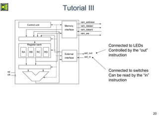
  • 20. 20 Tutorial III Connected to LEDs Controlled by the “out” instruction Connected to switches Can be read by the “in” instruction
  • 21. 21 Tutorial III • Let’s write a specific pattern of bits to the LEDs using the out instruction. Program: out 55h out aah out f0h out 0fh jmp 00 • Step 1: find the instruction encoding (in hex) 00 out 55h d055 02 out aah d0aa 04 out f0h d0f0 06 out 0fh d00f 08 jmp 00 b000
  • 22. 22 Tutorial III • Step 2: edit the memory • Step 3: execute – See the status of the LED 7..0 – Do the LED light up according to what you would expect? – Try the automatic clock (switch 23) – What happens when the program reaches address 08?
  • 23. 23 Exercise I • Consider the program below. Explain line by line the operation performed by the instruction and the resulting register values, for all registers that are used. xor ra,ra add ra,10h mov rb,11h sub ra,rb add ra,ra ror ra • You can program the processor with this program to see what it does!
  • 24. 24 Exercise II • This exercise will prepare you for one of the task in the coursework (but it is not identical to the coursework!) • Using the instruction summary sheet (available on StudyDirect under 'UoS processor doc') convert the following instructions given in hex into the human-readable assembler equivalent: AdrData ---------- 00 10 04 02 42 01 04 54 00 06 B1 10 08 22 00 0A C0 02 0C 34 01 0E B0 04 10 B0 10 12 63 00 14 3D 25 16 A0 03 • Attempt to understand the function of the program. • You can program the processor with this program to see what it does!
  • 25. 27 Alternative way to enter programs • The VHDL file ram.vhd contains the default startup state of the memory • By modifying ram.vhd a program can be placed in memory when the FPGA is programmed • Edit ram.vhd is useful for large programs and/or to keep past programs • Editing memory directly on the board is useful for quick modifications