


![cpe 252: Computer Organization 39
5-5 Instruction Cycle
Fetch and Decode cont.
– T0: AR←PC (this is essential!!)
The address of the instruction is moved to AR.
– T1: IR←M[AR], PC←PC+1
The instruction is fetched from the memory to IR
,
and the PC is incremented.
– T2: D0,…, D7←Decode IR(12-14), AR←IR(0-
11), I←IR(15)](https://image.slidesharecdn.com/chapter5new-200907163845/85/Basic-computer-organization-and-design-39-320.jpg)
![cpe 252: Computer Organization 40
BC Instruction cycle: [Fetch Decode [Indirect] Execute]*
• Fetch and Decode T0: AR PC (S0S1S2=010, T0=1)
T1: IR M [AR], PC PC + 1 (S0S1S2=111, T1=1)
T2: D0, . . . , D7 Decode IR(12-14), AR IR(0-11), I IR(15)
S2
S1
S0
Bus
7
Memory
unit
Address
Read
AR
LD
PC
INR
IR
LD Clock
1
2
5
Common bus
T1
T0](https://image.slidesharecdn.com/chapter5new-200907163845/85/Basic-computer-organization-and-design-40-320.jpg)
![cpe 252: Computer Organization 41
= 0 (direct)
D'7IT3: AR M[AR]
D'7I'T3: Nothing
D7I'T3: Execute a register-reference instr.
D7IT3: Execute an input-output instr.
Start
SC 0
AR PC
T0
IR M[AR], PC PC + 1
T1
AR IR(0-11), I IR(15)
Decode Opcode in IR(12-14),
T2
D7
= 0 (Memory-reference)(Register or I/O) = 1
II
Execute
register-reference
instruction
SC 0
Execute
input-output
instruction
SC 0
M[AR]AR Nothing
= 0 (register)(I/O) = 1 (indirect) = 1
T3 T3 T3 T3
Execute
memory-reference
instruction
SC 0
T4
DETERMINE THE TYPE OF INSTRUCTION](https://image.slidesharecdn.com/chapter5new-200907163845/85/Basic-computer-organization-and-design-41-320.jpg)

![cpe 252: Computer Organization 43
AND to AC
D0T4: DR M[AR] Read operand
D0T5: AC AC DR, SC 0 AND with AC
ADD to AC
D1T4: DR M[AR] Read operand
D1T5: AC AC + DR, E Cout, SC 0 Add to AC and store carry in E
- The effective address of the instruction is in AR and was placed there during
timing signal T2 when I = 0, or during timing signal T3 when I = 1
- Memory cycle is assumed to be short enough to be completed in a CPU cycle
- The execution of MR Instruction starts with T4
Symbol
Operation
Decoder
Symbolic Description
AND D0 AC AC M[AR]
ADD D1 AC AC + M[AR], E Cout
LDA D2 AC M[AR]
STA D3 M[AR] AC
BUN D4 PC AR
BSA D5 M[AR] PC, PC AR + 1
ISZ D6 M[AR] M[AR] + 1, if M[AR] + 1 = 0 then PC PC+1
5.6 MEMORY REFERENCE INSTRUCTIONS](https://image.slidesharecdn.com/chapter5new-200907163845/85/Basic-computer-organization-and-design-43-320.jpg)
![cpe 252: Computer Organization 44
MEMORY REFERENCE INSTRUCTIONScont.
Memory, PC after execution
21
0 BSA 135
Next instruction
Subroutine
20
Return address: PC = 21
AR = 135
136
1 BUN 135
Memory, PC, AR at time T4
0 BSA 135
Next instruction
Subroutine
20
21
135
PC = 136
1 BUN 135
Memory Memory
LDA: Load to AC
D2T4: DR M[AR]
D2T5: AC DR, SC 0
STA: Store AC
D3T4: M[AR] AC, SC 0
BUN: Branch Unconditionally
D4T4: PC AR, SC 0
BSA: Branch and Save Return Address
M[AR] PC, PC AR + 1](https://image.slidesharecdn.com/chapter5new-200907163845/85/Basic-computer-organization-and-design-44-320.jpg)
![cpe 252: Computer Organization 45
BSA: executed in a sequence of two micro-operations:
D5T4: M[AR] PC, AR AR + 1
D5T5: PC AR, SC 0
ISZ: Increment and Skip-if-Zero
D6T4: DR M[AR]
D6T5: DR DR + 1
D6T6: M[AR] DR, if (DR = 0) then (PC PC + 1), SC 0
Memory Reference
Instructionscont.](https://image.slidesharecdn.com/chapter5new-200907163845/85/Basic-computer-organization-and-design-45-320.jpg)
![cpe 252: Computer Organization 46
Memory-reference instruction
DR M[AR] DR M[AR] DR M[AR] M[AR] AC
SC 0
AND ADD LDA STA
AC AC DR
SC <- 0
AC AC + DR
E Cout
SC 0
AC DR
SC 0
D T0 4 D T1 4 D T2 4 D T3 4
D T0 5 D T1 5 D T2 5
PC AR
SC 0
M[AR] PC
AR AR + 1
DR M[AR]
BUN BSA ISZ
D T4 4 D T5 4 D T6 4
DR DR + 1
D T5 5 D T6 5
PC AR
SC 0
M[AR] DR
If (DR = 0)
then (PC PC + 1)
SC 0
D T6 6
](https://image.slidesharecdn.com/chapter5new-200907163845/85/Basic-computer-organization-and-design-46-320.jpg)


![cpe 252: Computer Organization 63
IEN
=0
=1
Program Interruptcont.
R = Interrupt flip-flop
Store return address
=1=0
in location 0
M[0] PC
Branch to location 1
PC 1
IEN 0
R 0
Interrupt cycleInstruction cycle
Fetch and decode
instructions
Execute
instructions
R 1
=1
=1
=0
=0
FGI
FGO
R
Flowchart for interrupt cycle](https://image.slidesharecdn.com/chapter5new-200907163845/85/Basic-computer-organization-and-design-63-320.jpg)


![cpe 252: Computer Organization 66
Interrupt Cycle
• The fetch and decode phases of the
instruction cycle must be :
(Replace T0, T1, T2 R'T0, R'T1, R'T2
(fetch and decode phases occur at the
instruction cycle when R = 0)
• Interrupt Cycle:
– RT0: AR 0, TR PC
– RT1: M[AR] TR, PC 0
– RT2: PC PC + 1, IEN 0, R 0, SC 0](https://image.slidesharecdn.com/chapter5new-200907163845/85/Basic-computer-organization-and-design-66-320.jpg)


![cpe 252: Computer Organization 69
AR M[AR]Execute
RR
Instruction
Execute
I/O
Instruction
I
PC PC + 1, IEN 0
R 0, SC 0
D7
AR IR(0~11), I IR(15)
D0...D7 Decode IR(12 ~ 14)
M[AR] TR, PC 0IR M[AR], PC PC + 1
AR 0, TR PCAR PC
R
start
SC 0, IEN 0, R 0
5-8 Complete Computer Description
(I/O) =1 =0 (Register) (Indir) =1 =0 (Dir)
R’T0
R’T1
R’T2
RT0
RT1
RT2
I
Idle
D7IT3 D7I’T3 D7’IT3 D7’I’T3
Execute MR
Instruction
(Instruction Cycle) =0 =1 (Interrupt Cycle)
(Register or I/O) =1 =0 (Memory Ref)
D7’T4
Fig 5-15](https://image.slidesharecdn.com/chapter5new-200907163845/85/Basic-computer-organization-and-design-69-320.jpg)
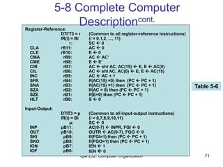
![cpe 252: Computer Organization 70
AR PC
IR M[AR], PC PC + 1
D0, ..., D7 Decode IR(12 ~ 14), AR IR(0 ~ 11), I IR(15)
AR M[AR]
R 1
AR 0, TR PC
M[AR] TR, PC 0
PC PC + 1, IEN 0, R 0, SC 0
DR M[AR]
AC AC . DR, SC 0
DR M[AR]
AC AC + DR, E Cout, SC 0
DR M[AR]
AC DR, SC 0
M[AR] AC, SC 0
PC AR, SC 0
M[AR] PC, AR AR + 1
PC AR, SC 0
DR M[AR]
DR DR + 1
M[AR] DR, if(DR=0) then (PC PC + 1), SC 0
5-8 Complete Computer
Descriptioncont.
Fetch
Decode
Indirect
Interrupt:
Memory-Reference:
AND
ADD
LDA
STA
BUN
BSA
ISZ
R’T0:
R’T1:
R’T2:
D7’IT3:
RT0:
RT1:
RT2:
D0T4:
D0T5:
D1T4:
D1T5:
D2T4:
D2T5:
D3T4:
D4T4:
D5T4:
D5T5:
D6T4:
D6T5:
D6T6:
T0’T1’T2’(IEN)(FGI + FGO):](https://image.slidesharecdn.com/chapter5new-200907163845/85/Basic-computer-organization-and-design-70-320.jpg)


![cpe 252: Computer Organization 74
5-9 Design of Basic
Computercont.
• Control of registers and memory
– The control inputs of the registers are LD
(load), INR (increment), and CLR (clear)
– To control AR We scan table 5-6 to find out
all the statements that change the content of
AR:
• R’T0: AR PC LD(AR)
• R’T2: AR IR(0-11) LD(AR)
• D’7IT3: AR M[AR] LD(AR)
• RT0: AR 0 CLR(AR)
• D5T4: AR AR + 1 INR(AR)](https://image.slidesharecdn.com/chapter5new-200907163845/85/Basic-computer-organization-and-design-74-320.jpg)

![cpe 252: Computer Organization 76
5-9 Design of Basic
Computercont.
– To control the Read input of the memory we
scan the table again to get these:
• D0T4: DR M[AR]
• D1T4: DR M[AR]
• D2T4: DR M[AR]
• D6T4: DR M[AR]
• D7′IT3: AR M[AR]
• R′T1: IR M[AR]
– Read = R′T1 + D7′IT3 + (D0 + D1 + D2 + D6 )T4](https://image.slidesharecdn.com/chapter5new-200907163845/85/Basic-computer-organization-and-design-76-320.jpg)


Basic computer organization and design
- 1. cpe 252: Computer Organization 1 Basic Computer Organization and Design Chapter 5:
- 2. cpe 252: Computer Organization 2 5-1 Instruction Codes • The Internal organization of a digital system is defined by the sequence of microoperations it performs on data stored in its registers • The user of a computer can control the process by means of a program • A program is a set of instructions that specify the operations, operands, and the processing sequence
- 3. cpe 252: Computer Organization 3 5-1 Instruction Codes cont. • A computer instruction is a binary code that specifies a sequence of micro-operations for the computer. Each computer has its unique instruction set • Instruction codes and data are stored in memory • The computer reads each instruction from memory and places it in a control register • The control unit interprets the binary code of the instruction and proceeds to execute it by issuing a sequence of micro-operations
- 4. cpe 252: Computer Organization 4 5-1 Instruction Codes cont. • An Instruction code is a group of bits that instructs the computer to perform a specific operation (sequence of microoperations). It is divided into parts (basic part is the operation part) • The operation code of an instruction is a group of bits that defines certain operations such as add, subtract, shift, and complement
- 5. cpe 252: Computer Organization 5 5-1 Instruction Codes cont. • The number of bits required for the operation code depends on the total number of operations available in the computer • 2n (or little less) distinct operations n bit operation code
- 6. cpe 252: Computer Organization 6 5-1 Instruction Codes cont. 110010?????????? Op code Control Unit Read instruction from memory It’s an ADD operation Memory
- 7. cpe 252: Computer Organization 7 5-1 Instruction Codes cont. • An operation must be performed on some data stored in processor registers or in memory • An instruction code must therefore specify not only the operation, but also the location of the operands (in registers or in the memory), and where the result will be stored (registers/memory)
- 8. cpe 252: Computer Organization 8 5-1 Instruction Codes cont. • Memory words can be specified in instruction codes by their address • Processor registers can be specified by assigning to the instruction another binary code of k bits that specifies one of 2k registers • Each computer has its own particular instruction code format • Instruction code formats are conceived by computer designers who specify the architecture of the computer
- 9. cpe 252: Computer Organization 9 5-1 Instruction Codes cont. Stored Program Organization • An instruction code is usually divided into operation code, operand address, addressing mode, etc. • The simplest way to organize a computer is to have one processor register (accumulator AC) and an instruction code format with two parts (op code, address)
- 10. cpe 252: Computer Organization 10 5-1 Instruction Codes Stored Program Organization cont. Opcode Address Instruction Format Binary Operand Operands (data) Processor register (Accumulator AC) Memory 4096x16 15 12 11 0 15 0 Instructions (program) 15 0 015
- 11. cpe 252: Computer Organization 11 5-1 Instruction Codes Indirect Address • There are three Addressing Modes used for address portion of the instruction code: – Direct: the address points to the operand stored in the memory – Indirect: the address points to the pointer (another address) stored in the memory that references the operand in memory • One bit of the instruction code can be used to distinguish between direct & indirect addresses
- 12. cpe 252: Computer Organization 12 5-1 Instruction Codes Indirect Address cont. Opcode Address Instruction Format 15 14 12 0 I 11 0 ADD 45722 Operand457 1 ADD 30035 1350300 Operand1350 + AC + AC Direct Address Indirect address Effective address
- 13. cpe 252: Computer Organization 13 5-1 Instruction Codes Indirect Address cont. • Effective address: the address of the operand in a computation-type instruction or the target address in a branch-type instruction • The pointer can be placed in a processor register instead of memory as done in commercial computers
- 14. cpe 252: Computer Organization 14 5-2 Computer Registers • Computer instructions are normally stored in consecutive memory locations and executed sequentially one at a time • The control reads an instruction from a specific address in memory and executes it, and so on • This type of sequencing needs a counter to calculate the address of the next instruction after execution of the current instruction is completed
- 15. cpe 252: Computer Organization 15 5-2 Computer Registers cont. • It is also necessary to provide a register in the control unit for storing the instruction code after it is read from memory • The computer needs processor registers for manipulating data and a register for holding a memory address
- 16. cpe 252: Computer Organization 16 In order to cover the basic concepts behind designing a computer, a model (an imaginary system) will be presented to you throughout this chapter. This model will be called the “Basic Computer”
- 17. cpe 252: Computer Organization 17 List of BC Registers DR 16 Data Register Holds memory operand AR 12 Address Register Holds address for memory AC 16 Accumulator Processor register IR 16 Instruction Register Holds instruction code PC 12 Program Counter Holds address of instruction TR 16 Temporary Register Holds temporary data INPR 8 Input Register Holds input character OUTR 8 Output Register Holds output character Registers in the Basic Computer 11 0 PC 15 0 IR 15 0 TR 7 0 OUTR 15 0 DR 15 0 AC 11 0 AR INPR 0 7 Memory 4096 x 16
- 18. cpe 252: Computer Organization 18 S2 S1 S0 Bus Memory unit 4096 x 16 LD INR CLR Address ReadWrite AR LD INR CLR PC LD INR CLR DR LD INR CLR AC Adder and logic E INPR IR LD LD INR CLR TR OUTR LD Clock 16-bit common bus 7 1 2 3 4 5 6 Computer Registers Common Bus System
- 19. cpe 252: Computer Organization 19 5-2 Computer Registers Common Bus System cont. • S2S1S0: Selects the register/memory that would use the bus • LD (load): When enabled, the particular register receives the data from the bus during the next clock pulse transition • E (extended AC bit): flip-flop holds the carry • DR, AC, IR, and TR: have 16 bits each • AR and PC: have 12 bits each since they hold a memory address
- 20. cpe 252: Computer Organization 20 5-2 Computer Registers Common Bus System cont. • When the contents of AR or PC are applied to the 16-bit common bus, the four most significant bits are set to zeros • When AR or PC receives information from the bus, only the 12 least significant bits are transferred into the register • INPR and OUTR: communicate with the eight least significant bits in the bus
- 21. cpe 252: Computer Organization 21 5-2 Computer Registers Common Bus System cont. • INPR: Receives a character from the input device (keyboard,…etc) which is then transferred to AC • OUTR: Receives a character from AC and delivers it to an output device (say a Monitor) • Five registers have three control inputs: LD (load), INR (increment), and CLR (clear) • Register binary counter with parallel load and synchronous clear
- 22. cpe 252: Computer Organization 22 5-2 Computer Registers Memory Address • The input data and output data of the memory are connected to the common bus • But the memory address is connected to AR • Therefore, AR must always be used to specify a memory address • By using a single register for the address, we eliminate the need for an address bus that would have been needed otherwise
- 23. cpe 252: Computer Organization 23 5-2 Computer Registers Memory Address cont. • Register Memory: Write operation • Memory Register: Read operation (note that AC cannot directly read from memory!!) • Note that the content of any register can be applied onto the bus and an operation can be performed in the adder and logic circuit during the same clock cycle
- 24. cpe 252: Computer Organization 24 5-2 Computer Registers Memory Address cont. • The transition at the end of the cycle transfers the content of the bus into the destination register, and the output of the adder and logic circuit into the AC • For example, the two microoperations DR←AC and AC←DR (Exchange) can be executed at the same time • This is done by:
- 25. cpe 252: Computer Organization 25 5-2 Computer Registers Memory Address cont. • 1- place the contents of AC on the bus (S2S1S0=100) • 2- enabling the LD (load) input of DR • 3- Transferring the contents of the DR through the adder and logic circuit into AC • 4- enabling the LD (load) input of AC • All during the same clock cycle • The two transfers occur upon the arrival of the clock pulse transition at the end of the clock cycle
- 26. cpe 252: Computer Organization 26 Memory-Reference Instructions (OP-code = 000 ~ 110) 5-3 Computer Instructions Basic Computer Instruction code format 15 14 12 11 0 I Opcode Address Register-Reference Instructions (OP-code = 111, I = 0) Input-Output Instructions (OP-code =111, I = 1) 15 12 11 0 Register operation0 1 1 1 15 12 11 0 I/O operation1 1 1 1
- 27. cpe 252: Computer Organization 27 BASIC COMPUTER INSTRUCTIONS Hex Code Symbol I = 0 I = 1 Description AND 0xxx 8xxx AND memory word to AC ADD 1xxx 9xxx Add memory word to AC LDA 2xxx Axxx Load AC from memory STA 3xxx Bxxx Store content of AC into memory BUN 4xxx Cxxx Branch unconditionally BSA 5xxx Dxxx Branch and save return address ISZ 6xxx Exxx Increment and skip if zero CLA 7800 Clear AC CLE 7400 Clear E CMA 7200 Complement AC CME 7100 Complement E CIR 7080 Circulate right AC and E CIL 7040 Circulate left AC and E INC 7020 Increment AC SPA 7010 Skip next instr. if AC is positive SNA 7008 Skip next instr. if AC is negative SZA 7004 Skip next instr. if AC is zero SZE 7002 Skip next instr. if E is zero HLT 7001 Halt computer INP F800 Input character to AC OUT F400 Output character from AC SKI F200 Skip on input flag SKO F100 Skip on output flag ION F080 Interrupt on IOF F040 Interrupt off
- 28. cpe 252: Computer Organization 28 5-3 Computer Instructions Instruction Set Completeness • The set of instructions are said to be complete if the computer includes a sufficient number of instructions in each of the following categories: – Arithmetic, logical, and shift instructions – Instructions for moving information to and from memory and processor registers – Program control instructions together with instructions that check status conditions – Input & output instructions
- 29. cpe 252: Computer Organization 29 5-4 Timing & Control • The timing for all registers in the basic computer is controlled by a master clock generator • The clock pulses are applied to all flip- flops and registers in the system, including the flip-flops and registers in the control unit • The clock pulses do not change the state of a register unless the register is enabled by a control signal (i.e., Load)
- 30. cpe 252: Computer Organization 30 5-4 Timing & Control cont. • The control signals are generated in the control unit and provide control inputs for the multiplexers in the common bus, control inputs in processor registers, and microoperations for the accumulator • There are two major types of control organization: – Hardwired control – Microprogrammed control
- 31. cpe 252: Computer Organization 31 5-4 Timing & Control cont. • In the hardwired organization, the control logic is implemented with gates, flip-flops, decoders, and other digital circuits. • In the microprogrammed organization, the control information is stored in a control memory (if the design is modified, the microprogram in control memory has to be updated) • D3T4: SC←0
- 32. cpe 252: Computer Organization 32 I The Control Unit for the basic computer Hardwired Control Organization Instruction register (IR) 15 14 13 12 11 - 0 3 x 8 decoder 7 6 5 4 3 2 1 0 Control logic gates D0 15 14 . . . . 2 1 0 4 x 16 Sequence decoder 4-bit sequence counter (SC) Increment (INR) Clear (CLR) Clock Other inputs Control outputs D T T 7 15 0
- 33. cpe 252: Computer Organization 33 Clock T0 T1 T2 T3 T4 T0 T0 T1 T2 T3 T4 D3 CLR SC - Generated by 4-bit sequence counter and 4x16 decoder - The SC can be incremented or cleared. - Example: T0, T1, T2, T3, T4, T0, T1, . . . Assume: At time T4, SC is cleared to 0 if decoder output D3 is active. D3T4: SC 0
- 34. cpe 252: Computer Organization 34 5-4 Timing & Control cont. • A memory read or write cycle will be initiated with the rising edge of a timing signal • Assume: memory cycle time < clock cycle time! • So, a memory read or write cycle initiated by a timing signal will be completed by the time the next clock goes through its positive edge • The clock transition will then be used to load the memory word into a register • The memory cycle time is usually longer than the processor clock cycle wait cycles
- 35. cpe 252: Computer Organization 35 5-4 Timing & Control cont. • T0: AR←PC – Transfers the content of PC into AR if timing signal T0 is active – T0 is active during an entire clock cycle interval – During this time, the content of PC is placed onto the bus (with S2S1S0=010) and the LD (load) input of AR is enabled – The actual transfer does not occur until the end of the clock cycle when the clock goes through a positive transition – This same positive clock transition increments the sequence counter SC from 0000 to 0001 – The next clock cycle has T1 active and T0 inactive
- 36. cpe 252: Computer Organization 36 5-5 Instruction Cycle • A program is a sequence of instructions stored in memory • The program is executed in the computer by going through a cycle for each instruction (in most cases) • Each instruction in turn is subdivided into a sequence of sub-cycles or phases
- 37. cpe 252: Computer Organization 37 5-5 Instruction Cycle cont. • Instruction Cycle Phases: – 1- Fetch an instruction from memory – 2- Decode the instruction – 3- Read the effective address from memory if the instruction has an indirect address – 4- Execute the instruction • This cycle repeats indefinitely unless a HALT instruction is encountered
- 38. cpe 252: Computer Organization 38 5-5 Instruction Cycle Fetch and Decode • Initially, the Program Counter (PC) is loaded with the address of the first instruction in the program • The sequence counter SC is cleared to 0, providing a decoded timing signal T0 • After each clock pulse, SC is incremented by one, so that the timing signals go through a sequence T0, T1, T2, and so on
- 39. cpe 252: Computer Organization 39 5-5 Instruction Cycle Fetch and Decode cont. – T0: AR←PC (this is essential!!) The address of the instruction is moved to AR. – T1: IR←M[AR], PC←PC+1 The instruction is fetched from the memory to IR , and the PC is incremented. – T2: D0,…, D7←Decode IR(12-14), AR←IR(0- 11), I←IR(15)
- 40. cpe 252: Computer Organization 40 BC Instruction cycle: [Fetch Decode [Indirect] Execute]* • Fetch and Decode T0: AR PC (S0S1S2=010, T0=1) T1: IR M [AR], PC PC + 1 (S0S1S2=111, T1=1) T2: D0, . . . , D7 Decode IR(12-14), AR IR(0-11), I IR(15) S2 S1 S0 Bus 7 Memory unit Address Read AR LD PC INR IR LD Clock 1 2 5 Common bus T1 T0
- 41. cpe 252: Computer Organization 41 = 0 (direct) D'7IT3: AR M[AR] D'7I'T3: Nothing D7I'T3: Execute a register-reference instr. D7IT3: Execute an input-output instr. Start SC 0 AR PC T0 IR M[AR], PC PC + 1 T1 AR IR(0-11), I IR(15) Decode Opcode in IR(12-14), T2 D7 = 0 (Memory-reference)(Register or I/O) = 1 II Execute register-reference instruction SC 0 Execute input-output instruction SC 0 M[AR]AR Nothing = 0 (register)(I/O) = 1 (indirect) = 1 T3 T3 T3 T3 Execute memory-reference instruction SC 0 T4 DETERMINE THE TYPE OF INSTRUCTION
- 42. cpe 252: Computer Organization 42 REGISTER REFERENCE INSTRUCTIONS r = D7 I’ T3 => Register Reference Instruction Bi = IR(i) , i=0,1,2,...,11, the ith bit of IR. - D7 = 1, I = 0 - Register Ref. Instr. is specified in B0 ~ B11 of IR - Execution starts with timing signal T3 Register Reference Instructions are identified when r: SC 0 CLA rB11: AC 0 CLE rB10: E 0 CMA rB9: AC AC’ CME rB8: E E’ CIR rB7: AC shr AC, AC(15) E, E AC(0) CIL rB6: AC shl AC, AC(0) E, E AC(15) INC rB5: AC AC + 1 SPA rB4: if (AC(15) = 0) then (PC PC+1) SNA rB3: if (AC(15) = 1) then (PC PC+1) SZA rB2: if (AC = 0) then (PC PC+1) SZE rB1: if (E = 0) then (PC PC+1) HLT rB0: S 0 (S is a start-stop flip-flop)
- 43. cpe 252: Computer Organization 43 AND to AC D0T4: DR M[AR] Read operand D0T5: AC AC DR, SC 0 AND with AC ADD to AC D1T4: DR M[AR] Read operand D1T5: AC AC + DR, E Cout, SC 0 Add to AC and store carry in E - The effective address of the instruction is in AR and was placed there during timing signal T2 when I = 0, or during timing signal T3 when I = 1 - Memory cycle is assumed to be short enough to be completed in a CPU cycle - The execution of MR Instruction starts with T4 Symbol Operation Decoder Symbolic Description AND D0 AC AC M[AR] ADD D1 AC AC + M[AR], E Cout LDA D2 AC M[AR] STA D3 M[AR] AC BUN D4 PC AR BSA D5 M[AR] PC, PC AR + 1 ISZ D6 M[AR] M[AR] + 1, if M[AR] + 1 = 0 then PC PC+1 5.6 MEMORY REFERENCE INSTRUCTIONS
- 44. cpe 252: Computer Organization 44 MEMORY REFERENCE INSTRUCTIONScont. Memory, PC after execution 21 0 BSA 135 Next instruction Subroutine 20 Return address: PC = 21 AR = 135 136 1 BUN 135 Memory, PC, AR at time T4 0 BSA 135 Next instruction Subroutine 20 21 135 PC = 136 1 BUN 135 Memory Memory LDA: Load to AC D2T4: DR M[AR] D2T5: AC DR, SC 0 STA: Store AC D3T4: M[AR] AC, SC 0 BUN: Branch Unconditionally D4T4: PC AR, SC 0 BSA: Branch and Save Return Address M[AR] PC, PC AR + 1
- 45. cpe 252: Computer Organization 45 BSA: executed in a sequence of two micro-operations: D5T4: M[AR] PC, AR AR + 1 D5T5: PC AR, SC 0 ISZ: Increment and Skip-if-Zero D6T4: DR M[AR] D6T5: DR DR + 1 D6T6: M[AR] DR, if (DR = 0) then (PC PC + 1), SC 0 Memory Reference Instructionscont.
- 46. cpe 252: Computer Organization 46 Memory-reference instruction DR M[AR] DR M[AR] DR M[AR] M[AR] AC SC 0 AND ADD LDA STA AC AC DR SC <- 0 AC AC + DR E Cout SC 0 AC DR SC 0 D T0 4 D T1 4 D T2 4 D T3 4 D T0 5 D T1 5 D T2 5 PC AR SC 0 M[AR] PC AR AR + 1 DR M[AR] BUN BSA ISZ D T4 4 D T5 4 D T6 4 DR DR + 1 D T5 5 D T6 5 PC AR SC 0 M[AR] DR If (DR = 0) then (PC PC + 1) SC 0 D T6 6
- 47. cpe 252: Computer Organization 47 5-7 Input-Output and Interrupt • Instructions and data stored in memory must come from some input device • Computational results must be transmitted to the user through some output device • For the system to communicate with an input device, serial information is shifted into the input register INPR • To output information, it is stored in the output register OUTR
- 48. cpe 252: Computer Organization 48 5-7 Input-Output and Interruptcont. Input-output terminal Serial communication interface Computer registers and flip-flops Printer Keyboard Receiver interface Transmitter interface FGOOUTR AC INPR FGI Serial Communications Path Parallel Communications Path
- 49. cpe 252: Computer Organization 49 5-7 Input-Output and Interruptcont. • INPR and OUTR communicate with a communication interface serially and with the AC in parallel. They hold an 8-bit alphanumeric information • I/O devices are slower than a computer system we need to synchronize the timing rate difference between the input/output device and the computer. • FGI: 1-bit input flag (Flip-Flop) aimed to control the input operation
- 50. cpe 252: Computer Organization 50 5-7 Input-Output and Interrupt cont. • FGI is set to 1 when a new information is available in the input device and is cleared to 0 when the information is accepted by the computer • FGO: 1-bit output flag used as a control flip-flop to control the output operation • If FGO is set to 1, then this means that the computer can send out the information from AC. If it is 0, then the output device is busy and the computer has to wait!
- 51. cpe 252: Computer Organization 51 5-7 Input-Output and Interruptcont. • The process of input information transfer: – Initially, FGI is cleared to 0 – An 8-bit alphanumeric code is shifted into INPR (Keyboard key strike) and the input flag FGI is set to 1 – As long as the flag is set, the information in INPR cannot be changed by another data entry – The computer checks the flag bit; if it is 1, the information from INPR is transferred in parallel into AC and FGI is cleared to 0
- 52. cpe 252: Computer Organization 52 5-7 Input-Output and Interruptcont. – Once the flag is cleared, new information can be shifted into INPR by the input device (striking another key) • The process of outputting information: – Initially, the output flag FGO is set to 1 – The computer checks the flag bit; if it is 1, the information from AC is transferred in parallel to OUTR and FGO is cleared to 0 – The output accepts the coded information (prints the corresponding character)
- 53. cpe 252: Computer Organization 53 5-7 Input-Output and Interruptcont. – When the operation is completed, the output device sets FGO back to 1 – The computer does not load a new data information into OUTR when FGO is 0 because this condition indicates that the output device is busy to receive another information at the moment!!
- 54. cpe 252: Computer Organization 54 Input-Output Instructions • Needed for: – Transferring information to and from AC register – Checking the flag bits – Controlling the interrupt facility • The control unit recognize it when D7=1 and I = 1 • The remaining bits of the instruction specify the particular operation • Executed with the clock transition associated with timing signal T3 • Input-Output instructions are summarized next
- 55. cpe 252: Computer Organization 55 D7IT3 = p IR(i) = Bi, i = 6, …, 11 INP pB11: AC(0-7) INPR, FGI 0 Input char. to AC OUT pB10: OUTR AC(0-7), FGO 0 Output char. from AC SKI pB9: if(FGI = 1) then (PC PC + 1) Skip on input flag SKO pB8: if(FGO = 1) then (PC PC + 1) Skip on output flag ION pB7: IEN 1 Interrupt enable on IOF pB6: IEN 0 Interrupt enable off Input-Output Instructions
- 56. cpe 252: Computer Organization 56 Program Interrupt • The process of communication just described is referred to as Programmed Control Transfer • The computer keeps checking the flag bit, and when it finds it set, it initiates an information transform (this is sometimes called Polling) • This type of transfer is in-efficient due to the difference of information flow rate between the computer and the I/O device
- 57. cpe 252: Computer Organization 57 Program Interruptcont. • The computer is wasting time while checking the flag instead of doing some other useful processing task • An alternative to the programmed controlled procedure is to let the external device inform the computer when it is ready for the transfer • This type of transfer uses the interrupt facility
- 58. cpe 252: Computer Organization 58 Program Interruptcont. • While the computer is running a program, it does not check the flags • Instead: – When a flag is set, the computer is immediately interrupted from proceeding with the current program
- 59. cpe 252: Computer Organization 59 Program Interruptcont. – The computer stops what it is doing to take care of the input or output transfer – Then, it returns to the current program to continue what it was doing before the interrupt • The interrupt facility can be enabled or disabled via a flip-flop called IEN • The interrupt enable flip-flop IEN can be set and cleared with two instructions (IOF, ION): – IOF: IEN 0 (the computer cannot be interrupted) – ION: IEN 1 (the computer can be interrupted)
- 60. cpe 252: Computer Organization 60 Program Interruptcont. • Another flip-flop (called the interrupt flip- flop R) is used in the computer’s interrupt facility to decide when to go through the interrupt cycle • FGI and FGO are different here compared to the way they acted in an earlier discussion!! • So, the computer is either in an Instruction Cycle or in an Interrupt Cycle
- 61. cpe 252: Computer Organization 61 Program Interruptcont. • The interrupt cycle is a hardware implementation of a branch and save return address operation (BSA) • The return address available in PC is stored in a specific location where it can be found later when the program returns to the instruction at which it was interrupted • This location may be a processor register, a memory stack, or a specific memory location
- 62. cpe 252: Computer Organization 62 Program Interruptcont. • For our computer, we choose the memory location at address 0 as a place for storing the return address • Control then inserts address 1 into PC: this means that the first instruction of the interrupt service routine should be stored in memory at address 1, or, the programmer must store a branch instruction that sends the control to an interrupt service routine!!
- 63. cpe 252: Computer Organization 63 IEN =0 =1 Program Interruptcont. R = Interrupt flip-flop Store return address =1=0 in location 0 M[0] PC Branch to location 1 PC 1 IEN 0 R 0 Interrupt cycleInstruction cycle Fetch and decode instructions Execute instructions R 1 =1 =1 =0 =0 FGI FGO R Flowchart for interrupt cycle
- 64. cpe 252: Computer Organization 64 Program Interruptcont. • IEN, R 0: no more interruptions can occur until the interrupt request from the flag has been serviced • The service routine must end with an instruction that re-enables the interrupt (IEN 1) and an instruction to return to the instruction at which the interrupt occurred • The instruction that returns the control to the original program is "indirect BUN 0"
- 65. cpe 252: Computer Organization 65 Program Interruptcont. • Example: the computer is interrupted during execution of the instruction at address 255 After interrupt cycle 0 BUN 1120 0 1 PC = 256 255 1 BUN 0 Before interrupt Main Program 1120 I/O Program 0 BUN 1120 0 PC = 1 256 255 1 BUN 0 Memory Main Program 1120 I/O Program 256
- 66. cpe 252: Computer Organization 66 Interrupt Cycle • The fetch and decode phases of the instruction cycle must be : (Replace T0, T1, T2 R'T0, R'T1, R'T2 (fetch and decode phases occur at the instruction cycle when R = 0) • Interrupt Cycle: – RT0: AR 0, TR PC – RT1: M[AR] TR, PC 0 – RT2: PC PC + 1, IEN 0, R 0, SC 0
- 67. CPE252 cpe 252: Computer Organization 67 + AR CLR PC CLR INR TR LD Memory write K J K J S0 S1 S2 2 6 1 7 16-bit common bus 0 0 0 Clock IEN R R T0 T1 T2 SCCLR Address Register transfers for the Interrupt Cycle
- 68. cpe 252: Computer Organization 68 Interrupt cont. • Further Questions: – How can the CPU recognize the device requesting an interrupt? – Since different devices are likely to require different interrupt service routines, how can the CPU obtain the starting address of the appropriate routine in each case? – Should any device be allowed to interrupt the CPU while another interrupt is being serviced? – How can the situation be handled when two or more interrupt requests occur simultaneously?
- 69. cpe 252: Computer Organization 69 AR M[AR]Execute RR Instruction Execute I/O Instruction I PC PC + 1, IEN 0 R 0, SC 0 D7 AR IR(0~11), I IR(15) D0...D7 Decode IR(12 ~ 14) M[AR] TR, PC 0IR M[AR], PC PC + 1 AR 0, TR PCAR PC R start SC 0, IEN 0, R 0 5-8 Complete Computer Description (I/O) =1 =0 (Register) (Indir) =1 =0 (Dir) R’T0 R’T1 R’T2 RT0 RT1 RT2 I Idle D7IT3 D7I’T3 D7’IT3 D7’I’T3 Execute MR Instruction (Instruction Cycle) =0 =1 (Interrupt Cycle) (Register or I/O) =1 =0 (Memory Ref) D7’T4 Fig 5-15
- 70. cpe 252: Computer Organization 70 AR PC IR M[AR], PC PC + 1 D0, ..., D7 Decode IR(12 ~ 14), AR IR(0 ~ 11), I IR(15) AR M[AR] R 1 AR 0, TR PC M[AR] TR, PC 0 PC PC + 1, IEN 0, R 0, SC 0 DR M[AR] AC AC . DR, SC 0 DR M[AR] AC AC + DR, E Cout, SC 0 DR M[AR] AC DR, SC 0 M[AR] AC, SC 0 PC AR, SC 0 M[AR] PC, AR AR + 1 PC AR, SC 0 DR M[AR] DR DR + 1 M[AR] DR, if(DR=0) then (PC PC + 1), SC 0 5-8 Complete Computer Descriptioncont. Fetch Decode Indirect Interrupt: Memory-Reference: AND ADD LDA STA BUN BSA ISZ R’T0: R’T1: R’T2: D7’IT3: RT0: RT1: RT2: D0T4: D0T5: D1T4: D1T5: D2T4: D2T5: D3T4: D4T4: D5T4: D5T5: D6T4: D6T5: D6T6: T0’T1’T2’(IEN)(FGI + FGO):
- 71. cpe 252: Computer Organization 71 5-8 Complete Computer Descriptioncont. Register-Reference: CLA CLE CMA CME CIR CIL INC SPA SNA SZA SZE HLT Input-Output: INP OUT SKI SKO ION IOF D7I’T3 = r IR(i) = Bi r: rB11: rB10: rB9: rB8: rB7: rB6: rB5: rB4: rB3: rB2: rB1: rB0: D7IT3 = p IR(i) = Bi p: pB11: pB10: pB9: pB8: pB7: pB6: (Common to all register-reference instructions) (i = 0,1,2, ..., 11) SC 0 AC 0 E 0 AC AC’ E E’ AC shr AC, AC(15) E, E AC(0) AC shl AC, AC(0) E, E AC(15) AC AC + 1 If(AC(15) =0) then (PC PC + 1) If(AC(15) =1) then (PC PC + 1) If(AC = 0) then (PC PC + 1) If(E=0) then (PC PC + 1) S 0 (Common to all input-output instructions) (i = 6,7,8,9,10,11) SC 0 AC(0-7) INPR, FGI 0 OUTR AC(0-7), FGO 0 If(FGI=1) then (PC PC + 1) If(FGO=1) then (PC PC + 1) IEN 1 IEN 0 Table 5-6
- 72. cpe 252: Computer Organization 72 5-9 Design of Basic Computer 1. A memory unit: 4096 x 16. 2. Registers: AR, PC, DR, AC, IR, TR, OUTR, INPR, and SC 3. Flip-Flops (Status): I, S, E, R, IEN, FGI, and FGO 4. Decoders: 1. a 3x8 Opcode decoder 2. a 4x16 timing decoder 5. Common bus: 16 bits 6. Control logic gates 7. Adder and Logic circuit: Connected to AC
- 73. cpe 252: Computer Organization 73 5-9 Design of Basic Computercont. • The control logic gates are used to control: – Inputs of the nine registers – Read and Write inputs of memory – Set, Clear, or Complement inputs of the flip- flops – S2, S1, S0 that select a register for the bus – AC Adder and Logic circuit
- 74. cpe 252: Computer Organization 74 5-9 Design of Basic Computercont. • Control of registers and memory – The control inputs of the registers are LD (load), INR (increment), and CLR (clear) – To control AR We scan table 5-6 to find out all the statements that change the content of AR: • R’T0: AR PC LD(AR) • R’T2: AR IR(0-11) LD(AR) • D’7IT3: AR M[AR] LD(AR) • RT0: AR 0 CLR(AR) • D5T4: AR AR + 1 INR(AR)
- 75. cpe 252: Computer Organization 75 5-9 Design of Basic Computercont. AR LD INR CLR Clock To busFrom bus D' I T T R T D5 T 7 3 2 0 4 Control Gates associated with AR
- 76. cpe 252: Computer Organization 76 5-9 Design of Basic Computercont. – To control the Read input of the memory we scan the table again to get these: • D0T4: DR M[AR] • D1T4: DR M[AR] • D2T4: DR M[AR] • D6T4: DR M[AR] • D7′IT3: AR M[AR] • R′T1: IR M[AR] – Read = R′T1 + D7′IT3 + (D0 + D1 + D2 + D6 )T4
- 77. cpe 252: Computer Organization 77 5-9 Design of Basic Computercont. • Control of Single Flip-flops (IEN for example) – pB7: IEN 1 (I/O Instruction) – pB6: IEN 0 (I/O Instruction) – RT2: IEN 0 (Interrupt) • where p = D7IT3 (Input/Output Instruction) – If we use a JK flip-flop for IEN, the control gate logic will be as shown in the following slide:
- 78. cpe 252: Computer Organization 78 5-9 Design of Basic Computercont. D I T3 7 J K Q IEN p B7 B6 T2 R J K Q(t+1) 0 0 Q(t) 0 1 0 1 0 1 1 1 Q’(t) JK FF Characteristic Table
- 79. cpe 252: Computer Organization 79 5-9 Design of Basic Computercont. • Control of Common bus is accomplished by placing an encoder at the inputs of the bus selection logic and implementing the logic for each encoder input x1 x2 x3 x4 x5 x6 x7 Encoder S 2 S 1 S 0 Multiplexer bus select inputs
- 80. cpe 252: Computer Organization 80 5-9 Design of Basic Computercont. • To select AR on the bus then x1 must be 1. This is happen when: • D4T4: PC AR • D5T5: PC AR • x1 = D4T4 + D5T5 x1 x2 x3 x4 x5 x6 x7 S2 S1 S0 selected register 0 0 0 0 0 0 0 0 0 0 none 1 0 0 0 0 0 0 0 0 1 AR 0 1 0 0 0 0 0 0 1 0 PC 0 0 1 0 0 0 0 0 1 1 DR 0 0 0 1 0 0 0 1 0 0 AC 0 0 0 0 1 0 0 1 0 1 IR 0 0 0 0 0 1 0 1 1 0 TR 0 0 0 0 0 0 1 1 1 1 Memory
- 81. cpe 252: Computer Organization 81 5-9 Design of Basic Computercont. • For x7: – X7 = R′T1 + D7′IT3 + (D0 + D1 + D2 + D6 )T4 where it is also applied to the read input
- 82. cpe 252: Computer Organization 82 5-10 Design of Accumulator Logic Circuits associated with AC All the statements that change the content of AC 16 16 8 Adder and logic circuit 16 ACFrom DR From INPR Control gates LD INR CLR 16 To bus Clock D0T5: AC AC DR AND with DR D1T5: AC AC + DR Add with DR D2T5: AC DR Transfer from DR pB11: AC(0-7) INPR Transfer from INPR rB9: AC AC’ Complement rB7 : AC shr AC, AC(15) E Shift right rB6 : AC shl AC, AC(0) E Shift left rB11 : AC 0 Clear rB5 : AC AC + 1 Increment
- 83. cpe 252: Computer Organization 83 Gate structures for controlling the LD, INR, and CLR of AC AC LD INR CLR Clock To bus16From Adder and Logic 16 AND ADD LDA INPR COM SHR SHL INC CLR D0 D1 D2 B11 B9 B7 B6 B5 B11 r p T5 T5 5-10 Design of Accumulator Logiccont.
- 84. cpe 252: Computer Organization 84 Adder and Logic Circuit AND ADD LDA INPR COM SHR SHL J K Q AC(i) LD FA C C From INPR bit(i) DR(i) AC(i) AC(i+1) AC(i-1) i i i+1 I