SlideShare a Scribd company logo
Digital Electronics
Sequential Circuits: Flip Flops
Nilesh Bhaskarrao Bahadure
nbahadure@gmail.com
https://www.sites.google.com/site/nileshbbahadure/home
July 1, 2021
Nilesh Bhaskarrao Bahadure (PhD) Digital Electronics July 1, 2021 1 / 41
Overview
1 Introduction
2 S-R Latch/FF
3 Clocked S-R Flip Flop
Characteristic Table of SR Flip flop
4 Preset and Clear
5 J - K Flip Flop
Characteristic Table of JK Flip flop
Race around condition of JK Flip Flop
6 Master Slave JK Flip flop
7 Thank You
Nilesh Bhaskarrao Bahadure (PhD) Digital Electronics July 1, 2021 2 / 41
Combinational and Sequential Circuits
Logic circuits are classified into two types, ”combinational” and
”sequential.”
Combinational Circuits
Nilesh Bhaskarrao Bahadure (PhD) Digital Electronics July 1, 2021 3 / 41
Combinational and Sequential Circuits
Logic circuits are classified into two types, ”combinational” and
”sequential.”
Combinational Circuits
A combinational logic circuit is one whose outputs depend only on its
current inputs. The rotary channel selector knob on an old-fashioned TV is
like a combinational circuit-its ”output” selects a channel based only on its
current ”input”-the position of the knob.
Sequential Circuits
A sequential logic circuit is one whose outputs depend not only on its
current inputs, but also on the past sequence of inputs, possibly arbitrarily
far back in time. The circuit controlled by the channel-up and
channel-down pushbuttons on a TV or VCR is a sequential circuit-the
channel selection depends on the past sequence of up/down pushes, at
least since when you started viewing 10 hours before, and perhaps as far
back as when you first plugged the device into the wall.
Nilesh Bhaskarrao Bahadure (PhD) Digital Electronics July 1, 2021 3 / 41
Sequential Circuits
Nilesh Bhaskarrao Bahadure (PhD) Digital Electronics July 1, 2021 4 / 41
Sequential Circuits
The combinational circuit does not use any memory. Hence the previous
state of input does not have any effect on the present state of the circuit.
But sequential circuit has memory so output can vary based on input. This
type of circuits uses previous input, output, clock and a memory element.
Block diagram of sequential circuit is shown in Figure 1
Figure : Sequential Circuit
Nilesh Bhaskarrao Bahadure (PhD) Digital Electronics July 1, 2021 4 / 41
Types of Sequential Circuits
The sequential circuits are classified into two types
1 Synchronous Circuit
In synchronous sequential circuits, the state of device changes at discrete
times in response to a clock signal. In asynchronous circuits, the state of
the device changes in response to changing inputs.
Nilesh Bhaskarrao Bahadure (PhD) Digital Electronics July 1, 2021 5 / 41
Types of Sequential Circuits
The sequential circuits are classified into two types
1 Synchronous Circuit
2 Asynchronous Circuit
In synchronous sequential circuits, the state of device changes at discrete
times in response to a clock signal. In asynchronous circuits, the state of
the device changes in response to changing inputs.
Nilesh Bhaskarrao Bahadure (PhD) Digital Electronics July 1, 2021 5 / 41
Synchronous Circuits
Nilesh Bhaskarrao Bahadure (PhD) Digital Electronics July 1, 2021 6 / 41
Synchronous Circuits
In synchronous circuits, the inputs are pulses with certain restrictions on
pulse width and propagation delay. Thus synchronous circuits can be
divided into clocked and un-clocked or pulsed sequential circuits.
Figure : Sequential Circuit
Nilesh Bhaskarrao Bahadure (PhD) Digital Electronics July 1, 2021 6 / 41
Asynchronous Circuits
Nilesh Bhaskarrao Bahadure (PhD) Digital Electronics July 1, 2021 7 / 41
Asynchronous Circuits
An asynchronous circuit does not have a clock signal to synchronize its
internal changes of the state. Hence the state change occurs in direct
response to changes that occur in primary input lines. An asynchronous
circuit does not require the precise timing control from flip-flops.
Figure : Sequential Circuit
Nilesh Bhaskarrao Bahadure (PhD) Digital Electronics July 1, 2021 7 / 41
Asynchronous Circuits...
Nilesh Bhaskarrao Bahadure (PhD) Digital Electronics July 1, 2021 8 / 41
Asynchronous Circuits...
Asynchronous logic is more difficult to design and it has some problems
compared to synchronous logic. The main problem is that the digital
memory is sensitive to the order that their input signals arrive them, like, if
two signals arrive at a flip-flop at the same time, which state the circuit
goes into can depend on which signal gets to the logic gate first.
Asynchronous circuits are used in critical parts of synchronous systems
where the speed of the system is a priority, like as in microprocessors and
digital signal processing circuits.
Nilesh Bhaskarrao Bahadure (PhD) Digital Electronics July 1, 2021 8 / 41
1-bit Memory Cell
Nilesh Bhaskarrao Bahadure (PhD) Digital Electronics July 1, 2021 9 / 41
1-bit Memory Cell
The basic digital memory circuit is known as flip flop. It has two stable
states which are known as the 1 state and 0 states. It can be obtained by
using NAND or NOR gates. We shall be systematically developing a flip
flop circuit starting from the fundamental circuit shown in figure 4. It
consists of two inverters G1 and G2 (NAND gates are used as inverter).
The output of G1 is connected to the input of G2 and the output of G2 is
connected to the input of G1.
Nilesh Bhaskarrao Bahadure (PhD) Digital Electronics July 1, 2021 9 / 41
1-bit Memory Cell...
Figure : Cross coupled inverter as a memory cell
Let us assume that the output of G1 to be Q=1, which is also the input of
G2(A2=1). Therefore, the output of G2 will be Q̄ = 0, which makes
A1=0 and consequently Q=1 which confirms our assumption.
In a similar manner, It can be demonstrated that if Q=0, then Q̄ = 1 and
this is also consistent with the circuit connections.
Nilesh Bhaskarrao Bahadure (PhD) Digital Electronics July 1, 2021 10 / 41
1-bit Memory Cell...
From the above discussion we note the following:
1 The output Q and Q̄ are always complementary.
Latch
Nilesh Bhaskarrao Bahadure (PhD) Digital Electronics July 1, 2021 11 / 41
1-bit Memory Cell...
From the above discussion we note the following:
1 The output Q and Q̄ are always complementary.
2 The circuit has two stable state; in one of the stable state Q=1 which
is referred to as the 1 state or set state whereas in the other stable
state Q=0 which is referred to as the 0 state or reset state.
3 If the circuit is in 1 state, it continues to remain in this state and
similarly if it is 0 state, it continues to remain in this state. This
property of the circuit is referred to as memory, i.e. it can store 1 bit
of digital information.
Latch
Since this information is locked or latched in the circuits, therefore, this
circuit is also referred to as a latch.
Nilesh Bhaskarrao Bahadure (PhD) Digital Electronics July 1, 2021 11 / 41
S-R Latch/FF
Nilesh Bhaskarrao Bahadure (PhD) Digital Electronics July 1, 2021 12 / 41
S-R Latch/FF
In the latch of figure 4, there is no way of entering the desired digital
information to be stored in it. In fact, when the power is switched on, the
circuit switches to one of the stable state i.e. Q=1 or 1, and it is not
possible to predict the state.
If we replace the inverters G1 and G2 with 2-input NAND gates, the other
input terminals of the NAND gates can be used to enter the desired digital
information. The modified circuit is shown in figure 5. The modified
circuit is referred as a S-R latch or S-R flip flop.
Figure : The memory cell with provision for entering data
Nilesh Bhaskarrao Bahadure (PhD) Digital Electronics July 1, 2021 12 / 41
S-R Latch/FF...
The operation of the above figure is summarizes as:
1 If S=R=0, the circuit is exactly the same as that of figure 4.
Nilesh Bhaskarrao Bahadure (PhD) Digital Electronics July 1, 2021 13 / 41
S-R Latch/FF...
The operation of the above figure is summarizes as:
1 If S=R=0, the circuit is exactly the same as that of figure 4.
2 If S=1 and R=0, the output of G3 will be 0 and the output of G4 will
be 1. Since one of the input of G1 is 0, its output will certainly be 1.
Consequently, both the inputs of G2 will be 1 giving an output
Q̄ = 0. Hence for this input conditions, Q=1 and Q̄ = 0. This
condition is called set condition or stable state 1 condition.
3 Similarly, if S=0 and R=1, then the output will be Q=0 and Q̄ = 1.
The first of these two input conditions (S=1, R=0) makes Q=1 which is
referred to as the set state, whereas the second input condition (S=0, R
=1) makes Q=0, which is referred to as the reset state or clear state.
Nilesh Bhaskarrao Bahadure (PhD) Digital Electronics July 1, 2021 13 / 41
S-R Latch/FF...
Nilesh Bhaskarrao Bahadure (PhD) Digital Electronics July 1, 2021 14 / 41
S-R Latch/FF...
Now we see what happen if the input conditions are changed from S=1,
R=0 to S=R=0 or from S=0, R=1 to S=R=0. The output remains
unaltered. This shows the basic difference between combinational and
sequential circuits, even through the sequential circuits is made up of
combinational circuits.
The two input terminal s are designated as Se (S) and reset because S=1
brings the circuits in set state and R =1 brings it to reset or clear state.
If S=R=1, both the outputs Q and Q̄ will try to become 1 which is not
allowed and therefore, this input condition is prohibited.
Nilesh Bhaskarrao Bahadure (PhD) Digital Electronics July 1, 2021 14 / 41
Clocked S-R Flip Flop
Nilesh Bhaskarrao Bahadure (PhD) Digital Electronics July 1, 2021 15 / 41
Clocked S-R Flip Flop
It is often required to set or reset the memory cell in synchronous with
train of pulses known as clock. Such a circuit shown in figure 6 and is
referred to as a clocked S - R flip flop.
Figure : A clocked S-R Flip flop
In this circuit, if a clock pulse is present (CK=1), its operation is exactly
same as that of figure 5. On the other hand, when the clock pulse is not
present (CK=0), the gates G3 and G4 are inhibited, i.e. their outputs are
1 irrespective of the values of S or R. In other words, the circuit responds
to the inputs SA and R only when the clock is present.
Nilesh Bhaskarrao Bahadure (PhD) Digital Electronics July 1, 2021 15 / 41
Clocked S-R Flip Flop...
Nilesh Bhaskarrao Bahadure (PhD) Digital Electronics July 1, 2021 16 / 41
Clocked S-R Flip Flop...
Assuming that the inputs do not change during the presence of the clock
period, we can express the operation of a flip flop in the form of the truth
table. Table 1 for the S-R flip flop. Here Sn and Rn denote the inputs and
Qn the output during the bit time n. Qn+1 denotes the output Q after the
pulse passes, i.e. in the bit time n+1.
The logic symbol of clocked S-R flip flop is shown in Figure 7
Figure : A logic symbol of clocked S-R Flip flop
Nilesh Bhaskarrao Bahadure (PhD) Digital Electronics July 1, 2021 16 / 41
Clocked S-R Flip Flop...
Inputs Output
Sn Rn Qn+1
Nilesh Bhaskarrao Bahadure (PhD) Digital Electronics July 1, 2021 17 / 41
Clocked S-R Flip Flop...
Inputs Output
Sn Rn Qn+1
0 0 Qn (Previous state)
Nilesh Bhaskarrao Bahadure (PhD) Digital Electronics July 1, 2021 17 / 41
Clocked S-R Flip Flop...
Inputs Output
Sn Rn Qn+1
0 0 Qn (Previous state)
0 1 0
Nilesh Bhaskarrao Bahadure (PhD) Digital Electronics July 1, 2021 17 / 41
Clocked S-R Flip Flop...
Inputs Output
Sn Rn Qn+1
0 0 Qn (Previous state)
0 1 0
1 0 1
Nilesh Bhaskarrao Bahadure (PhD) Digital Electronics July 1, 2021 17 / 41
Clocked S-R Flip Flop...
Inputs Output
Sn Rn Qn+1
0 0 Qn (Previous state)
0 1 0
1 0 1
1 1 ? (Prohibited)
Table : Truth table of SR flip flop
Nilesh Bhaskarrao Bahadure (PhD) Digital Electronics July 1, 2021 17 / 41
Clocked S-R Flip Flop...
Case I - Sn=Rn=0
Nilesh Bhaskarrao Bahadure (PhD) Digital Electronics July 1, 2021 18 / 41
Clocked S-R Flip Flop...
Case I - Sn=Rn=0
If Sn=0, Rn=0, and the clock pulse is not applied, the output of the flip
flop remain the present state. Even if Sn=Rn=0, and the clock pulse is
applied, the output at the end of the clock pulse is the same as the ouput
before the clock piulse, i.e. Qn+1 = Qn. The first row of the table
indicates that situation.
Case II - Sn= 0, Rn=1
For Sn=0, Rn=1, if the clock pulse is applied (CK=1), the output of
NAND gate G3 becomes 1; whereas the output of NAND gate G4 will be
0. Now a 0 at the input of the NAND gate G2 forces the output to be 1
i.e. Q̄ = 1. This 1 goes to the input of NAND gate G1 to make both the
inputs of the NAND gate G1 as 1, which forces the output of the NAND
gate G1 to be 0 i.e. Q = 0.
Nilesh Bhaskarrao Bahadure (PhD) Digital Electronics July 1, 2021 18 / 41
Clocked S-R Flip Flop...
Case III - Sn= 1 and Rn=0
Nilesh Bhaskarrao Bahadure (PhD) Digital Electronics July 1, 2021 19 / 41
Clocked S-R Flip Flop...
Case III - Sn= 1 and Rn=0
For Sn=1 and Rn=0, if the clock pulse is applied (CK=1), the output of
the NAND gate G3 becomes 0; whereas the output of the NAND gate G4
becomes 1. Now a 0 at the input of the NAND gate 1 forces the output to
be 1 i.e. Q=1. This 1 goes to the input of the NAND gate G2 to make
both the inputs of the NAND gate G2 as 1, which forces the output of
NAND gate G2 to be 0 i.e. Q̄ = 0.
Case IV - Sn= 1, and Rn=1
For Sn=Rn=1, if the clock pulse is applied (CK =1), the outputs of both
NAND gate 3 and 4 becomes 0. Now a 0 at the input of both NAND gate
1 and forces the output of both the gates to be 1, i.e. Q=1 and Q̄ = 1.
When the clock input goes back to 0 (while S and R remain at 1), it is not
possible to determine the next state, as it depends on whether the output
of gate G1 or gate G2 goes to 1 first.
Nilesh Bhaskarrao Bahadure (PhD) Digital Electronics July 1, 2021 19 / 41
Characteristic Table of SR Flip flop
Characteristic table shows the relation ship between input and output of a
flip flop. The characteristic table of SR Flip flop is shown below. In this
the Qn is the output at clock of n and Qn+1 is the output at next clock
pulse i.e. n+1.
S R Qn Qn+1
Nilesh Bhaskarrao Bahadure (PhD) Digital Electronics July 1, 2021 20 / 41
Characteristic Table of SR Flip flop
Characteristic table shows the relation ship between input and output of a
flip flop. The characteristic table of SR Flip flop is shown below. In this
the Qn is the output at clock of n and Qn+1 is the output at next clock
pulse i.e. n+1.
S R Qn Qn+1
0 0 0
Nilesh Bhaskarrao Bahadure (PhD) Digital Electronics July 1, 2021 20 / 41
Characteristic Table of SR Flip flop
Characteristic table shows the relation ship between input and output of a
flip flop. The characteristic table of SR Flip flop is shown below. In this
the Qn is the output at clock of n and Qn+1 is the output at next clock
pulse i.e. n+1.
S R Qn Qn+1
0 0 0 0
0 0 1
Nilesh Bhaskarrao Bahadure (PhD) Digital Electronics July 1, 2021 20 / 41
Characteristic Table of SR Flip flop
Characteristic table shows the relation ship between input and output of a
flip flop. The characteristic table of SR Flip flop is shown below. In this
the Qn is the output at clock of n and Qn+1 is the output at next clock
pulse i.e. n+1.
S R Qn Qn+1
0 0 0 0
0 0 1 1
0 1 0
Nilesh Bhaskarrao Bahadure (PhD) Digital Electronics July 1, 2021 20 / 41
Characteristic Table of SR Flip flop
Characteristic table shows the relation ship between input and output of a
flip flop. The characteristic table of SR Flip flop is shown below. In this
the Qn is the output at clock of n and Qn+1 is the output at next clock
pulse i.e. n+1.
S R Qn Qn+1
0 0 0 0
0 0 1 1
0 1 0 0
0 1 1
Nilesh Bhaskarrao Bahadure (PhD) Digital Electronics July 1, 2021 20 / 41
Characteristic Table of SR Flip flop
Characteristic table shows the relation ship between input and output of a
flip flop. The characteristic table of SR Flip flop is shown below. In this
the Qn is the output at clock of n and Qn+1 is the output at next clock
pulse i.e. n+1.
S R Qn Qn+1
0 0 0 0
0 0 1 1
0 1 0 0
0 1 1 0
1 0 0
Nilesh Bhaskarrao Bahadure (PhD) Digital Electronics July 1, 2021 20 / 41
Characteristic Table of SR Flip flop
Characteristic table shows the relation ship between input and output of a
flip flop. The characteristic table of SR Flip flop is shown below. In this
the Qn is the output at clock of n and Qn+1 is the output at next clock
pulse i.e. n+1.
S R Qn Qn+1
0 0 0 0
0 0 1 1
0 1 0 0
0 1 1 0
1 0 0 1
1 0 1
Nilesh Bhaskarrao Bahadure (PhD) Digital Electronics July 1, 2021 20 / 41
Characteristic Table of SR Flip flop
Characteristic table shows the relation ship between input and output of a
flip flop. The characteristic table of SR Flip flop is shown below. In this
the Qn is the output at clock of n and Qn+1 is the output at next clock
pulse i.e. n+1.
S R Qn Qn+1
0 0 0 0
0 0 1 1
0 1 0 0
0 1 1 0
1 0 0 1
1 0 1 1
1 1 0
Nilesh Bhaskarrao Bahadure (PhD) Digital Electronics July 1, 2021 20 / 41
Characteristic Table of SR Flip flop
Characteristic table shows the relation ship between input and output of a
flip flop. The characteristic table of SR Flip flop is shown below. In this
the Qn is the output at clock of n and Qn+1 is the output at next clock
pulse i.e. n+1.
S R Qn Qn+1
0 0 0 0
0 0 1 1
0 1 0 0
0 1 1 0
1 0 0 1
1 0 1 1
1 1 0 φ
1 1 1
Nilesh Bhaskarrao Bahadure (PhD) Digital Electronics July 1, 2021 20 / 41
Characteristic Table of SR Flip flop
Characteristic table shows the relation ship between input and output of a
flip flop. The characteristic table of SR Flip flop is shown below. In this
the Qn is the output at clock of n and Qn+1 is the output at next clock
pulse i.e. n+1.
S R Qn Qn+1
0 0 0 0
0 0 1 1
0 1 0 0
0 1 1 0
1 0 0 1
1 0 1 1
1 1 0 φ
1 1 1 φ
Table : Characteristics Table of SR flip flop
Nilesh Bhaskarrao Bahadure (PhD) Digital Electronics July 1, 2021 20 / 41
Preset and Clear
Nilesh Bhaskarrao Bahadure (PhD) Digital Electronics July 1, 2021 21 / 41
Preset and Clear
In the flip flop of figure 6, when the power is switched on, the state of the
circuit is uncertain. It may come to set Q=1 or reset Q=0 state. In many
applications it is desired to initially set or reset the flip flop, i.e. the initial
state of the flip flop is to be assigned. This is accomplished by using the
direct, or asynchronous inputs, referred to as preset (Pr) and clear (Cr)
inputs. These inputs may be applied at any time between the clock pulses
and are not in synchronous with the clock. An SR flip flop with preset and
clear is shown in figure 8. If Pr=Cr =1, the circuit operates in accordance
with the truth table of SR flip flop given in Table 1
Pr=1 and Cr=0, the flip flop is reset
Pr=0 and Cr=1, the flip flop is set
The condition Pr=Cr=0 must not be used, since this leads to an uncertain
state.
Nilesh Bhaskarrao Bahadure (PhD) Digital Electronics July 1, 2021 21 / 41
Preset and Clear
Figure : An S-R Flip flop with preset and clear
Nilesh Bhaskarrao Bahadure (PhD) Digital Electronics July 1, 2021 22 / 41
Preset and Clear
Inputs Output Operation performed
CK Pr Cr Q
Nilesh Bhaskarrao Bahadure (PhD) Digital Electronics July 1, 2021 23 / 41
Preset and Clear
Inputs Output Operation performed
CK Pr Cr Q
1 1 1 Qn+1 - Table 1 normal flip flop
Nilesh Bhaskarrao Bahadure (PhD) Digital Electronics July 1, 2021 23 / 41
Preset and Clear
Inputs Output Operation performed
CK Pr Cr Q
1 1 1 Qn+1 - Table 1 normal flip flop
0 1 0 0 Clear
Nilesh Bhaskarrao Bahadure (PhD) Digital Electronics July 1, 2021 23 / 41
Preset and Clear
Inputs Output Operation performed
CK Pr Cr Q
1 1 1 Qn+1 - Table 1 normal flip flop
0 1 0 0 Clear
0 0 1 1 Set
Table : An SR Flip flop with preset and clear
Nilesh Bhaskarrao Bahadure (PhD) Digital Electronics July 1, 2021 23 / 41
J - K Flip Flop
Nilesh Bhaskarrao Bahadure (PhD) Digital Electronics July 1, 2021 24 / 41
J - K Flip Flop
The uncertainty in the state of an SR flip flop when Sn=Rn=1 can be
eliminated by converting it into a J-K flip flop. The data inputs are J and
K which are ANDed with Q̄ and Q respectively, to obtain S and R inputs,
i.e.
S = J.Q̄ (1)
R = K.Q (2)
A J-K flip flop thus obtained is shown in figure 10, its symbol and circuit
digarm is shown in figure 11.
Nilesh Bhaskarrao Bahadure (PhD) Digital Electronics July 1, 2021 24 / 41
J - K Flip Flop...
Nilesh Bhaskarrao Bahadure (PhD) Digital Electronics July 1, 2021 25 / 41
J - K Flip Flop...
Figure : An SR flip flop converted into JK flip flop
Nilesh Bhaskarrao Bahadure (PhD) Digital Electronics July 1, 2021 25 / 41
J - K Flip Flop...
Figure : An SR flip flop converted into JK flip flop
Figure : Symbol and and circuit for JK flip flop
Nilesh Bhaskarrao Bahadure (PhD) Digital Electronics July 1, 2021 25 / 41
J-K Flip Flop...
One of the most useful and versatile flip flop is the JK flip flop, the unique
features of a JK flip flop are:
1 If the J and K input are both at 1 and the clock pulse is applied, then
the output will change state, regardless of its previous condition.
Nilesh Bhaskarrao Bahadure (PhD) Digital Electronics July 1, 2021 26 / 41
J-K Flip Flop...
One of the most useful and versatile flip flop is the JK flip flop, the unique
features of a JK flip flop are:
1 If the J and K input are both at 1 and the clock pulse is applied, then
the output will change state, regardless of its previous condition.
2 If both J and K inputs are at 0 and the clock pulse is applied there
will be no change in the output. There is no indeterminate condition;
in the operation of JK flip flop i.e. it has no ambiguous state.
Nilesh Bhaskarrao Bahadure (PhD) Digital Electronics July 1, 2021 26 / 41
J-K Flip Flop...
Case I - J=K=0
Nilesh Bhaskarrao Bahadure (PhD) Digital Electronics July 1, 2021 27 / 41
J-K Flip Flop...
Case I - J=K=0
These J and K inputs disable the NAND gates, therefore clock pulse have
no effect on the flip flop. In other words, Q returns its last value
Case II - J=0, K=1
Nilesh Bhaskarrao Bahadure (PhD) Digital Electronics July 1, 2021 27 / 41
J-K Flip Flop...
Case I - J=K=0
These J and K inputs disable the NAND gates, therefore clock pulse have
no effect on the flip flop. In other words, Q returns its last value
Case II - J=0, K=1
The upper NAND gate is disabled the lower NAND gate is enabled, Q is 0
therefore, flip flop will be reset (Q=0).
Nilesh Bhaskarrao Bahadure (PhD) Digital Electronics July 1, 2021 27 / 41
J-K Flip Flop...
Case III - J=1, K=0
Nilesh Bhaskarrao Bahadure (PhD) Digital Electronics July 1, 2021 28 / 41
J-K Flip Flop...
Case III - J=1, K=0
The lower NAND gate is disabled and the upper NAND gate is enabled, Q
is 1 therefore, flip flop will be set (Q=1)
Case IV - J = 1, and K =1
Nilesh Bhaskarrao Bahadure (PhD) Digital Electronics July 1, 2021 28 / 41
J-K Flip Flop...
Case III - J=1, K=0
The lower NAND gate is disabled and the upper NAND gate is enabled, Q
is 1 therefore, flip flop will be set (Q=1)
Case IV - J = 1, and K =1
If Q̄ = 0 the lower NAND gate is disabled the upper NAND gate is
enabled. This will set the flip flop and hence Q will be 1. On the other
hand if Q̄ = 1, the lower NAND gate is enabled and flip flop will be reset
and hence Q will be 0. In other words, when J and K are both high, the
clock causes the JK flip flop to toggle.
Nilesh Bhaskarrao Bahadure (PhD) Digital Electronics July 1, 2021 28 / 41
J-K Flip Flop...
Nilesh Bhaskarrao Bahadure (PhD) Digital Electronics July 1, 2021 29 / 41
J-K Flip Flop...
Its truth table is given in Table 4 which is reduced to Table 5 for
convenience. Table 4 has been prepared for all the possible combinations
of J and K inputs, for each combination both the states of the output
have been considered.
Data inputs Outputs Inputs to SR flip flop Output
Jn Kn Qn ¯
Qn Sn Rn Qn+1
0 0 0 1 0 0 0 Qn
0 0 1 0 0 0 1
0 1 0 1 0 0 0 0 (Reset)
0 1 1 0 0 1 0
1 0 0 1 1 0 1 1 (set)
1 0 1 0 0 0 1
1 1 0 1 1 0 1 ¯
Qn - Toggle
1 1 1 0 0 1 0
Table : Truth table for JK flip flop
Nilesh Bhaskarrao Bahadure (PhD) Digital Electronics July 1, 2021 29 / 41
J-K Flip Flop...
Inputs Output
Jn Kn Qn+1
Nilesh Bhaskarrao Bahadure (PhD) Digital Electronics July 1, 2021 30 / 41
J-K Flip Flop...
Inputs Output
Jn Kn Qn+1
0 0
Nilesh Bhaskarrao Bahadure (PhD) Digital Electronics July 1, 2021 30 / 41
J-K Flip Flop...
Inputs Output
Jn Kn Qn+1
0 0 Qn
Nilesh Bhaskarrao Bahadure (PhD) Digital Electronics July 1, 2021 30 / 41
J-K Flip Flop...
Inputs Output
Jn Kn Qn+1
0 0 Qn
0 1
Nilesh Bhaskarrao Bahadure (PhD) Digital Electronics July 1, 2021 30 / 41
J-K Flip Flop...
Inputs Output
Jn Kn Qn+1
0 0 Qn
0 1 0
Nilesh Bhaskarrao Bahadure (PhD) Digital Electronics July 1, 2021 30 / 41
J-K Flip Flop...
Inputs Output
Jn Kn Qn+1
0 0 Qn
0 1 0
1 0
Nilesh Bhaskarrao Bahadure (PhD) Digital Electronics July 1, 2021 30 / 41
J-K Flip Flop...
Inputs Output
Jn Kn Qn+1
0 0 Qn
0 1 0
1 0 1
Nilesh Bhaskarrao Bahadure (PhD) Digital Electronics July 1, 2021 30 / 41
J-K Flip Flop...
Inputs Output
Jn Kn Qn+1
0 0 Qn
0 1 0
1 0 1
1 1
Nilesh Bhaskarrao Bahadure (PhD) Digital Electronics July 1, 2021 30 / 41
J-K Flip Flop...
Inputs Output
Jn Kn Qn+1
0 0 Qn
0 1 0
1 0 1
1 1 ¯
Qn
Table : Truth table for JK flip flop (Excitation Table)
Nilesh Bhaskarrao Bahadure (PhD) Digital Electronics July 1, 2021 30 / 41
J-K Flip Flop...
Nilesh Bhaskarrao Bahadure (PhD) Digital Electronics July 1, 2021 31 / 41
J-K Flip Flop...
Figure : Symbol and and circuit for JK flip flop
Nilesh Bhaskarrao Bahadure (PhD) Digital Electronics July 1, 2021 31 / 41
Characteristic Table of JK Flip flop
Characteristic table shows the relation ship between input and output of a
flip flop. The characteristic table of SR Flip flop is shown below. In this
the Qn is the output at clock of n and Qn+1 is the output at next clock
pulse i.e. n+1.
Jn Kn Qn Qn+1
Nilesh Bhaskarrao Bahadure (PhD) Digital Electronics July 1, 2021 32 / 41
Characteristic Table of JK Flip flop
Characteristic table shows the relation ship between input and output of a
flip flop. The characteristic table of SR Flip flop is shown below. In this
the Qn is the output at clock of n and Qn+1 is the output at next clock
pulse i.e. n+1.
Jn Kn Qn Qn+1
0 0 0
Nilesh Bhaskarrao Bahadure (PhD) Digital Electronics July 1, 2021 32 / 41
Characteristic Table of JK Flip flop
Characteristic table shows the relation ship between input and output of a
flip flop. The characteristic table of SR Flip flop is shown below. In this
the Qn is the output at clock of n and Qn+1 is the output at next clock
pulse i.e. n+1.
Jn Kn Qn Qn+1
0 0 0 0
0 0 1
Nilesh Bhaskarrao Bahadure (PhD) Digital Electronics July 1, 2021 32 / 41
Characteristic Table of JK Flip flop
Characteristic table shows the relation ship between input and output of a
flip flop. The characteristic table of SR Flip flop is shown below. In this
the Qn is the output at clock of n and Qn+1 is the output at next clock
pulse i.e. n+1.
Jn Kn Qn Qn+1
0 0 0 0
0 0 1 1
0 1 0
Nilesh Bhaskarrao Bahadure (PhD) Digital Electronics July 1, 2021 32 / 41
Characteristic Table of JK Flip flop
Characteristic table shows the relation ship between input and output of a
flip flop. The characteristic table of SR Flip flop is shown below. In this
the Qn is the output at clock of n and Qn+1 is the output at next clock
pulse i.e. n+1.
Jn Kn Qn Qn+1
0 0 0 0
0 0 1 1
0 1 0 0
0 1 1
Nilesh Bhaskarrao Bahadure (PhD) Digital Electronics July 1, 2021 32 / 41
Characteristic Table of JK Flip flop
Characteristic table shows the relation ship between input and output of a
flip flop. The characteristic table of SR Flip flop is shown below. In this
the Qn is the output at clock of n and Qn+1 is the output at next clock
pulse i.e. n+1.
Jn Kn Qn Qn+1
0 0 0 0
0 0 1 1
0 1 0 0
0 1 1 0
1 0 0
Nilesh Bhaskarrao Bahadure (PhD) Digital Electronics July 1, 2021 32 / 41
Characteristic Table of JK Flip flop
Characteristic table shows the relation ship between input and output of a
flip flop. The characteristic table of SR Flip flop is shown below. In this
the Qn is the output at clock of n and Qn+1 is the output at next clock
pulse i.e. n+1.
Jn Kn Qn Qn+1
0 0 0 0
0 0 1 1
0 1 0 0
0 1 1 0
1 0 0 1
1 0 1
Nilesh Bhaskarrao Bahadure (PhD) Digital Electronics July 1, 2021 32 / 41
Characteristic Table of JK Flip flop
Characteristic table shows the relation ship between input and output of a
flip flop. The characteristic table of SR Flip flop is shown below. In this
the Qn is the output at clock of n and Qn+1 is the output at next clock
pulse i.e. n+1.
Jn Kn Qn Qn+1
0 0 0 0
0 0 1 1
0 1 0 0
0 1 1 0
1 0 0 1
1 0 1 1
1 1 0
Nilesh Bhaskarrao Bahadure (PhD) Digital Electronics July 1, 2021 32 / 41
Characteristic Table of JK Flip flop
Characteristic table shows the relation ship between input and output of a
flip flop. The characteristic table of SR Flip flop is shown below. In this
the Qn is the output at clock of n and Qn+1 is the output at next clock
pulse i.e. n+1.
Jn Kn Qn Qn+1
0 0 0 0
0 0 1 1
0 1 0 0
0 1 1 0
1 0 0 1
1 0 1 1
1 1 0 1
1 1 1
Nilesh Bhaskarrao Bahadure (PhD) Digital Electronics July 1, 2021 32 / 41
Characteristic Table of JK Flip flop
Characteristic table shows the relation ship between input and output of a
flip flop. The characteristic table of SR Flip flop is shown below. In this
the Qn is the output at clock of n and Qn+1 is the output at next clock
pulse i.e. n+1.
Jn Kn Qn Qn+1
0 0 0 0
0 0 1 1
0 1 0 0
0 1 1 0
1 0 0 1
1 0 1 1
1 1 0 1
1 1 1 0
Table : Characteristics Table of JK flip flop
Nilesh Bhaskarrao Bahadure (PhD) Digital Electronics July 1, 2021 32 / 41
Race around condition of JK Flip Flop
Nilesh Bhaskarrao Bahadure (PhD) Digital Electronics July 1, 2021 33 / 41
Race around condition of JK Flip Flop
In JK flip flop as long as clock is high for the input conditions J&K equals
to the output changes or complements its output from 1→0 and 0→1.
This is called toggling output or uncontrolled changing or racing condition.
Consider above J&K circuit diagram as long as clock is high and J&K=11
then two upper and lower AND gates are only triggered by the
complementary outputs Q and Q(bar). I.e. in any condition according to
the propagation delay one gate will be enabled and another gate is
disabled. If upper gate is disabled then it sets the output and in the next
lower gate will be enabled which resets the flip flop output.
Nilesh Bhaskarrao Bahadure (PhD) Digital Electronics July 1, 2021 33 / 41
Race around condition of JK Flip Flop
Nilesh Bhaskarrao Bahadure (PhD) Digital Electronics July 1, 2021 34 / 41
Race around condition of JK Flip Flop
Consider, for example, that the inputs are J = K =1 and Q=0 and a pulse
as shown in figure 13 is applied at the clock input. After a time interval
∆t equal to the propagation delay though two NAND gates in series, the
output will change to Q=1. Now we have J=K=1 and Q=1 and after
another interval of ∆t the output will change back to Q=0. Hence, we
conclude that for the duration tp of the clock pulse, the output will
oscillate back and forth between 0 and 1. At the end of the clock pulse,
the value of Q is uncertain. This situation is referred to as the race around
condition.
Nilesh Bhaskarrao Bahadure (PhD) Digital Electronics July 1, 2021 34 / 41
Race around condition of JK Flip Flop
Nilesh Bhaskarrao Bahadure (PhD) Digital Electronics July 1, 2021 35 / 41
Race around condition of JK Flip Flop
Figure : A clock pulse
Nilesh Bhaskarrao Bahadure (PhD) Digital Electronics July 1, 2021 35 / 41
Race around condition of JK Flip Flop
Steps to avoid racing condition in JK Flip flop:
1 If the Clock On or High time is less than the propagation delay of the
flip flop then racing can be avoided. This is done by using edge
triggering rather than level triggering.
Nilesh Bhaskarrao Bahadure (PhD) Digital Electronics July 1, 2021 36 / 41
Race around condition of JK Flip Flop
Steps to avoid racing condition in JK Flip flop:
1 If the Clock On or High time is less than the propagation delay of the
flip flop then racing can be avoided. This is done by using edge
triggering rather than level triggering.
2 If the flip flop is made to toggle over one clock period then racing can
be avoided. This introduced the concept of Master Slave JK flip flop.
The race around condition can be avoided if tp<∆t<T. However, it may
be difficult to satisfy this inequality because of very small propagation
delays in ICs. A more practical method for overcoming this difficulty is the
use of master-slave JK configuration.
Nilesh Bhaskarrao Bahadure (PhD) Digital Electronics July 1, 2021 36 / 41
Master Slave JK Flip flop
Nilesh Bhaskarrao Bahadure (PhD) Digital Electronics July 1, 2021 37 / 41
Master Slave JK Flip flop
The Master-Slave Flip-Flop is basically a combination of two JK flip-flops
connected together in a series configuration. Out of these, one acts as the
”master” and the other as a ”slave”. The output from the master flip flop
is connected to the two inputs of the slave flip flop whose output is fed
back to inputs of the master flip flop.
In addition to these two flip-flops, the circuit also includes an inverter.
The inverter is connected to clock pulse in such a way that the inverted
clock pulse is given to the slave flip-flop. In other words if CP=0 for a
master flip-flop, then CP=1 for a slave flip-flop and if CP=1 for master
flip flop then it becomes 0 for slave flip flop.
Nilesh Bhaskarrao Bahadure (PhD) Digital Electronics July 1, 2021 37 / 41
Master Slave JK Flip flop
Nilesh Bhaskarrao Bahadure (PhD) Digital Electronics July 1, 2021 38 / 41
Master Slave JK Flip flop
Figure : master slave JK flip flop
Nilesh Bhaskarrao Bahadure (PhD) Digital Electronics July 1, 2021 38 / 41
Master Slave JK Flip flop
Nilesh Bhaskarrao Bahadure (PhD) Digital Electronics July 1, 2021 39 / 41
Master Slave JK Flip flop
Figure : Circuit diagram of master slave JK flip flop
Nilesh Bhaskarrao Bahadure (PhD) Digital Electronics July 1, 2021 39 / 41
Working of a master slave flip flop
1 When the clock pulse goes to 1, the slave is isolated; J and K inputs
may affect the state of the system. The slave flip-flop is isolated until
the CP goes to 0. When the CP goes back to 0, information is passed
from the master flip-flop to the slave and output is obtained.
Nilesh Bhaskarrao Bahadure (PhD) Digital Electronics July 1, 2021 40 / 41
Working of a master slave flip flop
1 When the clock pulse goes to 1, the slave is isolated; J and K inputs
may affect the state of the system. The slave flip-flop is isolated until
the CP goes to 0. When the CP goes back to 0, information is passed
from the master flip-flop to the slave and output is obtained.
2 Firstly the master flip flop is positive level triggered and the slave flip
flop is negative level triggered, so the master responds before the
slave.
3 If J=0 and K=1, the high Q’ output of the master goes to the K
input of the slave and the clock forces the slave to reset, thus the
slave copies the master.
4 If J=1 and K=0, the high Q output of the master goes to the J input
of the slave and the Negative transition of the clock sets the slave,
copying the master.
5 If J=1 and K=1, it toggles on the positive transition of the clock and
thus the slave toggles on the negative transition of the clock.
6 If J=0 and K=0, the flip flop is disabled and Q remains unchanged.
Nilesh Bhaskarrao Bahadure (PhD) Digital Electronics July 1, 2021 40 / 41
Thank you
Please send your feedback at nbahadure@gmail.com
Nilesh Bhaskarrao Bahadure (PhD) Digital Electronics July 1, 2021 41 / 41
Thank you
Please send your feedback at nbahadure@gmail.com
For download and more information Click Here
Nilesh Bhaskarrao Bahadure (PhD) Digital Electronics July 1, 2021 41 / 41

More Related Content

PPTX
Two Bit Adder
PDF
IRJET - Expansion of Logic Gates using Trainer
PPTX
Lec 4 digital electronics - interated circuit technology -characteristics o...
PDF
Clock Generator
PPTX
Lata digital electronics
PDF
FPGA based Heart Arrhythmia’s Detection Algorithm
PDF
Automatic room light controller using microcontroller and visitor counter
PPSX
Coa presentation2
Two Bit Adder
IRJET - Expansion of Logic Gates using Trainer
Lec 4 digital electronics - interated circuit technology -characteristics o...
Clock Generator
Lata digital electronics
FPGA based Heart Arrhythmia’s Detection Algorithm
Automatic room light controller using microcontroller and visitor counter
Coa presentation2

What's hot (20)

PPTX
slide_logic_family_pune_SE_comp
PDF
Digital logic families
PPTX
Digital clock presentation
PDF
report
PDF
Digital stop watch
PDF
Cse iii-logic design [10 cs33]-notes
PDF
FAULT SECURE ENCODER AND DECODER WITH CLOCK GATING
PDF
Comm lab manual_final-1
PDF
Comparison of Different Control Techniques for Interleaved DC-DC Converter
PDF
A COMPARATIVE STUDY OF ULTRA-LOW VOLTAGE DIGITAL CIRCUIT DESIGN
DOCX
Special Devices
DOC
Automatic room light contoller without microcontroller
PPTX
Digitalclock project 2016 with timer 555 & IC 7490 & IC 7474 & 7 segment
DOCX
DESIGN AND CONSTRUCTION OF A PERSON COUNTER WITH VOICE ALARM
PDF
Digital Alarm Clock 446 project report
PDF
D032021027
PPTX
Project ppt
PPTX
Digital clock workshop
PDF
I2C programming with C and Arduino
PDF
Logic Families ( Digital Electronics )
slide_logic_family_pune_SE_comp
Digital logic families
Digital clock presentation
report
Digital stop watch
Cse iii-logic design [10 cs33]-notes
FAULT SECURE ENCODER AND DECODER WITH CLOCK GATING
Comm lab manual_final-1
Comparison of Different Control Techniques for Interleaved DC-DC Converter
A COMPARATIVE STUDY OF ULTRA-LOW VOLTAGE DIGITAL CIRCUIT DESIGN
Special Devices
Automatic room light contoller without microcontroller
Digitalclock project 2016 with timer 555 & IC 7490 & IC 7474 & 7 segment
DESIGN AND CONSTRUCTION OF A PERSON COUNTER WITH VOICE ALARM
Digital Alarm Clock 446 project report
D032021027
Project ppt
Digital clock workshop
I2C programming with C and Arduino
Logic Families ( Digital Electronics )
Ad

Similar to Digital electronics sequential circuits flip flops (20)

PPTX
Flipflop & Latches, RS Flipflop, NOR and NAND Gate Circuits
PPTX
sequential circuits, flip flops and Latches
PPTX
Sequential Logic circuits ................
PPTX
7.SEQUENTIAL LOGIC Presentationwsss.pptx
PPTX
SEQUENTIAL_CIRCUIT digital logic design.pptx
PPT
Sequential_DigitalLogicSecCSeqCkts__.ppt
DOCX
logic Basics of Sequential Circuits.docx
PPTX
2105_4_Logic of Latchessssssssssssss.pptx
PPTX
Unit 2[1] . technology with the informationpptx
PPTX
Digital_Electronics_Module_4_Sequential_Circuits v0.6.pptx
PDF
Digital Electronics-Design of SYNCHRONOUS SEQUENTIAL CIRCUITS
PDF
498947837-chapter6.pdf sequential logic circuit latch flip flop
PPTX
Sequential circuits
PPT
Chapter5_Digital logic design_digital electronics
PPTX
Sequential circuit design
PPTX
Introduction to flipflops basic of elctronics COA.pptx
PDF
sequential logic circuits- Latch & Flip Flop.pdf
PDF
Fundamentals of digital communication UNIT 3 AND 4 notes.pdf
PPTX
Sequential
PPTX
PPT for MMTC Submission and format of details
Flipflop & Latches, RS Flipflop, NOR and NAND Gate Circuits
sequential circuits, flip flops and Latches
Sequential Logic circuits ................
7.SEQUENTIAL LOGIC Presentationwsss.pptx
SEQUENTIAL_CIRCUIT digital logic design.pptx
Sequential_DigitalLogicSecCSeqCkts__.ppt
logic Basics of Sequential Circuits.docx
2105_4_Logic of Latchessssssssssssss.pptx
Unit 2[1] . technology with the informationpptx
Digital_Electronics_Module_4_Sequential_Circuits v0.6.pptx
Digital Electronics-Design of SYNCHRONOUS SEQUENTIAL CIRCUITS
498947837-chapter6.pdf sequential logic circuit latch flip flop
Sequential circuits
Chapter5_Digital logic design_digital electronics
Sequential circuit design
Introduction to flipflops basic of elctronics COA.pptx
sequential logic circuits- Latch & Flip Flop.pdf
Fundamentals of digital communication UNIT 3 AND 4 notes.pdf
Sequential
PPT for MMTC Submission and format of details
Ad

More from Nilesh Bhaskarrao Bahadure (20)

PDF
Biomedical Signal Origin and Dynamics
PDF
Introduction to Medical Image Processing
PDF
Timing diagram of microprocessor 8085
PDF
Timers and counters of microcontroller 8051
PDF
Serial communication of microcontroller 8051
PDF
Peripherals of Microprocessor 8085
PDF
Microprocessor 8085 Basics
PDF
Microcontroller 8051 instruction set and assemble directives
PDF
Microcontroller 8051 basics (part I)
PDF
Memory interfacing of microprocessor 8085
PDF
Memory interfacing of microcontroller 8051
PDF
Interrupts of microprocessor 8085
PDF
Interrupts of microcontroller 8051
PDF
Instruction sets of microprocessor 8085
PDF
Embedded Systems
PDF
Basic Electronics Semiconductor Diodes
PDF
Basic Electronics Electrical Transducers
PDF
Basic Electronics BJT
PDF
Applications of Microcontroller 8051
PDF
Question Bank Programmable Logic Controller
Biomedical Signal Origin and Dynamics
Introduction to Medical Image Processing
Timing diagram of microprocessor 8085
Timers and counters of microcontroller 8051
Serial communication of microcontroller 8051
Peripherals of Microprocessor 8085
Microprocessor 8085 Basics
Microcontroller 8051 instruction set and assemble directives
Microcontroller 8051 basics (part I)
Memory interfacing of microprocessor 8085
Memory interfacing of microcontroller 8051
Interrupts of microprocessor 8085
Interrupts of microcontroller 8051
Instruction sets of microprocessor 8085
Embedded Systems
Basic Electronics Semiconductor Diodes
Basic Electronics Electrical Transducers
Basic Electronics BJT
Applications of Microcontroller 8051
Question Bank Programmable Logic Controller

Recently uploaded (20)

PPT
Project quality management in manufacturing
PPTX
M Tech Sem 1 Civil Engineering Environmental Sciences.pptx
PDF
composite construction of structures.pdf
PPTX
Foundation to blockchain - A guide to Blockchain Tech
PPTX
FINAL REVIEW FOR COPD DIANOSIS FOR PULMONARY DISEASE.pptx
PPT
Introduction, IoT Design Methodology, Case Study on IoT System for Weather Mo...
PDF
BMEC211 - INTRODUCTION TO MECHATRONICS-1.pdf
PPTX
CYBER-CRIMES AND SECURITY A guide to understanding
PDF
SM_6th-Sem__Cse_Internet-of-Things.pdf IOT
PDF
Operating System & Kernel Study Guide-1 - converted.pdf
PDF
July 2025 - Top 10 Read Articles in International Journal of Software Enginee...
PPT
Mechanical Engineering MATERIALS Selection
DOCX
573137875-Attendance-Management-System-original
PPTX
Current and future trends in Computer Vision.pptx
PDF
R24 SURVEYING LAB MANUAL for civil enggi
PDF
Embodied AI: Ushering in the Next Era of Intelligent Systems
PPTX
OOP with Java - Java Introduction (Basics)
PPTX
Geodesy 1.pptx...............................................
PDF
Evaluating the Democratization of the Turkish Armed Forces from a Normative P...
PPTX
UNIT-1 - COAL BASED THERMAL POWER PLANTS
Project quality management in manufacturing
M Tech Sem 1 Civil Engineering Environmental Sciences.pptx
composite construction of structures.pdf
Foundation to blockchain - A guide to Blockchain Tech
FINAL REVIEW FOR COPD DIANOSIS FOR PULMONARY DISEASE.pptx
Introduction, IoT Design Methodology, Case Study on IoT System for Weather Mo...
BMEC211 - INTRODUCTION TO MECHATRONICS-1.pdf
CYBER-CRIMES AND SECURITY A guide to understanding
SM_6th-Sem__Cse_Internet-of-Things.pdf IOT
Operating System & Kernel Study Guide-1 - converted.pdf
July 2025 - Top 10 Read Articles in International Journal of Software Enginee...
Mechanical Engineering MATERIALS Selection
573137875-Attendance-Management-System-original
Current and future trends in Computer Vision.pptx
R24 SURVEYING LAB MANUAL for civil enggi
Embodied AI: Ushering in the Next Era of Intelligent Systems
OOP with Java - Java Introduction (Basics)
Geodesy 1.pptx...............................................
Evaluating the Democratization of the Turkish Armed Forces from a Normative P...
UNIT-1 - COAL BASED THERMAL POWER PLANTS

Digital electronics sequential circuits flip flops

  • 1. Digital Electronics Sequential Circuits: Flip Flops Nilesh Bhaskarrao Bahadure nbahadure@gmail.com https://www.sites.google.com/site/nileshbbahadure/home July 1, 2021 Nilesh Bhaskarrao Bahadure (PhD) Digital Electronics July 1, 2021 1 / 41
  • 2. Overview 1 Introduction 2 S-R Latch/FF 3 Clocked S-R Flip Flop Characteristic Table of SR Flip flop 4 Preset and Clear 5 J - K Flip Flop Characteristic Table of JK Flip flop Race around condition of JK Flip Flop 6 Master Slave JK Flip flop 7 Thank You Nilesh Bhaskarrao Bahadure (PhD) Digital Electronics July 1, 2021 2 / 41
  • 3. Combinational and Sequential Circuits Logic circuits are classified into two types, ”combinational” and ”sequential.” Combinational Circuits Nilesh Bhaskarrao Bahadure (PhD) Digital Electronics July 1, 2021 3 / 41
  • 4. Combinational and Sequential Circuits Logic circuits are classified into two types, ”combinational” and ”sequential.” Combinational Circuits A combinational logic circuit is one whose outputs depend only on its current inputs. The rotary channel selector knob on an old-fashioned TV is like a combinational circuit-its ”output” selects a channel based only on its current ”input”-the position of the knob. Sequential Circuits Nilesh Bhaskarrao Bahadure (PhD) Digital Electronics July 1, 2021 3 / 41
  • 5. Combinational and Sequential Circuits Logic circuits are classified into two types, ”combinational” and ”sequential.” Combinational Circuits A combinational logic circuit is one whose outputs depend only on its current inputs. The rotary channel selector knob on an old-fashioned TV is like a combinational circuit-its ”output” selects a channel based only on its current ”input”-the position of the knob. Sequential Circuits A sequential logic circuit is one whose outputs depend not only on its current inputs, but also on the past sequence of inputs, possibly arbitrarily far back in time. The circuit controlled by the channel-up and channel-down pushbuttons on a TV or VCR is a sequential circuit-the channel selection depends on the past sequence of up/down pushes, at least since when you started viewing 10 hours before, and perhaps as far back as when you first plugged the device into the wall. Nilesh Bhaskarrao Bahadure (PhD) Digital Electronics July 1, 2021 3 / 41
  • 6. Sequential Circuits Nilesh Bhaskarrao Bahadure (PhD) Digital Electronics July 1, 2021 4 / 41
  • 7. Sequential Circuits The combinational circuit does not use any memory. Hence the previous state of input does not have any effect on the present state of the circuit. But sequential circuit has memory so output can vary based on input. This type of circuits uses previous input, output, clock and a memory element. Nilesh Bhaskarrao Bahadure (PhD) Digital Electronics July 1, 2021 4 / 41
  • 8. Sequential Circuits The combinational circuit does not use any memory. Hence the previous state of input does not have any effect on the present state of the circuit. But sequential circuit has memory so output can vary based on input. This type of circuits uses previous input, output, clock and a memory element. Block diagram of sequential circuit is shown in Figure 1 Figure : Sequential Circuit Nilesh Bhaskarrao Bahadure (PhD) Digital Electronics July 1, 2021 4 / 41
  • 9. Types of Sequential Circuits The sequential circuits are classified into two types 1 Synchronous Circuit In synchronous sequential circuits, the state of device changes at discrete times in response to a clock signal. In asynchronous circuits, the state of the device changes in response to changing inputs. Nilesh Bhaskarrao Bahadure (PhD) Digital Electronics July 1, 2021 5 / 41
  • 10. Types of Sequential Circuits The sequential circuits are classified into two types 1 Synchronous Circuit 2 Asynchronous Circuit In synchronous sequential circuits, the state of device changes at discrete times in response to a clock signal. In asynchronous circuits, the state of the device changes in response to changing inputs. Nilesh Bhaskarrao Bahadure (PhD) Digital Electronics July 1, 2021 5 / 41
  • 11. Synchronous Circuits Nilesh Bhaskarrao Bahadure (PhD) Digital Electronics July 1, 2021 6 / 41
  • 12. Synchronous Circuits In synchronous circuits, the inputs are pulses with certain restrictions on pulse width and propagation delay. Thus synchronous circuits can be divided into clocked and un-clocked or pulsed sequential circuits. Figure : Sequential Circuit Nilesh Bhaskarrao Bahadure (PhD) Digital Electronics July 1, 2021 6 / 41
  • 13. Asynchronous Circuits Nilesh Bhaskarrao Bahadure (PhD) Digital Electronics July 1, 2021 7 / 41
  • 14. Asynchronous Circuits An asynchronous circuit does not have a clock signal to synchronize its internal changes of the state. Hence the state change occurs in direct response to changes that occur in primary input lines. An asynchronous circuit does not require the precise timing control from flip-flops. Figure : Sequential Circuit Nilesh Bhaskarrao Bahadure (PhD) Digital Electronics July 1, 2021 7 / 41
  • 15. Asynchronous Circuits... Nilesh Bhaskarrao Bahadure (PhD) Digital Electronics July 1, 2021 8 / 41
  • 16. Asynchronous Circuits... Asynchronous logic is more difficult to design and it has some problems compared to synchronous logic. The main problem is that the digital memory is sensitive to the order that their input signals arrive them, like, if two signals arrive at a flip-flop at the same time, which state the circuit goes into can depend on which signal gets to the logic gate first. Nilesh Bhaskarrao Bahadure (PhD) Digital Electronics July 1, 2021 8 / 41
  • 17. Asynchronous Circuits... Asynchronous logic is more difficult to design and it has some problems compared to synchronous logic. The main problem is that the digital memory is sensitive to the order that their input signals arrive them, like, if two signals arrive at a flip-flop at the same time, which state the circuit goes into can depend on which signal gets to the logic gate first. Asynchronous circuits are used in critical parts of synchronous systems where the speed of the system is a priority, like as in microprocessors and digital signal processing circuits. Nilesh Bhaskarrao Bahadure (PhD) Digital Electronics July 1, 2021 8 / 41
  • 18. 1-bit Memory Cell Nilesh Bhaskarrao Bahadure (PhD) Digital Electronics July 1, 2021 9 / 41
  • 19. 1-bit Memory Cell The basic digital memory circuit is known as flip flop. It has two stable states which are known as the 1 state and 0 states. It can be obtained by using NAND or NOR gates. We shall be systematically developing a flip flop circuit starting from the fundamental circuit shown in figure 4. It consists of two inverters G1 and G2 (NAND gates are used as inverter). The output of G1 is connected to the input of G2 and the output of G2 is connected to the input of G1. Nilesh Bhaskarrao Bahadure (PhD) Digital Electronics July 1, 2021 9 / 41
  • 20. 1-bit Memory Cell... Figure : Cross coupled inverter as a memory cell Let us assume that the output of G1 to be Q=1, which is also the input of G2(A2=1). Therefore, the output of G2 will be Q̄ = 0, which makes A1=0 and consequently Q=1 which confirms our assumption. In a similar manner, It can be demonstrated that if Q=0, then Q̄ = 1 and this is also consistent with the circuit connections. Nilesh Bhaskarrao Bahadure (PhD) Digital Electronics July 1, 2021 10 / 41
  • 21. 1-bit Memory Cell... From the above discussion we note the following: 1 The output Q and Q̄ are always complementary. Latch Nilesh Bhaskarrao Bahadure (PhD) Digital Electronics July 1, 2021 11 / 41
  • 22. 1-bit Memory Cell... From the above discussion we note the following: 1 The output Q and Q̄ are always complementary. 2 The circuit has two stable state; in one of the stable state Q=1 which is referred to as the 1 state or set state whereas in the other stable state Q=0 which is referred to as the 0 state or reset state. Latch Nilesh Bhaskarrao Bahadure (PhD) Digital Electronics July 1, 2021 11 / 41
  • 23. 1-bit Memory Cell... From the above discussion we note the following: 1 The output Q and Q̄ are always complementary. 2 The circuit has two stable state; in one of the stable state Q=1 which is referred to as the 1 state or set state whereas in the other stable state Q=0 which is referred to as the 0 state or reset state. 3 If the circuit is in 1 state, it continues to remain in this state and similarly if it is 0 state, it continues to remain in this state. This property of the circuit is referred to as memory, i.e. it can store 1 bit of digital information. Latch Nilesh Bhaskarrao Bahadure (PhD) Digital Electronics July 1, 2021 11 / 41
  • 24. 1-bit Memory Cell... From the above discussion we note the following: 1 The output Q and Q̄ are always complementary. 2 The circuit has two stable state; in one of the stable state Q=1 which is referred to as the 1 state or set state whereas in the other stable state Q=0 which is referred to as the 0 state or reset state. 3 If the circuit is in 1 state, it continues to remain in this state and similarly if it is 0 state, it continues to remain in this state. This property of the circuit is referred to as memory, i.e. it can store 1 bit of digital information. Latch Nilesh Bhaskarrao Bahadure (PhD) Digital Electronics July 1, 2021 11 / 41
  • 25. 1-bit Memory Cell... From the above discussion we note the following: 1 The output Q and Q̄ are always complementary. 2 The circuit has two stable state; in one of the stable state Q=1 which is referred to as the 1 state or set state whereas in the other stable state Q=0 which is referred to as the 0 state or reset state. 3 If the circuit is in 1 state, it continues to remain in this state and similarly if it is 0 state, it continues to remain in this state. This property of the circuit is referred to as memory, i.e. it can store 1 bit of digital information. Latch Since this information is locked or latched in the circuits, therefore, this circuit is also referred to as a latch. Nilesh Bhaskarrao Bahadure (PhD) Digital Electronics July 1, 2021 11 / 41
  • 26. S-R Latch/FF Nilesh Bhaskarrao Bahadure (PhD) Digital Electronics July 1, 2021 12 / 41
  • 27. S-R Latch/FF In the latch of figure 4, there is no way of entering the desired digital information to be stored in it. In fact, when the power is switched on, the circuit switches to one of the stable state i.e. Q=1 or 1, and it is not possible to predict the state. Nilesh Bhaskarrao Bahadure (PhD) Digital Electronics July 1, 2021 12 / 41
  • 28. S-R Latch/FF In the latch of figure 4, there is no way of entering the desired digital information to be stored in it. In fact, when the power is switched on, the circuit switches to one of the stable state i.e. Q=1 or 1, and it is not possible to predict the state. If we replace the inverters G1 and G2 with 2-input NAND gates, the other input terminals of the NAND gates can be used to enter the desired digital information. The modified circuit is shown in figure 5. The modified circuit is referred as a S-R latch or S-R flip flop. Figure : The memory cell with provision for entering data Nilesh Bhaskarrao Bahadure (PhD) Digital Electronics July 1, 2021 12 / 41
  • 29. S-R Latch/FF... The operation of the above figure is summarizes as: 1 If S=R=0, the circuit is exactly the same as that of figure 4. Nilesh Bhaskarrao Bahadure (PhD) Digital Electronics July 1, 2021 13 / 41
  • 30. S-R Latch/FF... The operation of the above figure is summarizes as: 1 If S=R=0, the circuit is exactly the same as that of figure 4. 2 If S=1 and R=0, the output of G3 will be 0 and the output of G4 will be 1. Since one of the input of G1 is 0, its output will certainly be 1. Consequently, both the inputs of G2 will be 1 giving an output Q̄ = 0. Hence for this input conditions, Q=1 and Q̄ = 0. This condition is called set condition or stable state 1 condition. Nilesh Bhaskarrao Bahadure (PhD) Digital Electronics July 1, 2021 13 / 41
  • 31. S-R Latch/FF... The operation of the above figure is summarizes as: 1 If S=R=0, the circuit is exactly the same as that of figure 4. 2 If S=1 and R=0, the output of G3 will be 0 and the output of G4 will be 1. Since one of the input of G1 is 0, its output will certainly be 1. Consequently, both the inputs of G2 will be 1 giving an output Q̄ = 0. Hence for this input conditions, Q=1 and Q̄ = 0. This condition is called set condition or stable state 1 condition. 3 Similarly, if S=0 and R=1, then the output will be Q=0 and Q̄ = 1. Nilesh Bhaskarrao Bahadure (PhD) Digital Electronics July 1, 2021 13 / 41
  • 32. S-R Latch/FF... The operation of the above figure is summarizes as: 1 If S=R=0, the circuit is exactly the same as that of figure 4. 2 If S=1 and R=0, the output of G3 will be 0 and the output of G4 will be 1. Since one of the input of G1 is 0, its output will certainly be 1. Consequently, both the inputs of G2 will be 1 giving an output Q̄ = 0. Hence for this input conditions, Q=1 and Q̄ = 0. This condition is called set condition or stable state 1 condition. 3 Similarly, if S=0 and R=1, then the output will be Q=0 and Q̄ = 1. Nilesh Bhaskarrao Bahadure (PhD) Digital Electronics July 1, 2021 13 / 41
  • 33. S-R Latch/FF... The operation of the above figure is summarizes as: 1 If S=R=0, the circuit is exactly the same as that of figure 4. 2 If S=1 and R=0, the output of G3 will be 0 and the output of G4 will be 1. Since one of the input of G1 is 0, its output will certainly be 1. Consequently, both the inputs of G2 will be 1 giving an output Q̄ = 0. Hence for this input conditions, Q=1 and Q̄ = 0. This condition is called set condition or stable state 1 condition. 3 Similarly, if S=0 and R=1, then the output will be Q=0 and Q̄ = 1. The first of these two input conditions (S=1, R=0) makes Q=1 which is referred to as the set state, whereas the second input condition (S=0, R =1) makes Q=0, which is referred to as the reset state or clear state. Nilesh Bhaskarrao Bahadure (PhD) Digital Electronics July 1, 2021 13 / 41
  • 34. S-R Latch/FF... Nilesh Bhaskarrao Bahadure (PhD) Digital Electronics July 1, 2021 14 / 41
  • 35. S-R Latch/FF... Now we see what happen if the input conditions are changed from S=1, R=0 to S=R=0 or from S=0, R=1 to S=R=0. The output remains unaltered. This shows the basic difference between combinational and sequential circuits, even through the sequential circuits is made up of combinational circuits. Nilesh Bhaskarrao Bahadure (PhD) Digital Electronics July 1, 2021 14 / 41
  • 36. S-R Latch/FF... Now we see what happen if the input conditions are changed from S=1, R=0 to S=R=0 or from S=0, R=1 to S=R=0. The output remains unaltered. This shows the basic difference between combinational and sequential circuits, even through the sequential circuits is made up of combinational circuits. The two input terminal s are designated as Se (S) and reset because S=1 brings the circuits in set state and R =1 brings it to reset or clear state. If S=R=1, both the outputs Q and Q̄ will try to become 1 which is not allowed and therefore, this input condition is prohibited. Nilesh Bhaskarrao Bahadure (PhD) Digital Electronics July 1, 2021 14 / 41
  • 37. Clocked S-R Flip Flop Nilesh Bhaskarrao Bahadure (PhD) Digital Electronics July 1, 2021 15 / 41
  • 38. Clocked S-R Flip Flop It is often required to set or reset the memory cell in synchronous with train of pulses known as clock. Such a circuit shown in figure 6 and is referred to as a clocked S - R flip flop. Figure : A clocked S-R Flip flop Nilesh Bhaskarrao Bahadure (PhD) Digital Electronics July 1, 2021 15 / 41
  • 39. Clocked S-R Flip Flop It is often required to set or reset the memory cell in synchronous with train of pulses known as clock. Such a circuit shown in figure 6 and is referred to as a clocked S - R flip flop. Figure : A clocked S-R Flip flop In this circuit, if a clock pulse is present (CK=1), its operation is exactly same as that of figure 5. On the other hand, when the clock pulse is not present (CK=0), the gates G3 and G4 are inhibited, i.e. their outputs are 1 irrespective of the values of S or R. In other words, the circuit responds to the inputs SA and R only when the clock is present. Nilesh Bhaskarrao Bahadure (PhD) Digital Electronics July 1, 2021 15 / 41
  • 40. Clocked S-R Flip Flop... Nilesh Bhaskarrao Bahadure (PhD) Digital Electronics July 1, 2021 16 / 41
  • 41. Clocked S-R Flip Flop... Assuming that the inputs do not change during the presence of the clock period, we can express the operation of a flip flop in the form of the truth table. Table 1 for the S-R flip flop. Here Sn and Rn denote the inputs and Qn the output during the bit time n. Qn+1 denotes the output Q after the pulse passes, i.e. in the bit time n+1. The logic symbol of clocked S-R flip flop is shown in Figure 7 Figure : A logic symbol of clocked S-R Flip flop Nilesh Bhaskarrao Bahadure (PhD) Digital Electronics July 1, 2021 16 / 41
  • 42. Clocked S-R Flip Flop... Inputs Output Sn Rn Qn+1 Nilesh Bhaskarrao Bahadure (PhD) Digital Electronics July 1, 2021 17 / 41
  • 43. Clocked S-R Flip Flop... Inputs Output Sn Rn Qn+1 0 0 Qn (Previous state) Nilesh Bhaskarrao Bahadure (PhD) Digital Electronics July 1, 2021 17 / 41
  • 44. Clocked S-R Flip Flop... Inputs Output Sn Rn Qn+1 0 0 Qn (Previous state) 0 1 0 Nilesh Bhaskarrao Bahadure (PhD) Digital Electronics July 1, 2021 17 / 41
  • 45. Clocked S-R Flip Flop... Inputs Output Sn Rn Qn+1 0 0 Qn (Previous state) 0 1 0 1 0 1 Nilesh Bhaskarrao Bahadure (PhD) Digital Electronics July 1, 2021 17 / 41
  • 46. Clocked S-R Flip Flop... Inputs Output Sn Rn Qn+1 0 0 Qn (Previous state) 0 1 0 1 0 1 1 1 ? (Prohibited) Table : Truth table of SR flip flop Nilesh Bhaskarrao Bahadure (PhD) Digital Electronics July 1, 2021 17 / 41
  • 47. Clocked S-R Flip Flop... Case I - Sn=Rn=0 Nilesh Bhaskarrao Bahadure (PhD) Digital Electronics July 1, 2021 18 / 41
  • 48. Clocked S-R Flip Flop... Case I - Sn=Rn=0 If Sn=0, Rn=0, and the clock pulse is not applied, the output of the flip flop remain the present state. Even if Sn=Rn=0, and the clock pulse is applied, the output at the end of the clock pulse is the same as the ouput before the clock piulse, i.e. Qn+1 = Qn. The first row of the table indicates that situation. Case II - Sn= 0, Rn=1 Nilesh Bhaskarrao Bahadure (PhD) Digital Electronics July 1, 2021 18 / 41
  • 49. Clocked S-R Flip Flop... Case I - Sn=Rn=0 If Sn=0, Rn=0, and the clock pulse is not applied, the output of the flip flop remain the present state. Even if Sn=Rn=0, and the clock pulse is applied, the output at the end of the clock pulse is the same as the ouput before the clock piulse, i.e. Qn+1 = Qn. The first row of the table indicates that situation. Case II - Sn= 0, Rn=1 For Sn=0, Rn=1, if the clock pulse is applied (CK=1), the output of NAND gate G3 becomes 1; whereas the output of NAND gate G4 will be 0. Now a 0 at the input of the NAND gate G2 forces the output to be 1 i.e. Q̄ = 1. This 1 goes to the input of NAND gate G1 to make both the inputs of the NAND gate G1 as 1, which forces the output of the NAND gate G1 to be 0 i.e. Q = 0. Nilesh Bhaskarrao Bahadure (PhD) Digital Electronics July 1, 2021 18 / 41
  • 50. Clocked S-R Flip Flop... Case III - Sn= 1 and Rn=0 Nilesh Bhaskarrao Bahadure (PhD) Digital Electronics July 1, 2021 19 / 41
  • 51. Clocked S-R Flip Flop... Case III - Sn= 1 and Rn=0 For Sn=1 and Rn=0, if the clock pulse is applied (CK=1), the output of the NAND gate G3 becomes 0; whereas the output of the NAND gate G4 becomes 1. Now a 0 at the input of the NAND gate 1 forces the output to be 1 i.e. Q=1. This 1 goes to the input of the NAND gate G2 to make both the inputs of the NAND gate G2 as 1, which forces the output of NAND gate G2 to be 0 i.e. Q̄ = 0. Case IV - Sn= 1, and Rn=1 Nilesh Bhaskarrao Bahadure (PhD) Digital Electronics July 1, 2021 19 / 41
  • 52. Clocked S-R Flip Flop... Case III - Sn= 1 and Rn=0 For Sn=1 and Rn=0, if the clock pulse is applied (CK=1), the output of the NAND gate G3 becomes 0; whereas the output of the NAND gate G4 becomes 1. Now a 0 at the input of the NAND gate 1 forces the output to be 1 i.e. Q=1. This 1 goes to the input of the NAND gate G2 to make both the inputs of the NAND gate G2 as 1, which forces the output of NAND gate G2 to be 0 i.e. Q̄ = 0. Case IV - Sn= 1, and Rn=1 For Sn=Rn=1, if the clock pulse is applied (CK =1), the outputs of both NAND gate 3 and 4 becomes 0. Now a 0 at the input of both NAND gate 1 and forces the output of both the gates to be 1, i.e. Q=1 and Q̄ = 1. When the clock input goes back to 0 (while S and R remain at 1), it is not possible to determine the next state, as it depends on whether the output of gate G1 or gate G2 goes to 1 first. Nilesh Bhaskarrao Bahadure (PhD) Digital Electronics July 1, 2021 19 / 41
  • 53. Characteristic Table of SR Flip flop Characteristic table shows the relation ship between input and output of a flip flop. The characteristic table of SR Flip flop is shown below. In this the Qn is the output at clock of n and Qn+1 is the output at next clock pulse i.e. n+1. S R Qn Qn+1 Nilesh Bhaskarrao Bahadure (PhD) Digital Electronics July 1, 2021 20 / 41
  • 54. Characteristic Table of SR Flip flop Characteristic table shows the relation ship between input and output of a flip flop. The characteristic table of SR Flip flop is shown below. In this the Qn is the output at clock of n and Qn+1 is the output at next clock pulse i.e. n+1. S R Qn Qn+1 0 0 0 Nilesh Bhaskarrao Bahadure (PhD) Digital Electronics July 1, 2021 20 / 41
  • 55. Characteristic Table of SR Flip flop Characteristic table shows the relation ship between input and output of a flip flop. The characteristic table of SR Flip flop is shown below. In this the Qn is the output at clock of n and Qn+1 is the output at next clock pulse i.e. n+1. S R Qn Qn+1 0 0 0 0 Nilesh Bhaskarrao Bahadure (PhD) Digital Electronics July 1, 2021 20 / 41
  • 56. Characteristic Table of SR Flip flop Characteristic table shows the relation ship between input and output of a flip flop. The characteristic table of SR Flip flop is shown below. In this the Qn is the output at clock of n and Qn+1 is the output at next clock pulse i.e. n+1. S R Qn Qn+1 0 0 0 0 0 0 1 Nilesh Bhaskarrao Bahadure (PhD) Digital Electronics July 1, 2021 20 / 41
  • 57. Characteristic Table of SR Flip flop Characteristic table shows the relation ship between input and output of a flip flop. The characteristic table of SR Flip flop is shown below. In this the Qn is the output at clock of n and Qn+1 is the output at next clock pulse i.e. n+1. S R Qn Qn+1 0 0 0 0 0 0 1 1 Nilesh Bhaskarrao Bahadure (PhD) Digital Electronics July 1, 2021 20 / 41
  • 58. Characteristic Table of SR Flip flop Characteristic table shows the relation ship between input and output of a flip flop. The characteristic table of SR Flip flop is shown below. In this the Qn is the output at clock of n and Qn+1 is the output at next clock pulse i.e. n+1. S R Qn Qn+1 0 0 0 0 0 0 1 1 0 1 0 Nilesh Bhaskarrao Bahadure (PhD) Digital Electronics July 1, 2021 20 / 41
  • 59. Characteristic Table of SR Flip flop Characteristic table shows the relation ship between input and output of a flip flop. The characteristic table of SR Flip flop is shown below. In this the Qn is the output at clock of n and Qn+1 is the output at next clock pulse i.e. n+1. S R Qn Qn+1 0 0 0 0 0 0 1 1 0 1 0 0 Nilesh Bhaskarrao Bahadure (PhD) Digital Electronics July 1, 2021 20 / 41
  • 60. Characteristic Table of SR Flip flop Characteristic table shows the relation ship between input and output of a flip flop. The characteristic table of SR Flip flop is shown below. In this the Qn is the output at clock of n and Qn+1 is the output at next clock pulse i.e. n+1. S R Qn Qn+1 0 0 0 0 0 0 1 1 0 1 0 0 0 1 1 Nilesh Bhaskarrao Bahadure (PhD) Digital Electronics July 1, 2021 20 / 41
  • 61. Characteristic Table of SR Flip flop Characteristic table shows the relation ship between input and output of a flip flop. The characteristic table of SR Flip flop is shown below. In this the Qn is the output at clock of n and Qn+1 is the output at next clock pulse i.e. n+1. S R Qn Qn+1 0 0 0 0 0 0 1 1 0 1 0 0 0 1 1 0 Nilesh Bhaskarrao Bahadure (PhD) Digital Electronics July 1, 2021 20 / 41
  • 62. Characteristic Table of SR Flip flop Characteristic table shows the relation ship between input and output of a flip flop. The characteristic table of SR Flip flop is shown below. In this the Qn is the output at clock of n and Qn+1 is the output at next clock pulse i.e. n+1. S R Qn Qn+1 0 0 0 0 0 0 1 1 0 1 0 0 0 1 1 0 1 0 0 Nilesh Bhaskarrao Bahadure (PhD) Digital Electronics July 1, 2021 20 / 41
  • 63. Characteristic Table of SR Flip flop Characteristic table shows the relation ship between input and output of a flip flop. The characteristic table of SR Flip flop is shown below. In this the Qn is the output at clock of n and Qn+1 is the output at next clock pulse i.e. n+1. S R Qn Qn+1 0 0 0 0 0 0 1 1 0 1 0 0 0 1 1 0 1 0 0 1 Nilesh Bhaskarrao Bahadure (PhD) Digital Electronics July 1, 2021 20 / 41
  • 64. Characteristic Table of SR Flip flop Characteristic table shows the relation ship between input and output of a flip flop. The characteristic table of SR Flip flop is shown below. In this the Qn is the output at clock of n and Qn+1 is the output at next clock pulse i.e. n+1. S R Qn Qn+1 0 0 0 0 0 0 1 1 0 1 0 0 0 1 1 0 1 0 0 1 1 0 1 Nilesh Bhaskarrao Bahadure (PhD) Digital Electronics July 1, 2021 20 / 41
  • 65. Characteristic Table of SR Flip flop Characteristic table shows the relation ship between input and output of a flip flop. The characteristic table of SR Flip flop is shown below. In this the Qn is the output at clock of n and Qn+1 is the output at next clock pulse i.e. n+1. S R Qn Qn+1 0 0 0 0 0 0 1 1 0 1 0 0 0 1 1 0 1 0 0 1 1 0 1 1 Nilesh Bhaskarrao Bahadure (PhD) Digital Electronics July 1, 2021 20 / 41
  • 66. Characteristic Table of SR Flip flop Characteristic table shows the relation ship between input and output of a flip flop. The characteristic table of SR Flip flop is shown below. In this the Qn is the output at clock of n and Qn+1 is the output at next clock pulse i.e. n+1. S R Qn Qn+1 0 0 0 0 0 0 1 1 0 1 0 0 0 1 1 0 1 0 0 1 1 0 1 1 1 1 0 Nilesh Bhaskarrao Bahadure (PhD) Digital Electronics July 1, 2021 20 / 41
  • 67. Characteristic Table of SR Flip flop Characteristic table shows the relation ship between input and output of a flip flop. The characteristic table of SR Flip flop is shown below. In this the Qn is the output at clock of n and Qn+1 is the output at next clock pulse i.e. n+1. S R Qn Qn+1 0 0 0 0 0 0 1 1 0 1 0 0 0 1 1 0 1 0 0 1 1 0 1 1 1 1 0 φ Nilesh Bhaskarrao Bahadure (PhD) Digital Electronics July 1, 2021 20 / 41
  • 68. Characteristic Table of SR Flip flop Characteristic table shows the relation ship between input and output of a flip flop. The characteristic table of SR Flip flop is shown below. In this the Qn is the output at clock of n and Qn+1 is the output at next clock pulse i.e. n+1. S R Qn Qn+1 0 0 0 0 0 0 1 1 0 1 0 0 0 1 1 0 1 0 0 1 1 0 1 1 1 1 0 φ 1 1 1 Nilesh Bhaskarrao Bahadure (PhD) Digital Electronics July 1, 2021 20 / 41
  • 69. Characteristic Table of SR Flip flop Characteristic table shows the relation ship between input and output of a flip flop. The characteristic table of SR Flip flop is shown below. In this the Qn is the output at clock of n and Qn+1 is the output at next clock pulse i.e. n+1. S R Qn Qn+1 0 0 0 0 0 0 1 1 0 1 0 0 0 1 1 0 1 0 0 1 1 0 1 1 1 1 0 φ 1 1 1 φ Table : Characteristics Table of SR flip flop Nilesh Bhaskarrao Bahadure (PhD) Digital Electronics July 1, 2021 20 / 41
  • 70. Preset and Clear Nilesh Bhaskarrao Bahadure (PhD) Digital Electronics July 1, 2021 21 / 41
  • 71. Preset and Clear In the flip flop of figure 6, when the power is switched on, the state of the circuit is uncertain. It may come to set Q=1 or reset Q=0 state. In many applications it is desired to initially set or reset the flip flop, i.e. the initial state of the flip flop is to be assigned. This is accomplished by using the direct, or asynchronous inputs, referred to as preset (Pr) and clear (Cr) inputs. These inputs may be applied at any time between the clock pulses and are not in synchronous with the clock. An SR flip flop with preset and clear is shown in figure 8. If Pr=Cr =1, the circuit operates in accordance with the truth table of SR flip flop given in Table 1 Nilesh Bhaskarrao Bahadure (PhD) Digital Electronics July 1, 2021 21 / 41
  • 72. Preset and Clear In the flip flop of figure 6, when the power is switched on, the state of the circuit is uncertain. It may come to set Q=1 or reset Q=0 state. In many applications it is desired to initially set or reset the flip flop, i.e. the initial state of the flip flop is to be assigned. This is accomplished by using the direct, or asynchronous inputs, referred to as preset (Pr) and clear (Cr) inputs. These inputs may be applied at any time between the clock pulses and are not in synchronous with the clock. An SR flip flop with preset and clear is shown in figure 8. If Pr=Cr =1, the circuit operates in accordance with the truth table of SR flip flop given in Table 1 Pr=1 and Cr=0, the flip flop is reset Nilesh Bhaskarrao Bahadure (PhD) Digital Electronics July 1, 2021 21 / 41
  • 73. Preset and Clear In the flip flop of figure 6, when the power is switched on, the state of the circuit is uncertain. It may come to set Q=1 or reset Q=0 state. In many applications it is desired to initially set or reset the flip flop, i.e. the initial state of the flip flop is to be assigned. This is accomplished by using the direct, or asynchronous inputs, referred to as preset (Pr) and clear (Cr) inputs. These inputs may be applied at any time between the clock pulses and are not in synchronous with the clock. An SR flip flop with preset and clear is shown in figure 8. If Pr=Cr =1, the circuit operates in accordance with the truth table of SR flip flop given in Table 1 Pr=1 and Cr=0, the flip flop is reset Pr=0 and Cr=1, the flip flop is set Nilesh Bhaskarrao Bahadure (PhD) Digital Electronics July 1, 2021 21 / 41
  • 74. Preset and Clear In the flip flop of figure 6, when the power is switched on, the state of the circuit is uncertain. It may come to set Q=1 or reset Q=0 state. In many applications it is desired to initially set or reset the flip flop, i.e. the initial state of the flip flop is to be assigned. This is accomplished by using the direct, or asynchronous inputs, referred to as preset (Pr) and clear (Cr) inputs. These inputs may be applied at any time between the clock pulses and are not in synchronous with the clock. An SR flip flop with preset and clear is shown in figure 8. If Pr=Cr =1, the circuit operates in accordance with the truth table of SR flip flop given in Table 1 Pr=1 and Cr=0, the flip flop is reset Pr=0 and Cr=1, the flip flop is set The condition Pr=Cr=0 must not be used, since this leads to an uncertain state. Nilesh Bhaskarrao Bahadure (PhD) Digital Electronics July 1, 2021 21 / 41
  • 75. Preset and Clear Figure : An S-R Flip flop with preset and clear Nilesh Bhaskarrao Bahadure (PhD) Digital Electronics July 1, 2021 22 / 41
  • 76. Preset and Clear Inputs Output Operation performed CK Pr Cr Q Nilesh Bhaskarrao Bahadure (PhD) Digital Electronics July 1, 2021 23 / 41
  • 77. Preset and Clear Inputs Output Operation performed CK Pr Cr Q 1 1 1 Qn+1 - Table 1 normal flip flop Nilesh Bhaskarrao Bahadure (PhD) Digital Electronics July 1, 2021 23 / 41
  • 78. Preset and Clear Inputs Output Operation performed CK Pr Cr Q 1 1 1 Qn+1 - Table 1 normal flip flop 0 1 0 0 Clear Nilesh Bhaskarrao Bahadure (PhD) Digital Electronics July 1, 2021 23 / 41
  • 79. Preset and Clear Inputs Output Operation performed CK Pr Cr Q 1 1 1 Qn+1 - Table 1 normal flip flop 0 1 0 0 Clear 0 0 1 1 Set Table : An SR Flip flop with preset and clear Nilesh Bhaskarrao Bahadure (PhD) Digital Electronics July 1, 2021 23 / 41
  • 80. J - K Flip Flop Nilesh Bhaskarrao Bahadure (PhD) Digital Electronics July 1, 2021 24 / 41
  • 81. J - K Flip Flop The uncertainty in the state of an SR flip flop when Sn=Rn=1 can be eliminated by converting it into a J-K flip flop. The data inputs are J and K which are ANDed with Q̄ and Q respectively, to obtain S and R inputs, i.e. S = J.Q̄ (1) R = K.Q (2) Nilesh Bhaskarrao Bahadure (PhD) Digital Electronics July 1, 2021 24 / 41
  • 82. J - K Flip Flop The uncertainty in the state of an SR flip flop when Sn=Rn=1 can be eliminated by converting it into a J-K flip flop. The data inputs are J and K which are ANDed with Q̄ and Q respectively, to obtain S and R inputs, i.e. S = J.Q̄ (1) R = K.Q (2) A J-K flip flop thus obtained is shown in figure 10, its symbol and circuit digarm is shown in figure 11. Nilesh Bhaskarrao Bahadure (PhD) Digital Electronics July 1, 2021 24 / 41
  • 83. J - K Flip Flop... Nilesh Bhaskarrao Bahadure (PhD) Digital Electronics July 1, 2021 25 / 41
  • 84. J - K Flip Flop... Figure : An SR flip flop converted into JK flip flop Nilesh Bhaskarrao Bahadure (PhD) Digital Electronics July 1, 2021 25 / 41
  • 85. J - K Flip Flop... Figure : An SR flip flop converted into JK flip flop Figure : Symbol and and circuit for JK flip flop Nilesh Bhaskarrao Bahadure (PhD) Digital Electronics July 1, 2021 25 / 41
  • 86. J-K Flip Flop... One of the most useful and versatile flip flop is the JK flip flop, the unique features of a JK flip flop are: 1 If the J and K input are both at 1 and the clock pulse is applied, then the output will change state, regardless of its previous condition. Nilesh Bhaskarrao Bahadure (PhD) Digital Electronics July 1, 2021 26 / 41
  • 87. J-K Flip Flop... One of the most useful and versatile flip flop is the JK flip flop, the unique features of a JK flip flop are: 1 If the J and K input are both at 1 and the clock pulse is applied, then the output will change state, regardless of its previous condition. 2 If both J and K inputs are at 0 and the clock pulse is applied there will be no change in the output. There is no indeterminate condition; in the operation of JK flip flop i.e. it has no ambiguous state. Nilesh Bhaskarrao Bahadure (PhD) Digital Electronics July 1, 2021 26 / 41
  • 88. J-K Flip Flop... Case I - J=K=0 Nilesh Bhaskarrao Bahadure (PhD) Digital Electronics July 1, 2021 27 / 41
  • 89. J-K Flip Flop... Case I - J=K=0 These J and K inputs disable the NAND gates, therefore clock pulse have no effect on the flip flop. In other words, Q returns its last value Case II - J=0, K=1 Nilesh Bhaskarrao Bahadure (PhD) Digital Electronics July 1, 2021 27 / 41
  • 90. J-K Flip Flop... Case I - J=K=0 These J and K inputs disable the NAND gates, therefore clock pulse have no effect on the flip flop. In other words, Q returns its last value Case II - J=0, K=1 The upper NAND gate is disabled the lower NAND gate is enabled, Q is 0 therefore, flip flop will be reset (Q=0). Nilesh Bhaskarrao Bahadure (PhD) Digital Electronics July 1, 2021 27 / 41
  • 91. J-K Flip Flop... Case III - J=1, K=0 Nilesh Bhaskarrao Bahadure (PhD) Digital Electronics July 1, 2021 28 / 41
  • 92. J-K Flip Flop... Case III - J=1, K=0 The lower NAND gate is disabled and the upper NAND gate is enabled, Q is 1 therefore, flip flop will be set (Q=1) Case IV - J = 1, and K =1 Nilesh Bhaskarrao Bahadure (PhD) Digital Electronics July 1, 2021 28 / 41
  • 93. J-K Flip Flop... Case III - J=1, K=0 The lower NAND gate is disabled and the upper NAND gate is enabled, Q is 1 therefore, flip flop will be set (Q=1) Case IV - J = 1, and K =1 If Q̄ = 0 the lower NAND gate is disabled the upper NAND gate is enabled. This will set the flip flop and hence Q will be 1. On the other hand if Q̄ = 1, the lower NAND gate is enabled and flip flop will be reset and hence Q will be 0. In other words, when J and K are both high, the clock causes the JK flip flop to toggle. Nilesh Bhaskarrao Bahadure (PhD) Digital Electronics July 1, 2021 28 / 41
  • 94. J-K Flip Flop... Nilesh Bhaskarrao Bahadure (PhD) Digital Electronics July 1, 2021 29 / 41
  • 95. J-K Flip Flop... Its truth table is given in Table 4 which is reduced to Table 5 for convenience. Table 4 has been prepared for all the possible combinations of J and K inputs, for each combination both the states of the output have been considered. Data inputs Outputs Inputs to SR flip flop Output Jn Kn Qn ¯ Qn Sn Rn Qn+1 Nilesh Bhaskarrao Bahadure (PhD) Digital Electronics July 1, 2021 29 / 41
  • 96. J-K Flip Flop... Its truth table is given in Table 4 which is reduced to Table 5 for convenience. Table 4 has been prepared for all the possible combinations of J and K inputs, for each combination both the states of the output have been considered. Data inputs Outputs Inputs to SR flip flop Output Jn Kn Qn ¯ Qn Sn Rn Qn+1 0 0 0 1 0 0 0 Qn Nilesh Bhaskarrao Bahadure (PhD) Digital Electronics July 1, 2021 29 / 41
  • 97. J-K Flip Flop... Its truth table is given in Table 4 which is reduced to Table 5 for convenience. Table 4 has been prepared for all the possible combinations of J and K inputs, for each combination both the states of the output have been considered. Data inputs Outputs Inputs to SR flip flop Output Jn Kn Qn ¯ Qn Sn Rn Qn+1 0 0 0 1 0 0 0 Qn 0 0 1 0 0 0 1 Nilesh Bhaskarrao Bahadure (PhD) Digital Electronics July 1, 2021 29 / 41
  • 98. J-K Flip Flop... Its truth table is given in Table 4 which is reduced to Table 5 for convenience. Table 4 has been prepared for all the possible combinations of J and K inputs, for each combination both the states of the output have been considered. Data inputs Outputs Inputs to SR flip flop Output Jn Kn Qn ¯ Qn Sn Rn Qn+1 0 0 0 1 0 0 0 Qn 0 0 1 0 0 0 1 0 1 0 1 0 0 0 0 (Reset) Nilesh Bhaskarrao Bahadure (PhD) Digital Electronics July 1, 2021 29 / 41
  • 99. J-K Flip Flop... Its truth table is given in Table 4 which is reduced to Table 5 for convenience. Table 4 has been prepared for all the possible combinations of J and K inputs, for each combination both the states of the output have been considered. Data inputs Outputs Inputs to SR flip flop Output Jn Kn Qn ¯ Qn Sn Rn Qn+1 0 0 0 1 0 0 0 Qn 0 0 1 0 0 0 1 0 1 0 1 0 0 0 0 (Reset) 0 1 1 0 0 1 0 Nilesh Bhaskarrao Bahadure (PhD) Digital Electronics July 1, 2021 29 / 41
  • 100. J-K Flip Flop... Its truth table is given in Table 4 which is reduced to Table 5 for convenience. Table 4 has been prepared for all the possible combinations of J and K inputs, for each combination both the states of the output have been considered. Data inputs Outputs Inputs to SR flip flop Output Jn Kn Qn ¯ Qn Sn Rn Qn+1 0 0 0 1 0 0 0 Qn 0 0 1 0 0 0 1 0 1 0 1 0 0 0 0 (Reset) 0 1 1 0 0 1 0 1 0 0 1 1 0 1 1 (set) Nilesh Bhaskarrao Bahadure (PhD) Digital Electronics July 1, 2021 29 / 41
  • 101. J-K Flip Flop... Its truth table is given in Table 4 which is reduced to Table 5 for convenience. Table 4 has been prepared for all the possible combinations of J and K inputs, for each combination both the states of the output have been considered. Data inputs Outputs Inputs to SR flip flop Output Jn Kn Qn ¯ Qn Sn Rn Qn+1 0 0 0 1 0 0 0 Qn 0 0 1 0 0 0 1 0 1 0 1 0 0 0 0 (Reset) 0 1 1 0 0 1 0 1 0 0 1 1 0 1 1 (set) 1 0 1 0 0 0 1 Nilesh Bhaskarrao Bahadure (PhD) Digital Electronics July 1, 2021 29 / 41
  • 102. J-K Flip Flop... Its truth table is given in Table 4 which is reduced to Table 5 for convenience. Table 4 has been prepared for all the possible combinations of J and K inputs, for each combination both the states of the output have been considered. Data inputs Outputs Inputs to SR flip flop Output Jn Kn Qn ¯ Qn Sn Rn Qn+1 0 0 0 1 0 0 0 Qn 0 0 1 0 0 0 1 0 1 0 1 0 0 0 0 (Reset) 0 1 1 0 0 1 0 1 0 0 1 1 0 1 1 (set) 1 0 1 0 0 0 1 1 1 0 1 1 0 1 ¯ Qn - Toggle Nilesh Bhaskarrao Bahadure (PhD) Digital Electronics July 1, 2021 29 / 41
  • 103. J-K Flip Flop... Its truth table is given in Table 4 which is reduced to Table 5 for convenience. Table 4 has been prepared for all the possible combinations of J and K inputs, for each combination both the states of the output have been considered. Data inputs Outputs Inputs to SR flip flop Output Jn Kn Qn ¯ Qn Sn Rn Qn+1 0 0 0 1 0 0 0 Qn 0 0 1 0 0 0 1 0 1 0 1 0 0 0 0 (Reset) 0 1 1 0 0 1 0 1 0 0 1 1 0 1 1 (set) 1 0 1 0 0 0 1 1 1 0 1 1 0 1 ¯ Qn - Toggle 1 1 1 0 0 1 0 Table : Truth table for JK flip flop Nilesh Bhaskarrao Bahadure (PhD) Digital Electronics July 1, 2021 29 / 41
  • 104. J-K Flip Flop... Inputs Output Jn Kn Qn+1 Nilesh Bhaskarrao Bahadure (PhD) Digital Electronics July 1, 2021 30 / 41
  • 105. J-K Flip Flop... Inputs Output Jn Kn Qn+1 0 0 Nilesh Bhaskarrao Bahadure (PhD) Digital Electronics July 1, 2021 30 / 41
  • 106. J-K Flip Flop... Inputs Output Jn Kn Qn+1 0 0 Qn Nilesh Bhaskarrao Bahadure (PhD) Digital Electronics July 1, 2021 30 / 41
  • 107. J-K Flip Flop... Inputs Output Jn Kn Qn+1 0 0 Qn 0 1 Nilesh Bhaskarrao Bahadure (PhD) Digital Electronics July 1, 2021 30 / 41
  • 108. J-K Flip Flop... Inputs Output Jn Kn Qn+1 0 0 Qn 0 1 0 Nilesh Bhaskarrao Bahadure (PhD) Digital Electronics July 1, 2021 30 / 41
  • 109. J-K Flip Flop... Inputs Output Jn Kn Qn+1 0 0 Qn 0 1 0 1 0 Nilesh Bhaskarrao Bahadure (PhD) Digital Electronics July 1, 2021 30 / 41
  • 110. J-K Flip Flop... Inputs Output Jn Kn Qn+1 0 0 Qn 0 1 0 1 0 1 Nilesh Bhaskarrao Bahadure (PhD) Digital Electronics July 1, 2021 30 / 41
  • 111. J-K Flip Flop... Inputs Output Jn Kn Qn+1 0 0 Qn 0 1 0 1 0 1 1 1 Nilesh Bhaskarrao Bahadure (PhD) Digital Electronics July 1, 2021 30 / 41
  • 112. J-K Flip Flop... Inputs Output Jn Kn Qn+1 0 0 Qn 0 1 0 1 0 1 1 1 ¯ Qn Table : Truth table for JK flip flop (Excitation Table) Nilesh Bhaskarrao Bahadure (PhD) Digital Electronics July 1, 2021 30 / 41
  • 113. J-K Flip Flop... Nilesh Bhaskarrao Bahadure (PhD) Digital Electronics July 1, 2021 31 / 41
  • 114. J-K Flip Flop... Figure : Symbol and and circuit for JK flip flop Nilesh Bhaskarrao Bahadure (PhD) Digital Electronics July 1, 2021 31 / 41
  • 115. Characteristic Table of JK Flip flop Characteristic table shows the relation ship between input and output of a flip flop. The characteristic table of SR Flip flop is shown below. In this the Qn is the output at clock of n and Qn+1 is the output at next clock pulse i.e. n+1. Jn Kn Qn Qn+1 Nilesh Bhaskarrao Bahadure (PhD) Digital Electronics July 1, 2021 32 / 41
  • 116. Characteristic Table of JK Flip flop Characteristic table shows the relation ship between input and output of a flip flop. The characteristic table of SR Flip flop is shown below. In this the Qn is the output at clock of n and Qn+1 is the output at next clock pulse i.e. n+1. Jn Kn Qn Qn+1 0 0 0 Nilesh Bhaskarrao Bahadure (PhD) Digital Electronics July 1, 2021 32 / 41
  • 117. Characteristic Table of JK Flip flop Characteristic table shows the relation ship between input and output of a flip flop. The characteristic table of SR Flip flop is shown below. In this the Qn is the output at clock of n and Qn+1 is the output at next clock pulse i.e. n+1. Jn Kn Qn Qn+1 0 0 0 0 Nilesh Bhaskarrao Bahadure (PhD) Digital Electronics July 1, 2021 32 / 41
  • 118. Characteristic Table of JK Flip flop Characteristic table shows the relation ship between input and output of a flip flop. The characteristic table of SR Flip flop is shown below. In this the Qn is the output at clock of n and Qn+1 is the output at next clock pulse i.e. n+1. Jn Kn Qn Qn+1 0 0 0 0 0 0 1 Nilesh Bhaskarrao Bahadure (PhD) Digital Electronics July 1, 2021 32 / 41
  • 119. Characteristic Table of JK Flip flop Characteristic table shows the relation ship between input and output of a flip flop. The characteristic table of SR Flip flop is shown below. In this the Qn is the output at clock of n and Qn+1 is the output at next clock pulse i.e. n+1. Jn Kn Qn Qn+1 0 0 0 0 0 0 1 1 Nilesh Bhaskarrao Bahadure (PhD) Digital Electronics July 1, 2021 32 / 41
  • 120. Characteristic Table of JK Flip flop Characteristic table shows the relation ship between input and output of a flip flop. The characteristic table of SR Flip flop is shown below. In this the Qn is the output at clock of n and Qn+1 is the output at next clock pulse i.e. n+1. Jn Kn Qn Qn+1 0 0 0 0 0 0 1 1 0 1 0 Nilesh Bhaskarrao Bahadure (PhD) Digital Electronics July 1, 2021 32 / 41
  • 121. Characteristic Table of JK Flip flop Characteristic table shows the relation ship between input and output of a flip flop. The characteristic table of SR Flip flop is shown below. In this the Qn is the output at clock of n and Qn+1 is the output at next clock pulse i.e. n+1. Jn Kn Qn Qn+1 0 0 0 0 0 0 1 1 0 1 0 0 Nilesh Bhaskarrao Bahadure (PhD) Digital Electronics July 1, 2021 32 / 41
  • 122. Characteristic Table of JK Flip flop Characteristic table shows the relation ship between input and output of a flip flop. The characteristic table of SR Flip flop is shown below. In this the Qn is the output at clock of n and Qn+1 is the output at next clock pulse i.e. n+1. Jn Kn Qn Qn+1 0 0 0 0 0 0 1 1 0 1 0 0 0 1 1 Nilesh Bhaskarrao Bahadure (PhD) Digital Electronics July 1, 2021 32 / 41
  • 123. Characteristic Table of JK Flip flop Characteristic table shows the relation ship between input and output of a flip flop. The characteristic table of SR Flip flop is shown below. In this the Qn is the output at clock of n and Qn+1 is the output at next clock pulse i.e. n+1. Jn Kn Qn Qn+1 0 0 0 0 0 0 1 1 0 1 0 0 0 1 1 0 Nilesh Bhaskarrao Bahadure (PhD) Digital Electronics July 1, 2021 32 / 41
  • 124. Characteristic Table of JK Flip flop Characteristic table shows the relation ship between input and output of a flip flop. The characteristic table of SR Flip flop is shown below. In this the Qn is the output at clock of n and Qn+1 is the output at next clock pulse i.e. n+1. Jn Kn Qn Qn+1 0 0 0 0 0 0 1 1 0 1 0 0 0 1 1 0 1 0 0 Nilesh Bhaskarrao Bahadure (PhD) Digital Electronics July 1, 2021 32 / 41
  • 125. Characteristic Table of JK Flip flop Characteristic table shows the relation ship between input and output of a flip flop. The characteristic table of SR Flip flop is shown below. In this the Qn is the output at clock of n and Qn+1 is the output at next clock pulse i.e. n+1. Jn Kn Qn Qn+1 0 0 0 0 0 0 1 1 0 1 0 0 0 1 1 0 1 0 0 1 Nilesh Bhaskarrao Bahadure (PhD) Digital Electronics July 1, 2021 32 / 41
  • 126. Characteristic Table of JK Flip flop Characteristic table shows the relation ship between input and output of a flip flop. The characteristic table of SR Flip flop is shown below. In this the Qn is the output at clock of n and Qn+1 is the output at next clock pulse i.e. n+1. Jn Kn Qn Qn+1 0 0 0 0 0 0 1 1 0 1 0 0 0 1 1 0 1 0 0 1 1 0 1 Nilesh Bhaskarrao Bahadure (PhD) Digital Electronics July 1, 2021 32 / 41
  • 127. Characteristic Table of JK Flip flop Characteristic table shows the relation ship between input and output of a flip flop. The characteristic table of SR Flip flop is shown below. In this the Qn is the output at clock of n and Qn+1 is the output at next clock pulse i.e. n+1. Jn Kn Qn Qn+1 0 0 0 0 0 0 1 1 0 1 0 0 0 1 1 0 1 0 0 1 1 0 1 1 Nilesh Bhaskarrao Bahadure (PhD) Digital Electronics July 1, 2021 32 / 41
  • 128. Characteristic Table of JK Flip flop Characteristic table shows the relation ship between input and output of a flip flop. The characteristic table of SR Flip flop is shown below. In this the Qn is the output at clock of n and Qn+1 is the output at next clock pulse i.e. n+1. Jn Kn Qn Qn+1 0 0 0 0 0 0 1 1 0 1 0 0 0 1 1 0 1 0 0 1 1 0 1 1 1 1 0 Nilesh Bhaskarrao Bahadure (PhD) Digital Electronics July 1, 2021 32 / 41
  • 129. Characteristic Table of JK Flip flop Characteristic table shows the relation ship between input and output of a flip flop. The characteristic table of SR Flip flop is shown below. In this the Qn is the output at clock of n and Qn+1 is the output at next clock pulse i.e. n+1. Jn Kn Qn Qn+1 0 0 0 0 0 0 1 1 0 1 0 0 0 1 1 0 1 0 0 1 1 0 1 1 1 1 0 1 Nilesh Bhaskarrao Bahadure (PhD) Digital Electronics July 1, 2021 32 / 41
  • 130. Characteristic Table of JK Flip flop Characteristic table shows the relation ship between input and output of a flip flop. The characteristic table of SR Flip flop is shown below. In this the Qn is the output at clock of n and Qn+1 is the output at next clock pulse i.e. n+1. Jn Kn Qn Qn+1 0 0 0 0 0 0 1 1 0 1 0 0 0 1 1 0 1 0 0 1 1 0 1 1 1 1 0 1 1 1 1 Nilesh Bhaskarrao Bahadure (PhD) Digital Electronics July 1, 2021 32 / 41
  • 131. Characteristic Table of JK Flip flop Characteristic table shows the relation ship between input and output of a flip flop. The characteristic table of SR Flip flop is shown below. In this the Qn is the output at clock of n and Qn+1 is the output at next clock pulse i.e. n+1. Jn Kn Qn Qn+1 0 0 0 0 0 0 1 1 0 1 0 0 0 1 1 0 1 0 0 1 1 0 1 1 1 1 0 1 1 1 1 0 Table : Characteristics Table of JK flip flop Nilesh Bhaskarrao Bahadure (PhD) Digital Electronics July 1, 2021 32 / 41
  • 132. Race around condition of JK Flip Flop Nilesh Bhaskarrao Bahadure (PhD) Digital Electronics July 1, 2021 33 / 41
  • 133. Race around condition of JK Flip Flop In JK flip flop as long as clock is high for the input conditions J&K equals to the output changes or complements its output from 1→0 and 0→1. This is called toggling output or uncontrolled changing or racing condition. Consider above J&K circuit diagram as long as clock is high and J&K=11 then two upper and lower AND gates are only triggered by the complementary outputs Q and Q(bar). I.e. in any condition according to the propagation delay one gate will be enabled and another gate is disabled. If upper gate is disabled then it sets the output and in the next lower gate will be enabled which resets the flip flop output. Nilesh Bhaskarrao Bahadure (PhD) Digital Electronics July 1, 2021 33 / 41
  • 134. Race around condition of JK Flip Flop Nilesh Bhaskarrao Bahadure (PhD) Digital Electronics July 1, 2021 34 / 41
  • 135. Race around condition of JK Flip Flop Consider, for example, that the inputs are J = K =1 and Q=0 and a pulse as shown in figure 13 is applied at the clock input. After a time interval ∆t equal to the propagation delay though two NAND gates in series, the output will change to Q=1. Now we have J=K=1 and Q=1 and after another interval of ∆t the output will change back to Q=0. Hence, we conclude that for the duration tp of the clock pulse, the output will oscillate back and forth between 0 and 1. At the end of the clock pulse, the value of Q is uncertain. This situation is referred to as the race around condition. Nilesh Bhaskarrao Bahadure (PhD) Digital Electronics July 1, 2021 34 / 41
  • 136. Race around condition of JK Flip Flop Nilesh Bhaskarrao Bahadure (PhD) Digital Electronics July 1, 2021 35 / 41
  • 137. Race around condition of JK Flip Flop Figure : A clock pulse Nilesh Bhaskarrao Bahadure (PhD) Digital Electronics July 1, 2021 35 / 41
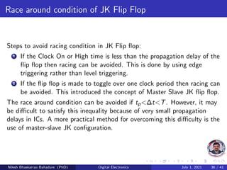
  • 138. Race around condition of JK Flip Flop Steps to avoid racing condition in JK Flip flop: 1 If the Clock On or High time is less than the propagation delay of the flip flop then racing can be avoided. This is done by using edge triggering rather than level triggering. Nilesh Bhaskarrao Bahadure (PhD) Digital Electronics July 1, 2021 36 / 41
  • 139. Race around condition of JK Flip Flop Steps to avoid racing condition in JK Flip flop: 1 If the Clock On or High time is less than the propagation delay of the flip flop then racing can be avoided. This is done by using edge triggering rather than level triggering. 2 If the flip flop is made to toggle over one clock period then racing can be avoided. This introduced the concept of Master Slave JK flip flop. Nilesh Bhaskarrao Bahadure (PhD) Digital Electronics July 1, 2021 36 / 41
  • 140. Race around condition of JK Flip Flop Steps to avoid racing condition in JK Flip flop: 1 If the Clock On or High time is less than the propagation delay of the flip flop then racing can be avoided. This is done by using edge triggering rather than level triggering. 2 If the flip flop is made to toggle over one clock period then racing can be avoided. This introduced the concept of Master Slave JK flip flop. Nilesh Bhaskarrao Bahadure (PhD) Digital Electronics July 1, 2021 36 / 41
  • 141. Race around condition of JK Flip Flop Steps to avoid racing condition in JK Flip flop: 1 If the Clock On or High time is less than the propagation delay of the flip flop then racing can be avoided. This is done by using edge triggering rather than level triggering. 2 If the flip flop is made to toggle over one clock period then racing can be avoided. This introduced the concept of Master Slave JK flip flop. The race around condition can be avoided if tp<∆t<T. However, it may be difficult to satisfy this inequality because of very small propagation delays in ICs. A more practical method for overcoming this difficulty is the use of master-slave JK configuration. Nilesh Bhaskarrao Bahadure (PhD) Digital Electronics July 1, 2021 36 / 41
  • 142. Master Slave JK Flip flop Nilesh Bhaskarrao Bahadure (PhD) Digital Electronics July 1, 2021 37 / 41
  • 143. Master Slave JK Flip flop The Master-Slave Flip-Flop is basically a combination of two JK flip-flops connected together in a series configuration. Out of these, one acts as the ”master” and the other as a ”slave”. The output from the master flip flop is connected to the two inputs of the slave flip flop whose output is fed back to inputs of the master flip flop. Nilesh Bhaskarrao Bahadure (PhD) Digital Electronics July 1, 2021 37 / 41
  • 144. Master Slave JK Flip flop The Master-Slave Flip-Flop is basically a combination of two JK flip-flops connected together in a series configuration. Out of these, one acts as the ”master” and the other as a ”slave”. The output from the master flip flop is connected to the two inputs of the slave flip flop whose output is fed back to inputs of the master flip flop. In addition to these two flip-flops, the circuit also includes an inverter. The inverter is connected to clock pulse in such a way that the inverted clock pulse is given to the slave flip-flop. In other words if CP=0 for a master flip-flop, then CP=1 for a slave flip-flop and if CP=1 for master flip flop then it becomes 0 for slave flip flop. Nilesh Bhaskarrao Bahadure (PhD) Digital Electronics July 1, 2021 37 / 41
  • 145. Master Slave JK Flip flop Nilesh Bhaskarrao Bahadure (PhD) Digital Electronics July 1, 2021 38 / 41
  • 146. Master Slave JK Flip flop Figure : master slave JK flip flop Nilesh Bhaskarrao Bahadure (PhD) Digital Electronics July 1, 2021 38 / 41
  • 147. Master Slave JK Flip flop Nilesh Bhaskarrao Bahadure (PhD) Digital Electronics July 1, 2021 39 / 41
  • 148. Master Slave JK Flip flop Figure : Circuit diagram of master slave JK flip flop Nilesh Bhaskarrao Bahadure (PhD) Digital Electronics July 1, 2021 39 / 41
  • 149. Working of a master slave flip flop 1 When the clock pulse goes to 1, the slave is isolated; J and K inputs may affect the state of the system. The slave flip-flop is isolated until the CP goes to 0. When the CP goes back to 0, information is passed from the master flip-flop to the slave and output is obtained. Nilesh Bhaskarrao Bahadure (PhD) Digital Electronics July 1, 2021 40 / 41
  • 150. Working of a master slave flip flop 1 When the clock pulse goes to 1, the slave is isolated; J and K inputs may affect the state of the system. The slave flip-flop is isolated until the CP goes to 0. When the CP goes back to 0, information is passed from the master flip-flop to the slave and output is obtained. 2 Firstly the master flip flop is positive level triggered and the slave flip flop is negative level triggered, so the master responds before the slave. Nilesh Bhaskarrao Bahadure (PhD) Digital Electronics July 1, 2021 40 / 41
  • 151. Working of a master slave flip flop 1 When the clock pulse goes to 1, the slave is isolated; J and K inputs may affect the state of the system. The slave flip-flop is isolated until the CP goes to 0. When the CP goes back to 0, information is passed from the master flip-flop to the slave and output is obtained. 2 Firstly the master flip flop is positive level triggered and the slave flip flop is negative level triggered, so the master responds before the slave. 3 If J=0 and K=1, the high Q’ output of the master goes to the K input of the slave and the clock forces the slave to reset, thus the slave copies the master. Nilesh Bhaskarrao Bahadure (PhD) Digital Electronics July 1, 2021 40 / 41
  • 152. Working of a master slave flip flop 1 When the clock pulse goes to 1, the slave is isolated; J and K inputs may affect the state of the system. The slave flip-flop is isolated until the CP goes to 0. When the CP goes back to 0, information is passed from the master flip-flop to the slave and output is obtained. 2 Firstly the master flip flop is positive level triggered and the slave flip flop is negative level triggered, so the master responds before the slave. 3 If J=0 and K=1, the high Q’ output of the master goes to the K input of the slave and the clock forces the slave to reset, thus the slave copies the master. 4 If J=1 and K=0, the high Q output of the master goes to the J input of the slave and the Negative transition of the clock sets the slave, copying the master. Nilesh Bhaskarrao Bahadure (PhD) Digital Electronics July 1, 2021 40 / 41
  • 153. Working of a master slave flip flop 1 When the clock pulse goes to 1, the slave is isolated; J and K inputs may affect the state of the system. The slave flip-flop is isolated until the CP goes to 0. When the CP goes back to 0, information is passed from the master flip-flop to the slave and output is obtained. 2 Firstly the master flip flop is positive level triggered and the slave flip flop is negative level triggered, so the master responds before the slave. 3 If J=0 and K=1, the high Q’ output of the master goes to the K input of the slave and the clock forces the slave to reset, thus the slave copies the master. 4 If J=1 and K=0, the high Q output of the master goes to the J input of the slave and the Negative transition of the clock sets the slave, copying the master. 5 If J=1 and K=1, it toggles on the positive transition of the clock and thus the slave toggles on the negative transition of the clock. Nilesh Bhaskarrao Bahadure (PhD) Digital Electronics July 1, 2021 40 / 41
  • 154. Working of a master slave flip flop 1 When the clock pulse goes to 1, the slave is isolated; J and K inputs may affect the state of the system. The slave flip-flop is isolated until the CP goes to 0. When the CP goes back to 0, information is passed from the master flip-flop to the slave and output is obtained. 2 Firstly the master flip flop is positive level triggered and the slave flip flop is negative level triggered, so the master responds before the slave. 3 If J=0 and K=1, the high Q’ output of the master goes to the K input of the slave and the clock forces the slave to reset, thus the slave copies the master. 4 If J=1 and K=0, the high Q output of the master goes to the J input of the slave and the Negative transition of the clock sets the slave, copying the master. 5 If J=1 and K=1, it toggles on the positive transition of the clock and thus the slave toggles on the negative transition of the clock. 6 If J=0 and K=0, the flip flop is disabled and Q remains unchanged. Nilesh Bhaskarrao Bahadure (PhD) Digital Electronics July 1, 2021 40 / 41
  • 155. Thank you Please send your feedback at nbahadure@gmail.com Nilesh Bhaskarrao Bahadure (PhD) Digital Electronics July 1, 2021 41 / 41
  • 156. Thank you Please send your feedback at nbahadure@gmail.com For download and more information Click Here Nilesh Bhaskarrao Bahadure (PhD) Digital Electronics July 1, 2021 41 / 41