SlideShare a Scribd company logo
 Unit 1: Introduction to 80386
 Unit 2: Bus Cycles and System Architecture
Microprocessor
1
2
Initialization
3
Initialization
4
• After a signal on the RESET pin, certain registers of 80386 are
set to predefined values.
• These values are adequate to enable execution of a bootstrap
program.
Processor State after RESET
• Contents of EAX depends on results power-up self test
• Self-test may be requested externally by assertion of BUSY# at the end of
RESET (EAX=0 if the 80386 passed the test, else 80386 unit is faulty)
• If self-test is not requested , EAX is undefined
• DX holds a component identifier and revision number
(DH=3, indicates 80386, DL=unique identifier of the revision level)
5
Introduction to Processor State
After Reset
6
• The 386 DX Microprocessorr has an input, called RESET# pin,
which invokes reset initialization.
• After asserting the signal on the RESET# Pin, some registers of
the 386 DX Microprocessor are set to known states.
• These known states,such as the contents of the EIP
register,are sufficient to allow software to begin execution.
• Software then can build the data structure in memory such as
the GDT and LDT tables, which are used by system and
application software.
• The 386 DX Microprocesssor has several processing modes.
Processor State After Reset with
RESET Signal
7
• Hardware assert the RESET# signal at powerup.
• Hardware may assert this signal at other times.for
example,a button may be provided for manually
invoking reset initialization.
• Reset also may be the response of Hardware to
receiving a halt or shutdown indication.
Self Test at Power-Up
8
• A self- Test may be requested at power up, a self test
is requested by asserting the signal on the BUSY# pin
during the falling edge of the RESET# Signal.
• RESET initialization take 350 to 450 clock periods
• If the self test is selected , it takes about 220
clock
periods
Contents of EAX Regiter.
9
• The contents of EAX depend upon the results of the
power-up self test.
• The EAX register is clear (holds zero)if the 386 DX
microprocessor passed the test.
• A non-zero value in the EAX register after self-test
indicates the processor is faulty.
• If the self-test is not requested, the contents of the
EAXregister after reset initialization are
undefined(possibly non-zero).
Contents of DX Register.
10
• The DX register holds a component identifier and revision number after reset
initialization, as shown in Figure.
• The DH register contains the value 3, which indicates a 386 DXmicroprocessor.
The DL register contains a unique identifier ofthe revision level.
The State of CR0 Register
• Control Register 0 (CR0) contains, The state of the CRO register following power-
up is shown in Figure. These states put the processor into real-address mode with
paging disabled.
11
State of flags and other registers
12
• The state of the EBX, ECX, ESI, EDI, EBP, ESP, GDTR, LDTR, TR and debug registers
is undefined following power-up.Software should not depend on any undefined states.
• The state of the flags and other registers following power-up isshown in Table
Activity After Reset
13
0
Software Initialization for real
Address Mode(Introduction)
• After reset initialization, software sets up data structures needed for
the processor to perform basic system functions, such as handling
interrupts.
• If the processor remains in real-address mode, software sets up data
structures in the form used by the 8086processor
• .If the processor is going to operate in protected mode software sets
up data structures in the form used by the80286 and 386 DX
microprocessors, then switches modes.
Software Initialization for real
Address Mode(STACK)
• No Instruction that use the stack can be used until the stack-
segment register(SS) has been loaded.
• SS must point to an area in RAM
Interrupt Table
• The initial state of the 80386 leaves interrupts disabled; however, the processor will still
attempt to access the interrupt table if an exception or non-maskable interrupt (NMI) occurs.
Initialization software should take one of the following actions:
• Change the limit value in the IDTR to zero. This will cause a shutdown if an exception or non-
maskable interrupt occurs.
• Put pointers to valid interrupt handlers in all positions of the interrupt table that might be
used by exceptions or interrupts.
• Change the IDTR to point to a valid interrupt table.
Address For First Instruction
• The CS register has two parts: the visible segment selector part and the hidden base address
part.
• In real-address mode, the base address is normally formed by shifting the 16-bit segment
selector value 4 bits to the left to produce a 20-bit base address.
• However, during a hardware reset, the segment selector in the CS register is loaded with
F000H and 20 bit base address is FOOOOH and the high 12 bits of addresses issued for the
code segment are set hence the 32 bit base address is FFFF0000H. The starting address is
thus formed by adding the base address to the value in the EIP register (FFFOH)
• (FFFF0000 + FFFOH = FFFFFFFOH).
• The first instruction that is fetched and executed following a hardware reset is located at
physical address FFFFFFFOH
First Instruction
• After RESET, address lines A{31-20} are automatically asserted for instruction fetches.
• This fact, together with the initial values of CS:IP, causes instruction execution to begin at
physical address FFFFFFFOH Near (intra segment) forms of control transfer instructions
maybe used to pass control to other addresses in the upper 64Kbytes of the address space.
• The first far (intersegment) JMP or CALL instruction causes A{31-20} to drop low, and the
80386 continues executing instructions in the lower one megabyte of physical memory.
• This automatic assertion of address lines A{31-20} allows systems designers to use a ROM
at the high end of the address space to initialize the system.
Micrprocessor unit 2 ppt This unit synchronizes all the microprocessor operations with the clock and generates the control signal necessary for communication between the microprocessor ...
Functional Pin Diagram
21
BUS CYCLE DEFINATION
M/IO# D/C# W/R# Type of Bus cycle
0 0 0 Interrupt Acknowledge
0 0 1 Bus Idle
0 1 0 I/O data read
0 1 1 I/O data write
1 0 0 Halt/Shutdown
1 1 0 Memory Data Read
1 1 1 Memory data wite
Decimal Address Binary Address (A31 to A0) A1 (Bit 1) A0 (Bit 0)
0 0000 0000 0000 0000 0000 0000 0000 0000 0 0
4 0000 0000 0000 0000 0000 0000 0000 0100 0 0
8 0000 0000 0000 0000 0000 0000 0000 1000 0
0
12 0000 0000 0000 0000 0000 0000 0000 1100 0 0
Pin Description Table
24
Pin Description Table (Cont…)
25
I/O Addressing
26
The 80386 allows input/output to be performed in either of two
ways:
a. By means of a separate I/O address space (using specific I/O
instructions)
b. By means of memory-mapped I/O (using
generalpurpose
operand manipulation instructions )
Some system designer may prefer to use the I/O Facilities built into
the processor, while others may prefer the simplicity of a single
physical address space.
I/O Addressing
27
Separate I/O Address Space Memory-Mapped I/O
Supported by special instruction The general purpose instruction set
can be used to access I/O Ports.
Supported by a hardware protection
mechanism.
Protection is provided using
segmentation or paging.
There is separate I/O Space I/O ports appears in the address space
of Physical Memory
Only IN and OUT instruction can access
such devices
e.g: IN AX, 45H
Any Memory related instruction will be
able to access this I/O device
e.g.: MOV BX, [3500H]
Separate I/O address space
(An Isolated I/O)
28
 I/O devices treated separately from memory.
• Hardware and software architecture of
8088/8086 support separate memory
I/O address space.
 Can be accessed as either byte-wide or word-wide.
 Can be treated as either independent byte-
wide I/O ports or word-wide I/O ports.
 Page 0:
• Certain I/O instructions can only perform
operations to ports in this part of the
address range.
• Other I/O instructions can input/output data
for ports anywhere in the address space.
Separate I/O address space
(An Isolated I/O)
29
Advantages: -
 1 MByte memory address space is available for use
with memory.
 Special instructions have been provided in the
instruction set of 8088/8086 to perform isolated
I/O input and output operations.
 These instructions have been tailored to maximize
I/O performance.
Disadvantages: -
 All input and output data transfers must take place
between AL or AX register and the I/O port
Memory-mapped I/O
I/O devices is placed in memory
address space of the
microcomputer.
• The memory address space
is assigned to I/O devices.
• MPU looks at the I/O port
as though it is a storage location
in memory.
• Make use of instructions that
affect data in memory rather than
special input/output instructions.
30
Memory-mapped I/O
Advantages:
 Many more instructions and addressing
modes are available to perform I/O
operations.
 I/O transfers can now take place
between I/O port and internal registers
other than just AL/AX.
Disadvantages:
 Memory instructions tend to execute
slower than those specifically designed
for isolated I/O.
 Part of the memory address space is
lost
31
I/O Instructions
32
There are two classes of I/O instruction:
1. Those that transfer a single item (byte, word, or doubleword)
located in a register.
2. Those that transfer strings of items (strings of bytes, words, or
doublewords) located in memory.
These are known as "string I/O instructions" or "block I/O
instructions".
Register I/O Instructions
• The I/O instructions IN and OUT
are provided to move
data between I/O ports and
the EAX (32-bit I/O), the
AX (I6-bit I/O), or AL (8-bit
I/O) general registers.
• IN and
addresses
OUT
instructions
I/O ports either
directly, with the address of one of
up to 256 port
33
Block I/O Instructions
34
• The block (or string) I/O instructions INS and OUTS move blocks of
data between I/O ports and memory space.
• Block I/O instructions use the DX register to specify the address of a
port in the I/O address space.
• Block I/O instructions use either SI or DI to designate the source or
destination memory address.
• For each transfer, SI or DI are automatically either incremented or
decremented as specified by the direction bit in the flags register.
Read and Write Cycles
35
• Data transfers occur as a result of bus cycles,
classified as read or write cycles.
• Two choices of address timing are
dynamically selectable: non-pipelined,
or
pipelined.
• After a bus idle state, the processor always
uses non-pipelined address timing.
• However, the NA# (Next Address) input may
be asserted to select pipelined
address timing for the next bus cycle.
• When pipelining is selected and the Intel386
DX has a bus request pending internally, the
address and definition of the next cycle is
made available even before the current bus
cycle is acknowledged by READY#.
• Terminating a read cycle or write cycle, like
any bus cycle, requires acknowledging the
cycle by asserting the READY# input.
• Until acknowledged, the processor inserts
wait states
Comparision B/W Non pipelined and Pipelined Bus
Cycle
Feature Non-Pipelined Bus Cycle Pipelined Bus Cycle
Address Strobe (ADS#) A new address is issued only after the previous cycle
completes.
New addresses are issued before the previous
cycle completes.
Bus Utilization Inefficient (idle gaps between cycles). Efficient (continuous data transfer, minimal idle
time).
Cycle Overlapping No overlapping of address and data phases. Overlapping of address and data phases to
improve performance.
NA# (Next Address Signal) Not used. Used to indicate that the bus is ready for the next
address.
Latency Higher, as each read/write must wait for the previous one
to finish.
Lower, as multiple transactions happen
simultaneously.
Performance Slower, as the bus is idle during certain phases. Faster, as the bus is always occupied with some
operation.
Wait States More likely to occur, as each cycle must fully complete
before the next starts.
Fewer wait states, since the processor can start a
new transaction while another is completing.
Complexity Simpler to implement. More complex due to overlapping cycles and the
need for NA# signal handling.
Use Case Used in simpler, slower systems where performance is not
critical.
Used in high-performance systems like 80386
and beyond to maximize efficiency.
Non-pipelined read & write cycles
37
Non-pipelined read cycles
38
Non-pipelined write cycles
39
pipelined write cycles
40
Non-pipelined read & write cycles
41
• At the end of the second bus state within the bus cycle,
READY# is sampled
• If asserted the bus cycle terminates
• Else the cycle continues another bus state (a wait state) and
READY# is sampled again at the end of that state.
• This continues indefinitely until the cycle is acknowledged by
READY# asserted.
System Architecture
42
Systems Architecture
43
Many of the architectural features of the 80386 are used only by systems programmers.This chapter
presents an overview of these aspects of the architecture.
• Memory Management
• Protection
• Multitasking
• Input/Output
• Exceptions and Interrupts
• Initialization.
• Coprocessing and Multiprocessing
• Debugging
These Features are implemented by registers and instructions
Systems Registers
44
• EFLAGS
• Memory Management Registers
• Control Registers
• Debug Registers
• Test Registers
Systems Registers
45
 EFLAGS
• Memory Management Registers
• Control Registers
• Debug Registers
• Test Registers
EFLAGS
System Flags of EFLAG REGISTER
46
Systems Flags
• The systems flags of the EFLAGS register control I/O, maskable interrupts,
debugging, task switching, and enabling of virtual 8086execution in a protected,
multitasking environment..
• IF (Interrupt-Enable Flag, bit 9) Setting IF allows the CPU to recognize
external (mask able) interrupt requests. Clearing IF disables these interrupts. IF
has no effect on either exceptions or non-maskable external interrupts..
• NT (Nested Task, bit 14) The processor uses the nested task flag to control
chaining of interrupted and called tasks. NT influences the operation of the
IRET instruction.
Systems Flags
• .RF (Resume Flag, bit 16) The RF flag temporarily disables debug exceptions so that
an instruction can be restarted after a debug exception without immediately causing
another debug exception.·
• TF (Trap Flag, bit 8) Setting TF puts the processor into single-step mode for
debugging. In this mode, the CPU automatically generates an exception after each
instruction, allowing a program to be inspected as it executes each instruction. Single-
stepping is just one of several debugging features of the 80386..
• VM (Virtual 8086 Mode, bit 17) When set, the VM flag indicates that the task is
executing an 8086 program. Refer to Chapter 14 for a detailed discussion of how the
80386 executes 8086 tasks in a protected, multitasking environment.
Systems Registers
49
• EFLAGS
 Memory Management Registers
• Control Registers
• Debug Registers
• Test Registers
Selector and Descriptor
The selector, located in the segment register, selects one of descriptors from one of two tables of
descriptors.
The descriptor (8 bytes), describes the location, length, and access rights of the segment of memory.
There are 2 descriptor tables:
1. Global descriptors: "system descriptor" contain segment definitions that apply to all programs
2. Local descriptors: "application descriptor" usually unique to an application.
• Each descriptor table contains 8192 descriptors. So total descriptors is 16,384, and the application
could have access to 4G X 16,384 = 64T bytes.
• In protected mode, this segment number can address any memory location in the system for the
code segment.
Memory-Management Registers
51
• Four registers of the 80386 locate the data structures that control segmented
memory management:
 GDTR Global Descriptor Table Register
 LDTR Local Descriptor Table Register
• These registers point to the segment descriptor tables GDT and LDT.
• IDTR Interrupt Descriptor Table Register
This register points to a table of entry points for interrupt handlers (the IDT).
• TR Task Register
This register points to the information needed by the processor to define the
current task.
Systems Registers
52
• EFLAGS
• Memory Management Registers
 Control Registers
• Debug Registers
• Test Registers
Control Registers
53
Systems Registers
54
• EFLAGS
• Memory Management Registers
• Control Registers
 Debug Registers
• Test Registers
Debug Registers
• Sixregisters: to control
debug features
• Accessed by variants of the MOV
instruction
• debug registers are
privileged resources
Registers are:
 Debug Address Registers (DRO-
DR3)
 Debug Status Register (DR6)
 Debug Control Register (DR7)
55
Introduction to Debug Registers
56
•Introduces six debug registers: DR0 - DR3, DR6, DR7.
•These are accessed using MOV instructions, but only at
privilege level 0.
•Attempting access at any other level results in a general
protection exception.
•Purpose: Debug registers help monitor instruction execution,
memory access, and control flow through hardware breakpoints.
Debug Address Registers(DR0-DR3)
57
• These registers store linear addresses for up to four
breakpoints.
• Work regardless of paging; if paging is enabled, the
CPU translates them to physical addresses.
• Used to set watchpoints to monitor:
• Instruction execution
• Memory reads or writes
• The type of monitoring is controlled by DR7.
Debug Control Registers(DR7)
(Configuring Breakpoints)
58
• .
•Purpose: Defines the behavior of breakpoints.
•Breakpoint conditions (R/W0 - R/W3):
•00: Break on instruction execution.
•01: Break on data writes.
•11: Break on data reads and writes (but not
instruction fetches).
•Length (LEN0 - LEN3): Specifies the size of data to
monitor.
•00: 1 byte
•01: 2 bytes
•11: 4 bytes
•Task-Switch Behavior:
•Local enable (L0-L3): Reset when tasks switch.
•Global enable (G0-G3): Remain active across
tasks.
•LE/GE Bits: Ensure precise breakpoint detection
by slowing execution.
Debug Status Register(DR6)
(Identifying Debug Event)
59
• Used to determine which debug condition triggered an exception.
• Flags:
• B0 - B3: Set if corresponding DR0-DR3 condition occurs.
• BT bit: Set if trap occurs during task switch due to T-bit in TSS.
• BS bit: Set if exception caused by single-step execution (TF bit in EFLAGS).
• BD bit: Set if an attempt is made to access debug registers while ICE-386 is using them.
• Handling DR6:
• CPU does not automatically clear DR6.
• Debug handler must manually clear DR6 before returning to avoid stale debug flags.
• .
Systems Registers
60
• EFLAGS
• Memory Management Registers
• Control Registers
• Debug Registers
 Test Registers
Test Registers
• Two test registers are provided for the purpose of testing.
• TR6 is the test command register, and TR7 is the test data
register.
• The test registers are privileged resources; in protected mode, the
MOV instructions that access them can only be executed at
privilege level 0
61
The Test Command Register (TR6)
• C: Command bit, two commands: ‘0’- write
entries into the TLB and ‘1’ perform
TLB lookups
• Linear Address(Tag Field serves as upper 20-bits
of linear address to be used for TLB Reference)
 on a TLB write command, a TLB entry is
allocated to this linear address and the rest of
that TLB entry is set as per the values of TR7 &
TR6
 on a TLB lookup command, the TLB is
interrogated as per this value and if one and
only one TLB entry matches, the rest of the
fields of TR6 & TR7 are set from the matching
TLB entry.
• V: The Valid bit for this TLB entry. The TLB uses the
valid bit to identify entries that contain valid data.
Entries of the TLB that have not been assigned values
have zero in the valid bit. All valid bits can be cleared
by writing to CR3.
• D, D#: The dirty bit for/from the TLB entry
• U, U#: The U/S bit for/from the TLB entry
• W, W#: The R/W bit for/from the TLB entry
Meaning of D, U, and W Bit Pairs
62
The Test Data Register (TR7)
63
Holds data read from or data to be written to the TLB
• Physical Address: This is the data field of the TLB. On a write to the TLB, the TLB
entry allocated to the linear address in TR6 is set to this value. On a TLB lookup,
if HT is set, the data field (physical address) from the TLB is read out to this field.
If HT is not set, this field is undefined.(This field contains either the physical
address to be written into TLB or the result of the valid TLB hit.)
• HT: For a TLB lookup, the HT bit indicates whether the lookup was a hit (HT <- 1)
or a miss (HT <- 0). For a TLB write, HT must be set to 1.
• REP: This is replacement pointer. This field indicates which set of the TLB four way
set associative catch to write to.
Test Operations
64
 To write a TLB entry
• Move a doubleword to TR7 that contains the desired physical address, HT, and
REP values. HT must contain 1. REP must point to the associative block in
which to place the entry
• Move a doubleword to TR6 that contains the appropriate linear address, and
values for V, D, U, and W. Be sure C=0 for "write" command.
 To look up (read) a TLB entry
• Move a doubleword to TR6 that contains the appropriate linear address and
attributes. Be sure C = 1 for "lookup" command
• Store TR 7. If the HT bit in TR 7 indicates a hit, then the other values reveal
the TLB contents. If HT indicates a miss, then the other values in TR 7 are
indeterminate
Systems Instructions
65
1. Verification of pointer parameters:
• ARPL ── Adjust RPL
• LAR ── Load Access Rights
• LSL ── Load Segment Limit
• VERR ── Verify for Reading
• VERW ── Verify for Writing
2. Addressing descriptor tables:
• LLDT ── Load LDT Register
• SLDT ── Store LDT Register
• LGDT ── Load GDT Register
• SGDT ── Store GDT Register
3. Multitasking:
• LTR ── Load Task Register
• STR ── Store Task Register
4. Coprocessing and Multiprocessing :
• CLTS ── Clear Task-Switched Flag
• ESC ── Escape instructions
• WAIT ── Wait until Coprocessor not
Busy
• LOCK ── Assert Bus-Lock Signal
Systems Instructions
66
5. Input and Output :
• IN ── Input
• OUT ── Output INS ── Input String
• OUTS ── Output String
6. Interrupt control :
• CLI ── Clear Interrupt-Enable Flag
• STI ── Set Interrupt-Enable Flag
• LIDT ── Load IDT Register
• SIDT ── Store IDT Register
9. System Control:
7. Debugging :
• MOV ── Move to and from debug
registers
8. TLB testing :
• MOV ── Move to and from test registers
• SMSW ── Set MSW
• LMSW ── Load MSW
• HLT ── Halt Processor
• MOV ── Move to and from control
registers
67
68

More Related Content

PDF
Introduction to 80386
PDF
VTU 4TH SEM CSE MICROPROCESSORS SOLVED PAPERS OF JUNE-2014 & JUNE-2015
PPTX
Pentium processor
PPT
The 80386 80486
PPT
Hafwgwhwhwhwhwwywwuwyeeeueue3UNIT 2 MP.ppt
PPTX
32- bit Microprocessor-Indtel 80386.pptx
PPT
8086_architecture MMC PPT.ppt
PPTX
8087_Coprocessorv1_1743590351714 (2).pptx
Introduction to 80386
VTU 4TH SEM CSE MICROPROCESSORS SOLVED PAPERS OF JUNE-2014 & JUNE-2015
Pentium processor
The 80386 80486
Hafwgwhwhwhwhwwywwuwyeeeueue3UNIT 2 MP.ppt
32- bit Microprocessor-Indtel 80386.pptx
8086_architecture MMC PPT.ppt
8087_Coprocessorv1_1743590351714 (2).pptx

Similar to Micrprocessor unit 2 ppt This unit synchronizes all the microprocessor operations with the clock and generates the control signal necessary for communication between the microprocessor ... (20)

PDF
80386_ Bus Cycles & System Architecture.pdf
PDF
Introduction to 80386 microprocessor
PPTX
8086 ppt
PPT
ADVANCED MICROPROCESSORS featuers, block diagram and register organization.ppt
PPTX
Computer Organization : CPU, Memory and I/O organization
PPTX
Microprocessors & Microcontrollers Architecture and Description
PDF
1 MPMC_8086 Architecture READ CAREFULLY.pdf
PPTX
CH-02 8086-microprocessor-architecture.pptx
DOC
the-cpu-design-central-processing-unit-design-1
PPTX
Pai unit 1_l1-l2-l3-l4_upload
PPTX
8086 microprocessor pptx JNTUH ece 3rd year
PDF
8086 Microprocessors and Microcontrollers
PDF
Microprocessors and microcontrollers
PPTX
UNIT 1.pptx
DOC
3 organization of intel 8086
PDF
2024_lecture6_come321.pdf...............................
PPT
8086_architecture.ppt
PPT
8086_architecture.ppt
PPT
8086_architecture.ppt
80386_ Bus Cycles & System Architecture.pdf
Introduction to 80386 microprocessor
8086 ppt
ADVANCED MICROPROCESSORS featuers, block diagram and register organization.ppt
Computer Organization : CPU, Memory and I/O organization
Microprocessors & Microcontrollers Architecture and Description
1 MPMC_8086 Architecture READ CAREFULLY.pdf
CH-02 8086-microprocessor-architecture.pptx
the-cpu-design-central-processing-unit-design-1
Pai unit 1_l1-l2-l3-l4_upload
8086 microprocessor pptx JNTUH ece 3rd year
8086 Microprocessors and Microcontrollers
Microprocessors and microcontrollers
UNIT 1.pptx
3 organization of intel 8086
2024_lecture6_come321.pdf...............................
8086_architecture.ppt
Ad

More from sayalishivarkar1 (10)

PPTX
IPR_Presentation_With_Design presenattion.pptx
PPTX
UNIT 2 PPT microprocessor presentation.pptx
PDF
seminar report kshitij on PBL presentation.pdf
PDF
Algo Strategies and explaination ppt.pdf
PPTX
unit-2-dsa.pptx
PPTX
DSA Unit II array.pptx
PPTX
FDS Unit I_PPT.pptx
PPTX
UNIT-II MMB.pptx
PDF
Unit 01 (1).pdf
PPTX
UNIT-I.pptx
IPR_Presentation_With_Design presenattion.pptx
UNIT 2 PPT microprocessor presentation.pptx
seminar report kshitij on PBL presentation.pdf
Algo Strategies and explaination ppt.pdf
unit-2-dsa.pptx
DSA Unit II array.pptx
FDS Unit I_PPT.pptx
UNIT-II MMB.pptx
Unit 01 (1).pdf
UNIT-I.pptx
Ad

Recently uploaded (20)

PPTX
Sustainable Sites - Green Building Construction
PPT
Project quality management in manufacturing
PPTX
UNIT 4 Total Quality Management .pptx
PDF
SM_6th-Sem__Cse_Internet-of-Things.pdf IOT
PDF
R24 SURVEYING LAB MANUAL for civil enggi
PPTX
bas. eng. economics group 4 presentation 1.pptx
PPTX
Construction Project Organization Group 2.pptx
PDF
Well-logging-methods_new................
PPTX
MET 305 2019 SCHEME MODULE 2 COMPLETE.pptx
PDF
Embodied AI: Ushering in the Next Era of Intelligent Systems
PPTX
UNIT-1 - COAL BASED THERMAL POWER PLANTS
PPTX
Internet of Things (IOT) - A guide to understanding
PPT
introduction to datamining and warehousing
PPTX
additive manufacturing of ss316l using mig welding
PDF
Automation-in-Manufacturing-Chapter-Introduction.pdf
PDF
The CXO Playbook 2025 – Future-Ready Strategies for C-Suite Leaders Cerebrai...
PPT
Mechanical Engineering MATERIALS Selection
PDF
Enhancing Cyber Defense Against Zero-Day Attacks using Ensemble Neural Networks
DOCX
ASol_English-Language-Literature-Set-1-27-02-2023-converted.docx
PPTX
Safety Seminar civil to be ensured for safe working.
Sustainable Sites - Green Building Construction
Project quality management in manufacturing
UNIT 4 Total Quality Management .pptx
SM_6th-Sem__Cse_Internet-of-Things.pdf IOT
R24 SURVEYING LAB MANUAL for civil enggi
bas. eng. economics group 4 presentation 1.pptx
Construction Project Organization Group 2.pptx
Well-logging-methods_new................
MET 305 2019 SCHEME MODULE 2 COMPLETE.pptx
Embodied AI: Ushering in the Next Era of Intelligent Systems
UNIT-1 - COAL BASED THERMAL POWER PLANTS
Internet of Things (IOT) - A guide to understanding
introduction to datamining and warehousing
additive manufacturing of ss316l using mig welding
Automation-in-Manufacturing-Chapter-Introduction.pdf
The CXO Playbook 2025 – Future-Ready Strategies for C-Suite Leaders Cerebrai...
Mechanical Engineering MATERIALS Selection
Enhancing Cyber Defense Against Zero-Day Attacks using Ensemble Neural Networks
ASol_English-Language-Literature-Set-1-27-02-2023-converted.docx
Safety Seminar civil to be ensured for safe working.

Micrprocessor unit 2 ppt This unit synchronizes all the microprocessor operations with the clock and generates the control signal necessary for communication between the microprocessor ...

  • 1.  Unit 1: Introduction to 80386  Unit 2: Bus Cycles and System Architecture Microprocessor 1
  • 2. 2
  • 4. Initialization 4 • After a signal on the RESET pin, certain registers of 80386 are set to predefined values. • These values are adequate to enable execution of a bootstrap program.
  • 5. Processor State after RESET • Contents of EAX depends on results power-up self test • Self-test may be requested externally by assertion of BUSY# at the end of RESET (EAX=0 if the 80386 passed the test, else 80386 unit is faulty) • If self-test is not requested , EAX is undefined • DX holds a component identifier and revision number (DH=3, indicates 80386, DL=unique identifier of the revision level) 5
  • 6. Introduction to Processor State After Reset 6 • The 386 DX Microprocessorr has an input, called RESET# pin, which invokes reset initialization. • After asserting the signal on the RESET# Pin, some registers of the 386 DX Microprocessor are set to known states. • These known states,such as the contents of the EIP register,are sufficient to allow software to begin execution. • Software then can build the data structure in memory such as the GDT and LDT tables, which are used by system and application software. • The 386 DX Microprocesssor has several processing modes.
  • 7. Processor State After Reset with RESET Signal 7 • Hardware assert the RESET# signal at powerup. • Hardware may assert this signal at other times.for example,a button may be provided for manually invoking reset initialization. • Reset also may be the response of Hardware to receiving a halt or shutdown indication.
  • 8. Self Test at Power-Up 8 • A self- Test may be requested at power up, a self test is requested by asserting the signal on the BUSY# pin during the falling edge of the RESET# Signal. • RESET initialization take 350 to 450 clock periods • If the self test is selected , it takes about 220 clock periods
  • 9. Contents of EAX Regiter. 9 • The contents of EAX depend upon the results of the power-up self test. • The EAX register is clear (holds zero)if the 386 DX microprocessor passed the test. • A non-zero value in the EAX register after self-test indicates the processor is faulty. • If the self-test is not requested, the contents of the EAXregister after reset initialization are undefined(possibly non-zero).
  • 10. Contents of DX Register. 10 • The DX register holds a component identifier and revision number after reset initialization, as shown in Figure. • The DH register contains the value 3, which indicates a 386 DXmicroprocessor. The DL register contains a unique identifier ofthe revision level.
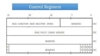
  • 11. The State of CR0 Register • Control Register 0 (CR0) contains, The state of the CRO register following power- up is shown in Figure. These states put the processor into real-address mode with paging disabled. 11
  • 12. State of flags and other registers 12 • The state of the EBX, ECX, ESI, EDI, EBP, ESP, GDTR, LDTR, TR and debug registers is undefined following power-up.Software should not depend on any undefined states. • The state of the flags and other registers following power-up isshown in Table
  • 14. Software Initialization for real Address Mode(Introduction) • After reset initialization, software sets up data structures needed for the processor to perform basic system functions, such as handling interrupts. • If the processor remains in real-address mode, software sets up data structures in the form used by the 8086processor • .If the processor is going to operate in protected mode software sets up data structures in the form used by the80286 and 386 DX microprocessors, then switches modes.
  • 15. Software Initialization for real Address Mode(STACK) • No Instruction that use the stack can be used until the stack- segment register(SS) has been loaded. • SS must point to an area in RAM
  • 16. Interrupt Table • The initial state of the 80386 leaves interrupts disabled; however, the processor will still attempt to access the interrupt table if an exception or non-maskable interrupt (NMI) occurs. Initialization software should take one of the following actions: • Change the limit value in the IDTR to zero. This will cause a shutdown if an exception or non- maskable interrupt occurs. • Put pointers to valid interrupt handlers in all positions of the interrupt table that might be used by exceptions or interrupts. • Change the IDTR to point to a valid interrupt table.
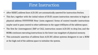
  • 17. Address For First Instruction • The CS register has two parts: the visible segment selector part and the hidden base address part. • In real-address mode, the base address is normally formed by shifting the 16-bit segment selector value 4 bits to the left to produce a 20-bit base address. • However, during a hardware reset, the segment selector in the CS register is loaded with F000H and 20 bit base address is FOOOOH and the high 12 bits of addresses issued for the code segment are set hence the 32 bit base address is FFFF0000H. The starting address is thus formed by adding the base address to the value in the EIP register (FFFOH) • (FFFF0000 + FFFOH = FFFFFFFOH). • The first instruction that is fetched and executed following a hardware reset is located at physical address FFFFFFFOH
  • 18. First Instruction • After RESET, address lines A{31-20} are automatically asserted for instruction fetches. • This fact, together with the initial values of CS:IP, causes instruction execution to begin at physical address FFFFFFFOH Near (intra segment) forms of control transfer instructions maybe used to pass control to other addresses in the upper 64Kbytes of the address space. • The first far (intersegment) JMP or CALL instruction causes A{31-20} to drop low, and the 80386 continues executing instructions in the lower one megabyte of physical memory. • This automatic assertion of address lines A{31-20} allows systems designers to use a ROM at the high end of the address space to initialize the system.
  • 22. BUS CYCLE DEFINATION M/IO# D/C# W/R# Type of Bus cycle 0 0 0 Interrupt Acknowledge 0 0 1 Bus Idle 0 1 0 I/O data read 0 1 1 I/O data write 1 0 0 Halt/Shutdown 1 1 0 Memory Data Read 1 1 1 Memory data wite
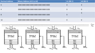
  • 23. Decimal Address Binary Address (A31 to A0) A1 (Bit 1) A0 (Bit 0) 0 0000 0000 0000 0000 0000 0000 0000 0000 0 0 4 0000 0000 0000 0000 0000 0000 0000 0100 0 0 8 0000 0000 0000 0000 0000 0000 0000 1000 0 0 12 0000 0000 0000 0000 0000 0000 0000 1100 0 0
  • 25. Pin Description Table (Cont…) 25
  • 26. I/O Addressing 26 The 80386 allows input/output to be performed in either of two ways: a. By means of a separate I/O address space (using specific I/O instructions) b. By means of memory-mapped I/O (using generalpurpose operand manipulation instructions ) Some system designer may prefer to use the I/O Facilities built into the processor, while others may prefer the simplicity of a single physical address space.
  • 27. I/O Addressing 27 Separate I/O Address Space Memory-Mapped I/O Supported by special instruction The general purpose instruction set can be used to access I/O Ports. Supported by a hardware protection mechanism. Protection is provided using segmentation or paging. There is separate I/O Space I/O ports appears in the address space of Physical Memory Only IN and OUT instruction can access such devices e.g: IN AX, 45H Any Memory related instruction will be able to access this I/O device e.g.: MOV BX, [3500H]
  • 28. Separate I/O address space (An Isolated I/O) 28  I/O devices treated separately from memory. • Hardware and software architecture of 8088/8086 support separate memory I/O address space.  Can be accessed as either byte-wide or word-wide.  Can be treated as either independent byte- wide I/O ports or word-wide I/O ports.  Page 0: • Certain I/O instructions can only perform operations to ports in this part of the address range. • Other I/O instructions can input/output data for ports anywhere in the address space.
  • 29. Separate I/O address space (An Isolated I/O) 29 Advantages: -  1 MByte memory address space is available for use with memory.  Special instructions have been provided in the instruction set of 8088/8086 to perform isolated I/O input and output operations.  These instructions have been tailored to maximize I/O performance. Disadvantages: -  All input and output data transfers must take place between AL or AX register and the I/O port
  • 30. Memory-mapped I/O I/O devices is placed in memory address space of the microcomputer. • The memory address space is assigned to I/O devices. • MPU looks at the I/O port as though it is a storage location in memory. • Make use of instructions that affect data in memory rather than special input/output instructions. 30
  • 31. Memory-mapped I/O Advantages:  Many more instructions and addressing modes are available to perform I/O operations.  I/O transfers can now take place between I/O port and internal registers other than just AL/AX. Disadvantages:  Memory instructions tend to execute slower than those specifically designed for isolated I/O.  Part of the memory address space is lost 31
  • 32. I/O Instructions 32 There are two classes of I/O instruction: 1. Those that transfer a single item (byte, word, or doubleword) located in a register. 2. Those that transfer strings of items (strings of bytes, words, or doublewords) located in memory. These are known as "string I/O instructions" or "block I/O instructions".
  • 33. Register I/O Instructions • The I/O instructions IN and OUT are provided to move data between I/O ports and the EAX (32-bit I/O), the AX (I6-bit I/O), or AL (8-bit I/O) general registers. • IN and addresses OUT instructions I/O ports either directly, with the address of one of up to 256 port 33
  • 34. Block I/O Instructions 34 • The block (or string) I/O instructions INS and OUTS move blocks of data between I/O ports and memory space. • Block I/O instructions use the DX register to specify the address of a port in the I/O address space. • Block I/O instructions use either SI or DI to designate the source or destination memory address. • For each transfer, SI or DI are automatically either incremented or decremented as specified by the direction bit in the flags register.
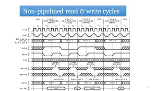
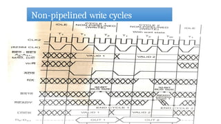
  • 35. Read and Write Cycles 35 • Data transfers occur as a result of bus cycles, classified as read or write cycles. • Two choices of address timing are dynamically selectable: non-pipelined, or pipelined. • After a bus idle state, the processor always uses non-pipelined address timing. • However, the NA# (Next Address) input may be asserted to select pipelined address timing for the next bus cycle. • When pipelining is selected and the Intel386 DX has a bus request pending internally, the address and definition of the next cycle is made available even before the current bus cycle is acknowledged by READY#. • Terminating a read cycle or write cycle, like any bus cycle, requires acknowledging the cycle by asserting the READY# input. • Until acknowledged, the processor inserts wait states
  • 36. Comparision B/W Non pipelined and Pipelined Bus Cycle Feature Non-Pipelined Bus Cycle Pipelined Bus Cycle Address Strobe (ADS#) A new address is issued only after the previous cycle completes. New addresses are issued before the previous cycle completes. Bus Utilization Inefficient (idle gaps between cycles). Efficient (continuous data transfer, minimal idle time). Cycle Overlapping No overlapping of address and data phases. Overlapping of address and data phases to improve performance. NA# (Next Address Signal) Not used. Used to indicate that the bus is ready for the next address. Latency Higher, as each read/write must wait for the previous one to finish. Lower, as multiple transactions happen simultaneously. Performance Slower, as the bus is idle during certain phases. Faster, as the bus is always occupied with some operation. Wait States More likely to occur, as each cycle must fully complete before the next starts. Fewer wait states, since the processor can start a new transaction while another is completing. Complexity Simpler to implement. More complex due to overlapping cycles and the need for NA# signal handling. Use Case Used in simpler, slower systems where performance is not critical. Used in high-performance systems like 80386 and beyond to maximize efficiency.
  • 37. Non-pipelined read & write cycles 37
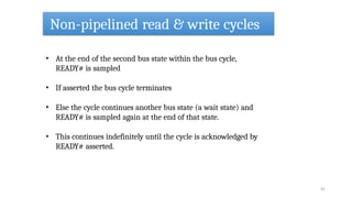
  • 41. Non-pipelined read & write cycles 41 • At the end of the second bus state within the bus cycle, READY# is sampled • If asserted the bus cycle terminates • Else the cycle continues another bus state (a wait state) and READY# is sampled again at the end of that state. • This continues indefinitely until the cycle is acknowledged by READY# asserted.
  • 43. Systems Architecture 43 Many of the architectural features of the 80386 are used only by systems programmers.This chapter presents an overview of these aspects of the architecture. • Memory Management • Protection • Multitasking • Input/Output • Exceptions and Interrupts • Initialization. • Coprocessing and Multiprocessing • Debugging These Features are implemented by registers and instructions
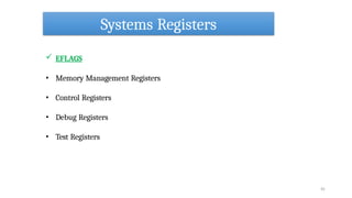
  • 44. Systems Registers 44 • EFLAGS • Memory Management Registers • Control Registers • Debug Registers • Test Registers
  • 45. Systems Registers 45  EFLAGS • Memory Management Registers • Control Registers • Debug Registers • Test Registers
  • 46. EFLAGS System Flags of EFLAG REGISTER 46
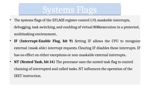
  • 47. Systems Flags • The systems flags of the EFLAGS register control I/O, maskable interrupts, debugging, task switching, and enabling of virtual 8086execution in a protected, multitasking environment.. • IF (Interrupt-Enable Flag, bit 9) Setting IF allows the CPU to recognize external (mask able) interrupt requests. Clearing IF disables these interrupts. IF has no effect on either exceptions or non-maskable external interrupts.. • NT (Nested Task, bit 14) The processor uses the nested task flag to control chaining of interrupted and called tasks. NT influences the operation of the IRET instruction.
  • 48. Systems Flags • .RF (Resume Flag, bit 16) The RF flag temporarily disables debug exceptions so that an instruction can be restarted after a debug exception without immediately causing another debug exception.· • TF (Trap Flag, bit 8) Setting TF puts the processor into single-step mode for debugging. In this mode, the CPU automatically generates an exception after each instruction, allowing a program to be inspected as it executes each instruction. Single- stepping is just one of several debugging features of the 80386.. • VM (Virtual 8086 Mode, bit 17) When set, the VM flag indicates that the task is executing an 8086 program. Refer to Chapter 14 for a detailed discussion of how the 80386 executes 8086 tasks in a protected, multitasking environment.
  • 49. Systems Registers 49 • EFLAGS  Memory Management Registers • Control Registers • Debug Registers • Test Registers
  • 50. Selector and Descriptor The selector, located in the segment register, selects one of descriptors from one of two tables of descriptors. The descriptor (8 bytes), describes the location, length, and access rights of the segment of memory. There are 2 descriptor tables: 1. Global descriptors: "system descriptor" contain segment definitions that apply to all programs 2. Local descriptors: "application descriptor" usually unique to an application. • Each descriptor table contains 8192 descriptors. So total descriptors is 16,384, and the application could have access to 4G X 16,384 = 64T bytes. • In protected mode, this segment number can address any memory location in the system for the code segment.
  • 51. Memory-Management Registers 51 • Four registers of the 80386 locate the data structures that control segmented memory management:  GDTR Global Descriptor Table Register  LDTR Local Descriptor Table Register • These registers point to the segment descriptor tables GDT and LDT. • IDTR Interrupt Descriptor Table Register This register points to a table of entry points for interrupt handlers (the IDT). • TR Task Register This register points to the information needed by the processor to define the current task.
  • 52. Systems Registers 52 • EFLAGS • Memory Management Registers  Control Registers • Debug Registers • Test Registers
  • 54. Systems Registers 54 • EFLAGS • Memory Management Registers • Control Registers  Debug Registers • Test Registers
  • 55. Debug Registers • Sixregisters: to control debug features • Accessed by variants of the MOV instruction • debug registers are privileged resources Registers are:  Debug Address Registers (DRO- DR3)  Debug Status Register (DR6)  Debug Control Register (DR7) 55
  • 56. Introduction to Debug Registers 56 •Introduces six debug registers: DR0 - DR3, DR6, DR7. •These are accessed using MOV instructions, but only at privilege level 0. •Attempting access at any other level results in a general protection exception. •Purpose: Debug registers help monitor instruction execution, memory access, and control flow through hardware breakpoints.
  • 57. Debug Address Registers(DR0-DR3) 57 • These registers store linear addresses for up to four breakpoints. • Work regardless of paging; if paging is enabled, the CPU translates them to physical addresses. • Used to set watchpoints to monitor: • Instruction execution • Memory reads or writes • The type of monitoring is controlled by DR7.
  • 58. Debug Control Registers(DR7) (Configuring Breakpoints) 58 • . •Purpose: Defines the behavior of breakpoints. •Breakpoint conditions (R/W0 - R/W3): •00: Break on instruction execution. •01: Break on data writes. •11: Break on data reads and writes (but not instruction fetches). •Length (LEN0 - LEN3): Specifies the size of data to monitor. •00: 1 byte •01: 2 bytes •11: 4 bytes •Task-Switch Behavior: •Local enable (L0-L3): Reset when tasks switch. •Global enable (G0-G3): Remain active across tasks. •LE/GE Bits: Ensure precise breakpoint detection by slowing execution.
  • 59. Debug Status Register(DR6) (Identifying Debug Event) 59 • Used to determine which debug condition triggered an exception. • Flags: • B0 - B3: Set if corresponding DR0-DR3 condition occurs. • BT bit: Set if trap occurs during task switch due to T-bit in TSS. • BS bit: Set if exception caused by single-step execution (TF bit in EFLAGS). • BD bit: Set if an attempt is made to access debug registers while ICE-386 is using them. • Handling DR6: • CPU does not automatically clear DR6. • Debug handler must manually clear DR6 before returning to avoid stale debug flags. • .
  • 60. Systems Registers 60 • EFLAGS • Memory Management Registers • Control Registers • Debug Registers  Test Registers
  • 61. Test Registers • Two test registers are provided for the purpose of testing. • TR6 is the test command register, and TR7 is the test data register. • The test registers are privileged resources; in protected mode, the MOV instructions that access them can only be executed at privilege level 0 61
  • 62. The Test Command Register (TR6) • C: Command bit, two commands: ‘0’- write entries into the TLB and ‘1’ perform TLB lookups • Linear Address(Tag Field serves as upper 20-bits of linear address to be used for TLB Reference)  on a TLB write command, a TLB entry is allocated to this linear address and the rest of that TLB entry is set as per the values of TR7 & TR6  on a TLB lookup command, the TLB is interrogated as per this value and if one and only one TLB entry matches, the rest of the fields of TR6 & TR7 are set from the matching TLB entry. • V: The Valid bit for this TLB entry. The TLB uses the valid bit to identify entries that contain valid data. Entries of the TLB that have not been assigned values have zero in the valid bit. All valid bits can be cleared by writing to CR3. • D, D#: The dirty bit for/from the TLB entry • U, U#: The U/S bit for/from the TLB entry • W, W#: The R/W bit for/from the TLB entry Meaning of D, U, and W Bit Pairs 62
  • 63. The Test Data Register (TR7) 63 Holds data read from or data to be written to the TLB • Physical Address: This is the data field of the TLB. On a write to the TLB, the TLB entry allocated to the linear address in TR6 is set to this value. On a TLB lookup, if HT is set, the data field (physical address) from the TLB is read out to this field. If HT is not set, this field is undefined.(This field contains either the physical address to be written into TLB or the result of the valid TLB hit.) • HT: For a TLB lookup, the HT bit indicates whether the lookup was a hit (HT <- 1) or a miss (HT <- 0). For a TLB write, HT must be set to 1. • REP: This is replacement pointer. This field indicates which set of the TLB four way set associative catch to write to.
  • 64. Test Operations 64  To write a TLB entry • Move a doubleword to TR7 that contains the desired physical address, HT, and REP values. HT must contain 1. REP must point to the associative block in which to place the entry • Move a doubleword to TR6 that contains the appropriate linear address, and values for V, D, U, and W. Be sure C=0 for "write" command.  To look up (read) a TLB entry • Move a doubleword to TR6 that contains the appropriate linear address and attributes. Be sure C = 1 for "lookup" command • Store TR 7. If the HT bit in TR 7 indicates a hit, then the other values reveal the TLB contents. If HT indicates a miss, then the other values in TR 7 are indeterminate
  • 65. Systems Instructions 65 1. Verification of pointer parameters: • ARPL ── Adjust RPL • LAR ── Load Access Rights • LSL ── Load Segment Limit • VERR ── Verify for Reading • VERW ── Verify for Writing 2. Addressing descriptor tables: • LLDT ── Load LDT Register • SLDT ── Store LDT Register • LGDT ── Load GDT Register • SGDT ── Store GDT Register 3. Multitasking: • LTR ── Load Task Register • STR ── Store Task Register 4. Coprocessing and Multiprocessing : • CLTS ── Clear Task-Switched Flag • ESC ── Escape instructions • WAIT ── Wait until Coprocessor not Busy • LOCK ── Assert Bus-Lock Signal
  • 66. Systems Instructions 66 5. Input and Output : • IN ── Input • OUT ── Output INS ── Input String • OUTS ── Output String 6. Interrupt control : • CLI ── Clear Interrupt-Enable Flag • STI ── Set Interrupt-Enable Flag • LIDT ── Load IDT Register • SIDT ── Store IDT Register 9. System Control: 7. Debugging : • MOV ── Move to and from debug registers 8. TLB testing : • MOV ── Move to and from test registers • SMSW ── Set MSW • LMSW ── Load MSW • HLT ── Halt Processor • MOV ── Move to and from control registers
  • 67. 67
  • 68. 68