SlideShare a Scribd company logo
DESIGN PROCEDURE
D.R.V.L.B Thambawita
October 29, 2017
D.R.V.L.B Thambawita DESIGN PROCEDURE
https://sites.google.com/view/vajira-thambawita/leaning-materials/slides
DESIGN PROCEDURE
Design procedures or methodologies specify hardware that will
implement a desired behavior.
The design effort for small circuits may be manual, but
industry relies on automated synthesis tools for designing
massive integrated circuits.
The design of a clocked sequential circuit starts from a set of
specifications and culminates in a logic diagram or a list
of Boolean functions from which the logic diagram can be
obtained.
In contrast to a combinational circuit, which is fully specified
by a truth table, a sequential circuit requires a state table for
its specification.
The first step in the design of sequential circuits is to obtain a
state table or an equivalent representation, such as a state
diagram.
D.R.V.L.B Thambawita DESIGN PROCEDURE
DESIGN PROCEDURE
1 From the word description and specifications of the desired
operation, derive a state diagram for the circuit.
2 Reduce the number of states if necessary.
3 Assign binary values to the states.
4 Obtain the binary-coded state table.
5 Choose the type of flip-flops to be used.
6 Derive the simplified flip-flop input equations and output
equations.
7 Draw the logic diagram.
D.R.V.L.B Thambawita DESIGN PROCEDURE
DESIGN PROCEDURE: Example
Suppose we wish to design a circuit that detects a sequence of
three or more consecutive 1’s in a string of bits coming through an
input line (the input is a serial bit stream).
D.R.V.L.B Thambawita DESIGN PROCEDURE
DESIGN PROCEDURE: Example
We need to assign binary codes to the states and list the state
table.
We choose two D flip-flops to represent the four states, and
we label their outputs A and B .
There is one input x and one output y.
D.R.V.L.B Thambawita DESIGN PROCEDURE
DESIGN PROCEDURE: Example
The characteristic equation of the D flip-flop is Q(t +1) = DQ
Which means that the next-state values in the state table
specify the D input condition for the flip-flop.
The flip-flop input equations can be obtained directly from
the next-state columns of A and B and expressed in
sum-of-minterms form as
A(t + 1) = DA(A, B, x) = (3, 5, 7)
B(t + 1) = DB(A, B, x) = (1, 5, 7)
y(A, B, x) = (6, 7)
D.R.V.L.B Thambawita DESIGN PROCEDURE
DESIGN PROCEDURE: Example
The Boolean equations are simplified by means of the maps
plotted in the following figure.
DA = Ax + Bx
DB = Ax + B x
y = AB
The advantage of designing withD flip-flops is that the Boolean
equations describing the inputs to the flip-flops can be obtained
directly from the state table.
D.R.V.L.B Thambawita DESIGN PROCEDURE
DESIGN PROCEDURE: Example
Figure: Moore type circuit
D.R.V.L.B Thambawita DESIGN PROCEDURE
Excitation Tables
When D -type flip-flops are employed, the input equations are
obtained directly from the next state.
This is not the case for the JK and T types of flip-flops.
It is necessary to derive a functional relationship between the
state table and the input equations.
The flip-flop characteristic tables are useful for analyzing
sequential circuits and for defining the operation of the
flip-flops.
During the design process, we usually know the transition
from the present state to the next state.
Wish to find the flip-flop input conditions that will cause the
required transition.
we need a table that lists the required inputs for a given
change of state. Such a table is called an excitation table .
D.R.V.L.B Thambawita DESIGN PROCEDURE
Excitation Tables
Do you remember?
Figure: Characteristic Tables
D.R.V.L.B Thambawita DESIGN PROCEDURE
Excitation Tables
Figure: Flip-Flop Excitation Tables
D.R.V.L.B Thambawita DESIGN PROCEDURE
Synthesis Using JK Flip-Flops
Example:
Figure: State Table and JK Flip-Flop Inputs
D.R.V.L.B Thambawita DESIGN PROCEDURE
Example:JK flip-flop
Figure: Maps for J and K input equations
D.R.V.L.B Thambawita DESIGN PROCEDURE
Example:JK flip-flop
Figure: Logic diagram for sequential circuit with JK flip-flops
D.R.V.L.B Thambawita DESIGN PROCEDURE
Synthesis Using T Flip-Flops
Figure: State diagram of three-bit binary counter
D.R.V.L.B Thambawita DESIGN PROCEDURE
Synthesis Using T Flip-Flops
Figure: State Table for Three-Bit Counter
D.R.V.L.B Thambawita DESIGN PROCEDURE
Synthesis Using T Flip-Flops
Figure: Maps for three-bit binary counter
D.R.V.L.B Thambawita DESIGN PROCEDURE
Synthesis Using T Flip-Flops
Figure: Logic diagram of three-bit binary counter
D.R.V.L.B Thambawita DESIGN PROCEDURE

More Related Content

PDF
Lec 07 - ANALYSIS OF CLOCKED SEQUENTIAL CIRCUITS
PPT
Sequential circuits
PDF
Combinational and sequential logic
PPTX
Generalized Isomorphism between Synchronous Circuits and State Machines
PDF
8085 arithmetic instructions
PDF
Modern Control System (BE)
PPT
State space analysis, eign values and eign vectors
PPTX
9. 8085 instruction set v
Lec 07 - ANALYSIS OF CLOCKED SEQUENTIAL CIRCUITS
Sequential circuits
Combinational and sequential logic
Generalized Isomorphism between Synchronous Circuits and State Machines
8085 arithmetic instructions
Modern Control System (BE)
State space analysis, eign values and eign vectors
9. 8085 instruction set v

What's hot (20)

PPSX
linear algebra in control systems
PDF
8085 data transfer instruction set
PDF
The Controller Design For Linear System: A State Space Approach
PPTX
Week 15 state space rep may 25 2016 final
PPT
Cd2 [autosaved]
PDF
TMPA-2017: Modeling of PLC-programs by High-level Coloured Petri Nets
PDF
Reduction of multiple subsystem [compatibility mode]
PPTX
Lecture 8-9 block-diagram_representation_of_control_systems
PDF
Block diagrams
PPTX
Instruction set
PPT
MICROPROCESSOR INSTRUCTION SET OF 8085
PPTX
State equations for physical systems
ODP
Program Derivation of Matrix Operations in GF
PDF
Introduction to Control systems in scilab
PPT
Design and minimization of reversible programmable logic arrays and its reali...
PPTX
block diagram representation of control systems
PPTX
Instruction set of 8085 microprocessor
PPTX
Block diagram
PPTX
Reversible logic gate
PPTX
Block diagram representation 3
linear algebra in control systems
8085 data transfer instruction set
The Controller Design For Linear System: A State Space Approach
Week 15 state space rep may 25 2016 final
Cd2 [autosaved]
TMPA-2017: Modeling of PLC-programs by High-level Coloured Petri Nets
Reduction of multiple subsystem [compatibility mode]
Lecture 8-9 block-diagram_representation_of_control_systems
Block diagrams
Instruction set
MICROPROCESSOR INSTRUCTION SET OF 8085
State equations for physical systems
Program Derivation of Matrix Operations in GF
Introduction to Control systems in scilab
Design and minimization of reversible programmable logic arrays and its reali...
block diagram representation of control systems
Instruction set of 8085 microprocessor
Block diagram
Reversible logic gate
Block diagram representation 3
Ad

Similar to Lec 08 - DESIGN PROCEDURE (20)

PPTX
Chapter-6-Synchronous Sequential Logic (2).pptx
PPT
Lec 25 26_27
PDF
Lecture0_Review_digkjital_design (1).pdf
PDF
Sequential Circuit
PPTX
Unit I_CDA-1 computer design and applications.
PPTX
PDF
DLD Lecture Unit 4 (1).pdf
PPTX
DD Slides6.pptx aaaaaaaaaaaaaaaaaaaaaaaaaaaa
PDF
DD lectures_17-09 to 24-09BITS2024-2025(1).pdf
PDF
Eceg 3201-dld-lec 12-synchronous_counter_design
PPTX
Sequential and combinational alu
PPT
Lec16 Intro to Computer Engineering by Hsien-Hsin Sean Lee Georgia Tech -- Fi...
DOCX
Gate Diffusion Input Technology (Very Large Scale Integration)
PDF
Counter design.pdf
PPTX
Flip flop’s state tables & diagrams
PDF
Analysis sequential circuits
DOCX
UNIT-II : SEQUENTIAL CIRCUIT DESIGN
DOCX
UNIT-II -DIGITAL SYSTEM DESIGN
PDF
digital-electronics_7.pdf
Chapter-6-Synchronous Sequential Logic (2).pptx
Lec 25 26_27
Lecture0_Review_digkjital_design (1).pdf
Sequential Circuit
Unit I_CDA-1 computer design and applications.
DLD Lecture Unit 4 (1).pdf
DD Slides6.pptx aaaaaaaaaaaaaaaaaaaaaaaaaaaa
DD lectures_17-09 to 24-09BITS2024-2025(1).pdf
Eceg 3201-dld-lec 12-synchronous_counter_design
Sequential and combinational alu
Lec16 Intro to Computer Engineering by Hsien-Hsin Sean Lee Georgia Tech -- Fi...
Gate Diffusion Input Technology (Very Large Scale Integration)
Counter design.pdf
Flip flop’s state tables & diagrams
Analysis sequential circuits
UNIT-II : SEQUENTIAL CIRCUIT DESIGN
UNIT-II -DIGITAL SYSTEM DESIGN
digital-electronics_7.pdf
Ad

More from Vajira Thambawita (20)

PDF
Lecture 4 principles of parallel algorithm design updated
PDF
Lecture 3 parallel programming platforms
PDF
Lecture 2 more about parallel computing
PDF
Lecture 1 introduction to parallel and distributed computing
PDF
Lecture 12 localization and navigation
PDF
Lecture 11 neural network principles
PDF
Lecture 10 mobile robot design
PDF
Lecture 09 control
PDF
Lecture 08 robots and controllers
PDF
Lecture 07 more about pic
PDF
Lecture 06 pic programming in c
PDF
Lecture 05 pic io port programming
PDF
Lecture 04 branch call and time delay
PDF
Lecture 03 basics of pic
PDF
Lecture 02 mechatronics systems
PDF
Lecture 1 - Introduction to embedded system and Robotics
PDF
Lec 09 - Registers and Counters
PDF
Lec 06 - Synchronous Sequential Logic
PDF
Lec 05 - Combinational Logic
PDF
Lec 04 - Gate-level Minimization
Lecture 4 principles of parallel algorithm design updated
Lecture 3 parallel programming platforms
Lecture 2 more about parallel computing
Lecture 1 introduction to parallel and distributed computing
Lecture 12 localization and navigation
Lecture 11 neural network principles
Lecture 10 mobile robot design
Lecture 09 control
Lecture 08 robots and controllers
Lecture 07 more about pic
Lecture 06 pic programming in c
Lecture 05 pic io port programming
Lecture 04 branch call and time delay
Lecture 03 basics of pic
Lecture 02 mechatronics systems
Lecture 1 - Introduction to embedded system and Robotics
Lec 09 - Registers and Counters
Lec 06 - Synchronous Sequential Logic
Lec 05 - Combinational Logic
Lec 04 - Gate-level Minimization

Recently uploaded (20)

PDF
Chapter 2 Heredity, Prenatal Development, and Birth.pdf
PDF
Supply Chain Operations Speaking Notes -ICLT Program
PPTX
Introduction to Child Health Nursing – Unit I | Child Health Nursing I | B.Sc...
PDF
Classroom Observation Tools for Teachers
PDF
Physiotherapy_for_Respiratory_and_Cardiac_Problems WEBBER.pdf
PPTX
BOWEL ELIMINATION FACTORS AFFECTING AND TYPES
PDF
Origin of periodic table-Mendeleev’s Periodic-Modern Periodic table
PPTX
Week 4 Term 3 Study Techniques revisited.pptx
PDF
102 student loan defaulters named and shamed – Is someone you know on the list?
PDF
VCE English Exam - Section C Student Revision Booklet
PDF
STATICS OF THE RIGID BODIES Hibbelers.pdf
PPTX
human mycosis Human fungal infections are called human mycosis..pptx
PDF
Anesthesia in Laparoscopic Surgery in India
PDF
Complications of Minimal Access Surgery at WLH
PDF
grade 11-chemistry_fetena_net_5883.pdf teacher guide for all student
PPTX
PPT- ENG7_QUARTER1_LESSON1_WEEK1. IMAGERY -DESCRIPTIONS pptx.pptx
PDF
O7-L3 Supply Chain Operations - ICLT Program
PDF
01-Introduction-to-Information-Management.pdf
PDF
FourierSeries-QuestionsWithAnswers(Part-A).pdf
PDF
Saundersa Comprehensive Review for the NCLEX-RN Examination.pdf
Chapter 2 Heredity, Prenatal Development, and Birth.pdf
Supply Chain Operations Speaking Notes -ICLT Program
Introduction to Child Health Nursing – Unit I | Child Health Nursing I | B.Sc...
Classroom Observation Tools for Teachers
Physiotherapy_for_Respiratory_and_Cardiac_Problems WEBBER.pdf
BOWEL ELIMINATION FACTORS AFFECTING AND TYPES
Origin of periodic table-Mendeleev’s Periodic-Modern Periodic table
Week 4 Term 3 Study Techniques revisited.pptx
102 student loan defaulters named and shamed – Is someone you know on the list?
VCE English Exam - Section C Student Revision Booklet
STATICS OF THE RIGID BODIES Hibbelers.pdf
human mycosis Human fungal infections are called human mycosis..pptx
Anesthesia in Laparoscopic Surgery in India
Complications of Minimal Access Surgery at WLH
grade 11-chemistry_fetena_net_5883.pdf teacher guide for all student
PPT- ENG7_QUARTER1_LESSON1_WEEK1. IMAGERY -DESCRIPTIONS pptx.pptx
O7-L3 Supply Chain Operations - ICLT Program
01-Introduction-to-Information-Management.pdf
FourierSeries-QuestionsWithAnswers(Part-A).pdf
Saundersa Comprehensive Review for the NCLEX-RN Examination.pdf

Lec 08 - DESIGN PROCEDURE

  • 1. DESIGN PROCEDURE D.R.V.L.B Thambawita October 29, 2017 D.R.V.L.B Thambawita DESIGN PROCEDURE https://sites.google.com/view/vajira-thambawita/leaning-materials/slides
  • 2. DESIGN PROCEDURE Design procedures or methodologies specify hardware that will implement a desired behavior. The design effort for small circuits may be manual, but industry relies on automated synthesis tools for designing massive integrated circuits. The design of a clocked sequential circuit starts from a set of specifications and culminates in a logic diagram or a list of Boolean functions from which the logic diagram can be obtained. In contrast to a combinational circuit, which is fully specified by a truth table, a sequential circuit requires a state table for its specification. The first step in the design of sequential circuits is to obtain a state table or an equivalent representation, such as a state diagram. D.R.V.L.B Thambawita DESIGN PROCEDURE
  • 3. DESIGN PROCEDURE 1 From the word description and specifications of the desired operation, derive a state diagram for the circuit. 2 Reduce the number of states if necessary. 3 Assign binary values to the states. 4 Obtain the binary-coded state table. 5 Choose the type of flip-flops to be used. 6 Derive the simplified flip-flop input equations and output equations. 7 Draw the logic diagram. D.R.V.L.B Thambawita DESIGN PROCEDURE
  • 4. DESIGN PROCEDURE: Example Suppose we wish to design a circuit that detects a sequence of three or more consecutive 1’s in a string of bits coming through an input line (the input is a serial bit stream). D.R.V.L.B Thambawita DESIGN PROCEDURE
  • 5. DESIGN PROCEDURE: Example We need to assign binary codes to the states and list the state table. We choose two D flip-flops to represent the four states, and we label their outputs A and B . There is one input x and one output y. D.R.V.L.B Thambawita DESIGN PROCEDURE
  • 6. DESIGN PROCEDURE: Example The characteristic equation of the D flip-flop is Q(t +1) = DQ Which means that the next-state values in the state table specify the D input condition for the flip-flop. The flip-flop input equations can be obtained directly from the next-state columns of A and B and expressed in sum-of-minterms form as A(t + 1) = DA(A, B, x) = (3, 5, 7) B(t + 1) = DB(A, B, x) = (1, 5, 7) y(A, B, x) = (6, 7) D.R.V.L.B Thambawita DESIGN PROCEDURE
  • 7. DESIGN PROCEDURE: Example The Boolean equations are simplified by means of the maps plotted in the following figure. DA = Ax + Bx DB = Ax + B x y = AB The advantage of designing withD flip-flops is that the Boolean equations describing the inputs to the flip-flops can be obtained directly from the state table. D.R.V.L.B Thambawita DESIGN PROCEDURE
  • 8. DESIGN PROCEDURE: Example Figure: Moore type circuit D.R.V.L.B Thambawita DESIGN PROCEDURE
  • 9. Excitation Tables When D -type flip-flops are employed, the input equations are obtained directly from the next state. This is not the case for the JK and T types of flip-flops. It is necessary to derive a functional relationship between the state table and the input equations. The flip-flop characteristic tables are useful for analyzing sequential circuits and for defining the operation of the flip-flops. During the design process, we usually know the transition from the present state to the next state. Wish to find the flip-flop input conditions that will cause the required transition. we need a table that lists the required inputs for a given change of state. Such a table is called an excitation table . D.R.V.L.B Thambawita DESIGN PROCEDURE
  • 10. Excitation Tables Do you remember? Figure: Characteristic Tables D.R.V.L.B Thambawita DESIGN PROCEDURE
  • 11. Excitation Tables Figure: Flip-Flop Excitation Tables D.R.V.L.B Thambawita DESIGN PROCEDURE
  • 12. Synthesis Using JK Flip-Flops Example: Figure: State Table and JK Flip-Flop Inputs D.R.V.L.B Thambawita DESIGN PROCEDURE
  • 13. Example:JK flip-flop Figure: Maps for J and K input equations D.R.V.L.B Thambawita DESIGN PROCEDURE
  • 14. Example:JK flip-flop Figure: Logic diagram for sequential circuit with JK flip-flops D.R.V.L.B Thambawita DESIGN PROCEDURE
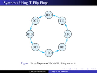
  • 15. Synthesis Using T Flip-Flops Figure: State diagram of three-bit binary counter D.R.V.L.B Thambawita DESIGN PROCEDURE
  • 16. Synthesis Using T Flip-Flops Figure: State Table for Three-Bit Counter D.R.V.L.B Thambawita DESIGN PROCEDURE
  • 17. Synthesis Using T Flip-Flops Figure: Maps for three-bit binary counter D.R.V.L.B Thambawita DESIGN PROCEDURE
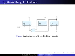
  • 18. Synthesis Using T Flip-Flops Figure: Logic diagram of three-bit binary counter D.R.V.L.B Thambawita DESIGN PROCEDURE