SlideShare a Scribd company logo
Let us assume, the below are the dimensions of the chip


                                                          Die


                                                          Core


                     www.vlsisystemdesign.com
Let’s explore how a city is planned


           www.vlsisystemdesign.com
Let’s explore how a city is planned


                                  Railway
 Hospital
                                  Station


                                  Water
Playground
                               Storage Tank


             www.vlsisystemdesign.com
Basic necessities and utilities are pre-planned and positioned,
in a manner to have the best reachability by each citizen


                                             Railway
            Hospital
                                             Station


                                             Water
           Playground
                                          Storage Tank


                        www.vlsisystemdesign.com
In a similar fashion, we start planning the chip area, by prioritizing the location
of critical cells.


                                                                      Die


                                                                      Core


                              www.vlsisystemdesign.com
Crtical cells can be IP’s (memories, ALU, etc.) or std cells (clock Buffer, clock inverter, etc )


                                                                             Die


                                                                             Core


                                    www.vlsisystemdesign.com
Let us understand, what are IP’s, std cells and their architecture?


                                                                 Die


                                                                Core


                         www.vlsisystemdesign.com
IP is a reusable unit of logic, cell, or chip layout design that is the intellectual
property designed by any individual.

 IP are also sometimes offered as generic gate-level netlist. i.e. standard cells,
  and complex cells.

 It consists of transistor level layout for logical cells and complex cells, which
  are implemented using layout tools.

 Lets have a look into internal of IP’s


                                     www.vlsisystemdesign.com
Consider one of the most commonly used IP i.e. CMOS Inverter


           Vdd                                        Vdd


  In      Inverter   Out                         In            Out


           Vss                                        Vss


                      www.vlsisystemdesign.com
CMOS Inverter consist of P-MOS Transistor


        Vdd

                                                 PMOS – P Diff

In                 Out


        Vss


                   www.vlsisystemdesign.com
CMOS Inverter consist of N-MOS Transistor


        Vdd

                                                 PMOS – P Diff

In                Out

                                                 NMOS – N Diff


        Vss


                   www.vlsisystemdesign.com
CMOS Inverter consist of Polysilicon Gate.


                        Vdd
                                                              Poly Gate
                                                                           PMOS – P Diff

              In                  Out

                                                                           NMOS – N Diff


                        Vss


Note : At the component level, polysilicon has been used as the conducting gate
material in MOSFET and CMOS processing technologies.
                                   www.vlsisystemdesign.com
CMOS Inverter IN/ OUT Lines


     Vdd
                                           Poly Gate
                                                       PMOS – P Diff

In             Out                  In

                                                       NMOS – N Diff


     Vss


                www.vlsisystemdesign.com
CMOS Inverter IN/ OUT Ports


     Vdd
                                           Poly Gate
                                                       PMOS – P Diff

In             Out                  In                      Out

                                                       NMOS – N Diff


     Vss


                www.vlsisystemdesign.com
CMOS Inverter Vdd & Vss Ports.


                                                       Vdd

     Vdd
                                           Poly Gate
                                                         PMOS – P Diff

In              Out                 In                        Out

                                                         NMOS – N Diff


     Vss
                                                       Vss


                www.vlsisystemdesign.com
Lets draw preliminary layout of inverter using stick diagram


                   www.vlsisystemdesign.com
Lets draw preliminary layout of inverter using stick diagram


Stick Diagrams are useful for planning the layout and routing of integrated circuits.

Every Line of a conducting material layer is represented by a line of a distinct color.


                                www.vlsisystemdesign.com
Lets draw preliminary layout of inverter using stick diagram


Stick Diagrams are useful for planning the layout and routing of integrated circuits.

Every Line of a conducting material layer is represented by a line of a distinct color.


                                                Polysilicon Gate


                                               P Diffusion


                                               N Diffusion

                                               Metal


                                                Contact

                                www.vlsisystemdesign.com
P-MOS Transistor represented by Bottle Green Color line


         PMOS – P Diff                                    P Diff


                     www.vlsisystemdesign.com
N-MOS Transistor represented by a Apple Green Color line


        PMOS – P Diff                                      P Diff


        NMOS – N Diff                                      N Diff


                    www.vlsisystemdesign.com
Polysilicon gates represented by Brown Color line


Poly Gate                                                       Poly
                   PMOS – P Diff                                       P Diff


                   NMOS – N Diff                                       N Diff


                                www.vlsisystemdesign.com
Metal is represented by Bottle Blue Color line


     Poly Gate                                                       Poly
                        PMOS – P Diff                                       P Diff

In                                                              In

                        NMOS – N Diff                                       N Diff


                                     www.vlsisystemdesign.com
Contacts are represented by Black Cross


     Poly Gate                                                      Poly
                        PMOS – P Diff                                           P Diff

In                                                             In

                        NMOS – N Diff                                           N Diff


                                                                    = Contact


                                    www.vlsisystemdesign.com
Metal is represented by Bottle Blue Color line


     Poly Gate                                                       Poly
                        PMOS – P Diff                                            P Diff

In                            Out                               In                  Out

                        NMOS – N Diff                                            N Diff


                                                                     = Contact


                                     www.vlsisystemdesign.com
Contacts are represented by Black Cross


     Poly Gate                                                      Poly
                        PMOS – P Diff                                           P Diff

In                           Out                               In                  Out

                        NMOS – N Diff                                           N Diff


                                                                    = Contact


                                    www.vlsisystemdesign.com
Metal is represented by Bottle Blue Color line


                     Vdd                                               Vdd


     Poly Gate                                                       Poly
                        PMOS – P Diff                                            P Diff

In                            Out                               In                  Out

                        NMOS – N Diff                                            N Diff


                     Vss                                               Vss


                                                                     = Contact


                                     www.vlsisystemdesign.com
Stick Diagrams are converted to Cell Layout by assigning length and width to the Wire


            Vdd                                                    Vdd


         Poly                                                    Poly
                        P Diff                                               P Diff

In                         Out                              In                  Out

                        N Diff                                               N Diff


           Vss                                                     Vss


         = Contact                                               = Contact


                                 www.vlsisystemdesign.com
Stick Diagrams are converted to Cell Layout by assigning length and width to the Wire


                                    Vdd
                                                         Width (w)

                                Poly
                                                     P Diff

                       In                                 Out

                                                     N Diff


                                    Vss


                                 = Contact


                              www.vlsisystemdesign.com
Stick Diagrams are converted to Cell Layout by assigning length and width to the Wire


                                    Vdd
                                                         Width (w)
                                 Length (L)
                                Poly
                                                     P Diff

                       In                                 Out

                                                     N Diff


                                    Vss


                                 = Contact


                              www.vlsisystemdesign.com
Cell Layout is a Black Box for IP User.

                                                              Vdd
       Vdd
                       Width (w)
     Length (L)
     Poly                                                   Poly
                     P Diff                                             P Diff

In                      Out                   In                                 Out

                     N Diff                                             N Diff


       Vss

                                                              Vss
     = Contact                                              = Contact


                                www.vlsisystemdesign.com
In Black Box, internal architecture counts less compared to IP Functionality

              Vdd                                                Vdd


          Poly                                                Poly
                          P Diff                                             P Diff

In                                    Out        In                                   Out

                          N Diff                                             N Diff


             Vss                                                Vss
           = Contact                                          = Contact


                                   www.vlsisystemdesign.com
IP’s serves the purpose of the Circuit design
                        i.e. Inverter in this case
       Vdd


                                                              Vdd
     Poly
                     P Diff

In                               Out                     In         Out

                     N Diff

                                                              Vss


       Vss
     = Contact


                              www.vlsisystemdesign.com
Similarly, other IP’s available as blocks :


                    www.vlsisystemdesign.com
Similarly, other IP’s available as blocks :


      Vdd


In1
      AND          Out
In2


      Vss


                                www.vlsisystemdesign.com
Similarly, other IP’s available as blocks :


      Vdd                               Vdd


In1                          In1
      AND          Out                  OR            Out
In2                          In2


      Vss                               Vss


                                www.vlsisystemdesign.com
Similarly, other IP’s available as blocks :


      Vdd                               Vdd                       Vdd


In1                          In1                            In1
      AND          Out                  OR            Out         NAND   Out
In2                          In2                            In2


      Vss                               Vss                       Vss


                                www.vlsisystemdesign.com
Complex blocks are also offered as IP’s


                  www.vlsisystemdesign.com
Complex blocks are also offered as IP’s


     Vdd


In              Out


     Vss


                       www.vlsisystemdesign.com
Complex blocks are also offered as IP’s

     Buffer is nothing but two inverters connected back-to-back

         Vdd


In                  Out


         Vss


                           www.vlsisystemdesign.com
Complex blocks are also offered as IP’s

     Buffer is nothing but two inverters connected back-to-back

         Vdd                                               Vdd    Vdd


In                  Out                               In                Out


         Vss                                               Vss    Vss


                           www.vlsisystemdesign.com
Complex blocks are also offered as IP’s

           Buffer is nothing but two inverters connected back-to-back

     Vdd        Vdd


In                          Out


     Vss        Vss


                                  www.vlsisystemdesign.com
Complex blocks are also offered as IP’s

           Buffer is nothing but two inverters connected back-to-back

     Vdd        Vdd                                          Vdd                 Vdd


                                                         Poly                   Poly
                                                                   P Diff              P Diff
In                          Out              In                        In Out                   Out
                                                                   N Diff              N Diff


     Vss        Vss


                                  www.vlsisystemdesign.com
Complex blocks are also offered as IP’s

           Buffer is nothing but two inverters connected back-to-back

     Vdd        Vdd                                               Vdd


In                          Out                              In   Buffer   Out


     Vss        Vss                                               Vss


                                  www.vlsisystemdesign.com
IP’s are offered in form of rectangular/square boxes


                  www.vlsisystemdesign.com
IP’s are offered in form of rectangular/square boxes
For E.g. The Buffer IP, will be represented as below


                   www.vlsisystemdesign.com
IP’s are offered in form of rectangular/square boxes
        For E.g. The Buffer IP, will be represented as below


     Vdd


In   Buffer     Out                                            Buffer


     Vss


                           www.vlsisystemdesign.com
IP’s are offered in form of rectangular/square boxes
For E.g. The AND Gate IP, will be represented as below


                  www.vlsisystemdesign.com
IP’s are offered in form of rectangular/square boxes
            For E.g. The AND Gate IP, will be represented as below


      Vdd


In1
      AND         Out                                                AND
In2


      Vss


                              www.vlsisystemdesign.com
Commonly asked Question
How do we differentiate between Vdd and Vss ?


                         www.vlsisystemdesign.com
Commonly asked Question
How do we differentiate between Vdd and Vss ?

It is represented in below pattern.
A Cross line on the bottom left of the Block represents Vss and top corner Vdd


                            www.vlsisystemdesign.com
Commonly asked Question
How do we differentiate between Vdd and Vss ?

It is represented in below pattern.
A Cross line on the bottom left of the Block represents Vss and top corner Vdd


                                                                       Vdd


    Buffer                                                   Buffer

                                                                       Vss

                                                                       Vdd

     AND                                                     AND


                                                                       Vss


                            www.vlsisystemdesign.com
Complex blocks e.g. ALU


             ALU
         www.vlsisystemdesign.com
Complex blocks e.g. ALU will be represented as below IP Block


                        ALU
                    www.vlsisystemdesign.com
• Memory is also a Complex IP used commonly.

• It is necessary to pre-define the geometrical location of these IP’s on a chip,
  so that the automated PNR tools do not modify their locations

• These cells are referred to as Pre-placed cells


                               www.vlsisystemdesign.com
Die


                           Core


www.vlsisystemdesign.com
Block a


                                     Die


                                     Core


          www.vlsisystemdesign.com
Block a       Block b


                                     Die


                                     Core


          www.vlsisystemdesign.com
Block a         Block b


      Block c


                                     Die


                                     Core


          www.vlsisystemdesign.com
Block a         Block b
Pre-placed
   Cells
                   Block c


                                                  Die


                                                  Core


                       www.vlsisystemdesign.com
Thus we have defined the Location of Pre-placed Cell in Chip


                    Block a         Block b
Pre-placed
   Cells
                          Block c


                                                                            Die


                                                                            Core

                              www.vlsisystemdesign.com

More Related Content

PPTX
Powerplanning
PDF
Basic synthesis flow and commands in digital VLSI
DOCX
Pd flow i
PDF
VLSI-Physical Design- Tool Terminalogy
PPTX
Floor plan & Power Plan
PPT
Placement and routing in full custom physical design
PDF
Implementing Useful Clock Skew Using Skew Groups
PPTX
ASIC Design Flow | Physical Design | VLSI
Powerplanning
Basic synthesis flow and commands in digital VLSI
Pd flow i
VLSI-Physical Design- Tool Terminalogy
Floor plan & Power Plan
Placement and routing in full custom physical design
Implementing Useful Clock Skew Using Skew Groups
ASIC Design Flow | Physical Design | VLSI

What's hot (20)

PDF
Clock Tree Synthesis.pdf
PDF
Floorplanning
PDF
Physical design-complete
PPTX
Placement in VLSI Design
PDF
3_DVD_IC_Fabrication_Flow_designer_perspective.pdf
ODP
Inputs of physical design
PPTX
VLSI Physical Design Flow(http://www.vlsisystemdesign.com)
DOCX
Power Reduction Techniques
PPTX
Vlsi Synthesis
PPTX
Vlsi physical design (Back End Process)
PPTX
Physical design
PPTX
PDF
Physical design
PPTX
Complete ASIC design flow - VLSI UNIVERSE
PPTX
Define Width and Height of Core and Die (http://www.vlsisystemdesign.com/PD-F...
PDF
Understanding cts log_messages
PPTX
ASIC DESIGN FLOW
PDF
Chapter1.slides
PPTX
Synopsys Fusion Compiler-Comprehensive RTL-to-GDSII Implementation System
PPTX
Physical Design Flow Challenges at 28nm on Multi-million Gate Blocks
Clock Tree Synthesis.pdf
Floorplanning
Physical design-complete
Placement in VLSI Design
3_DVD_IC_Fabrication_Flow_designer_perspective.pdf
Inputs of physical design
VLSI Physical Design Flow(http://www.vlsisystemdesign.com)
Power Reduction Techniques
Vlsi Synthesis
Vlsi physical design (Back End Process)
Physical design
Physical design
Complete ASIC design flow - VLSI UNIVERSE
Define Width and Height of Core and Die (http://www.vlsisystemdesign.com/PD-F...
Understanding cts log_messages
ASIC DESIGN FLOW
Chapter1.slides
Synopsys Fusion Compiler-Comprehensive RTL-to-GDSII Implementation System
Physical Design Flow Challenges at 28nm on Multi-million Gate Blocks
Ad

Viewers also liked (16)

PPTX
Floorplan (http://www.vlsisystemdesign.com/PD-Flow.php)
PPTX
Place decap
PPT
X$Tables And Sga Scanner, DOAG2009
PPTX
Java 8 Streams And Common Operations By Harmeet Singh(Taara)
PPTX
Buffer and scanner
PPTX
java: basics, user input, data type, constructor
PPT
1 java - data type
PDF
Jnp
PPTX
Understanding java streams
PDF
PPSX
Esoft Metro Campus - Certificate in java basics
PPT
Object-Oriented Analysis and Design
PPTX
Structured Vs, Object Oriented Analysis and Design
PDF
Vlsi interview questions1
PPTX
Switching activity
PPT
Object Oriented Analysis and Design
Floorplan (http://www.vlsisystemdesign.com/PD-Flow.php)
Place decap
X$Tables And Sga Scanner, DOAG2009
Java 8 Streams And Common Operations By Harmeet Singh(Taara)
Buffer and scanner
java: basics, user input, data type, constructor
1 java - data type
Jnp
Understanding java streams
Esoft Metro Campus - Certificate in java basics
Object-Oriented Analysis and Design
Structured Vs, Object Oriented Analysis and Design
Vlsi interview questions1
Switching activity
Object Oriented Analysis and Design
Ad

Similar to Define location of Preplaced cells(http://www.vlsisystemdesign.com/PD-Flow.php) (20)

DOC
Industrial training report of vlsi,vhdl and pcb designing
PPT
Lecture01
PDF
7 pg diploma ic layout design
PDF
L1 print
PPT
Vlsi giet
PPT
lecture 1 layout presentation of very large scale integration in digital elec...
PPT
chapter 1.ppt
PDF
Vlsi Summer training report pdf
PPTX
MetroScientific Week 1.pptx
PPT
Introduction to CMOS VLSI design Stick diagram.ppt
PDF
Lecture on Introduction to VLSI circuits and layouts
PPT
CMOS transistor and its concepts related
PPT
Ee213 vlsi introduction
PDF
Cmos uma
PDF
Cmos uma
PPT
CMOS VLSI Design.312313131312pp3213123213313123t
PPT
EC6601 VLSI Design CMOS Fabrication
PDF
VLSI DESIGN ITS ANALYSIS AND APPLICATIONS
PPT
Analog vlsi
PDF
Lecture 0.pdf
Industrial training report of vlsi,vhdl and pcb designing
Lecture01
7 pg diploma ic layout design
L1 print
Vlsi giet
lecture 1 layout presentation of very large scale integration in digital elec...
chapter 1.ppt
Vlsi Summer training report pdf
MetroScientific Week 1.pptx
Introduction to CMOS VLSI design Stick diagram.ppt
Lecture on Introduction to VLSI circuits and layouts
CMOS transistor and its concepts related
Ee213 vlsi introduction
Cmos uma
Cmos uma
CMOS VLSI Design.312313131312pp3213123213313123t
EC6601 VLSI Design CMOS Fabrication
VLSI DESIGN ITS ANALYSIS AND APPLICATIONS
Analog vlsi
Lecture 0.pdf

Recently uploaded (20)

PDF
Physiotherapy_for_Respiratory_and_Cardiac_Problems WEBBER.pdf
PPTX
PPH.pptx obstetrics and gynecology in nursing
PDF
VCE English Exam - Section C Student Revision Booklet
PDF
Basic Mud Logging Guide for educational purpose
PPTX
Institutional Correction lecture only . . .
PPTX
Pharmacology of Heart Failure /Pharmacotherapy of CHF
PPTX
Microbial diseases, their pathogenesis and prophylaxis
PPTX
Lesson notes of climatology university.
PDF
Saundersa Comprehensive Review for the NCLEX-RN Examination.pdf
PPTX
school management -TNTEU- B.Ed., Semester II Unit 1.pptx
PPTX
Cell Structure & Organelles in detailed.
PDF
The Lost Whites of Pakistan by Jahanzaib Mughal.pdf
PPTX
Pharma ospi slides which help in ospi learning
PDF
Classroom Observation Tools for Teachers
PDF
01-Introduction-to-Information-Management.pdf
PDF
BÀI TẬP BỔ TRỢ 4 KỸ NĂNG TIẾNG ANH 9 GLOBAL SUCCESS - CẢ NĂM - BÁM SÁT FORM Đ...
PPTX
IMMUNITY IMMUNITY refers to protection against infection, and the immune syst...
PDF
Sports Quiz easy sports quiz sports quiz
PDF
2.FourierTransform-ShortQuestionswithAnswers.pdf
PDF
RMMM.pdf make it easy to upload and study
Physiotherapy_for_Respiratory_and_Cardiac_Problems WEBBER.pdf
PPH.pptx obstetrics and gynecology in nursing
VCE English Exam - Section C Student Revision Booklet
Basic Mud Logging Guide for educational purpose
Institutional Correction lecture only . . .
Pharmacology of Heart Failure /Pharmacotherapy of CHF
Microbial diseases, their pathogenesis and prophylaxis
Lesson notes of climatology university.
Saundersa Comprehensive Review for the NCLEX-RN Examination.pdf
school management -TNTEU- B.Ed., Semester II Unit 1.pptx
Cell Structure & Organelles in detailed.
The Lost Whites of Pakistan by Jahanzaib Mughal.pdf
Pharma ospi slides which help in ospi learning
Classroom Observation Tools for Teachers
01-Introduction-to-Information-Management.pdf
BÀI TẬP BỔ TRỢ 4 KỸ NĂNG TIẾNG ANH 9 GLOBAL SUCCESS - CẢ NĂM - BÁM SÁT FORM Đ...
IMMUNITY IMMUNITY refers to protection against infection, and the immune syst...
Sports Quiz easy sports quiz sports quiz
2.FourierTransform-ShortQuestionswithAnswers.pdf
RMMM.pdf make it easy to upload and study

Define location of Preplaced cells(http://www.vlsisystemdesign.com/PD-Flow.php)

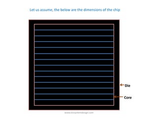
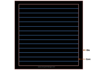
  • 1. Let us assume, the below are the dimensions of the chip Die Core www.vlsisystemdesign.com
  • 2. Let’s explore how a city is planned www.vlsisystemdesign.com
  • 3. Let’s explore how a city is planned Railway Hospital Station Water Playground Storage Tank www.vlsisystemdesign.com
  • 4. Basic necessities and utilities are pre-planned and positioned, in a manner to have the best reachability by each citizen Railway Hospital Station Water Playground Storage Tank www.vlsisystemdesign.com
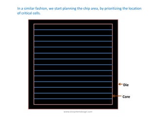
  • 5. In a similar fashion, we start planning the chip area, by prioritizing the location of critical cells. Die Core www.vlsisystemdesign.com
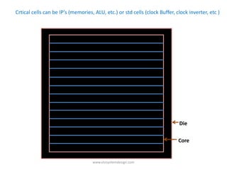
  • 6. Crtical cells can be IP’s (memories, ALU, etc.) or std cells (clock Buffer, clock inverter, etc ) Die Core www.vlsisystemdesign.com
  • 7. Let us understand, what are IP’s, std cells and their architecture? Die Core www.vlsisystemdesign.com
  • 8. IP is a reusable unit of logic, cell, or chip layout design that is the intellectual property designed by any individual.  IP are also sometimes offered as generic gate-level netlist. i.e. standard cells, and complex cells.  It consists of transistor level layout for logical cells and complex cells, which are implemented using layout tools.  Lets have a look into internal of IP’s www.vlsisystemdesign.com
  • 9. Consider one of the most commonly used IP i.e. CMOS Inverter Vdd Vdd In Inverter Out In Out Vss Vss www.vlsisystemdesign.com
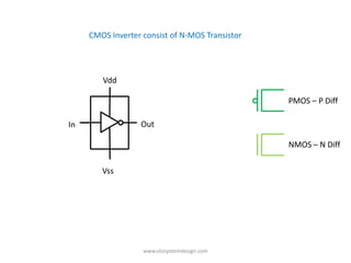
  • 10. CMOS Inverter consist of P-MOS Transistor Vdd PMOS – P Diff In Out Vss www.vlsisystemdesign.com
  • 11. CMOS Inverter consist of N-MOS Transistor Vdd PMOS – P Diff In Out NMOS – N Diff Vss www.vlsisystemdesign.com
  • 12. CMOS Inverter consist of Polysilicon Gate. Vdd Poly Gate PMOS – P Diff In Out NMOS – N Diff Vss Note : At the component level, polysilicon has been used as the conducting gate material in MOSFET and CMOS processing technologies. www.vlsisystemdesign.com
  • 13. CMOS Inverter IN/ OUT Lines Vdd Poly Gate PMOS – P Diff In Out In NMOS – N Diff Vss www.vlsisystemdesign.com
  • 14. CMOS Inverter IN/ OUT Ports Vdd Poly Gate PMOS – P Diff In Out In Out NMOS – N Diff Vss www.vlsisystemdesign.com
  • 15. CMOS Inverter Vdd & Vss Ports. Vdd Vdd Poly Gate PMOS – P Diff In Out In Out NMOS – N Diff Vss Vss www.vlsisystemdesign.com
  • 16. Lets draw preliminary layout of inverter using stick diagram www.vlsisystemdesign.com
  • 17. Lets draw preliminary layout of inverter using stick diagram Stick Diagrams are useful for planning the layout and routing of integrated circuits. Every Line of a conducting material layer is represented by a line of a distinct color. www.vlsisystemdesign.com
  • 18. Lets draw preliminary layout of inverter using stick diagram Stick Diagrams are useful for planning the layout and routing of integrated circuits. Every Line of a conducting material layer is represented by a line of a distinct color. Polysilicon Gate P Diffusion N Diffusion Metal Contact www.vlsisystemdesign.com
  • 19. P-MOS Transistor represented by Bottle Green Color line PMOS – P Diff P Diff www.vlsisystemdesign.com
  • 20. N-MOS Transistor represented by a Apple Green Color line PMOS – P Diff P Diff NMOS – N Diff N Diff www.vlsisystemdesign.com
  • 21. Polysilicon gates represented by Brown Color line Poly Gate Poly PMOS – P Diff P Diff NMOS – N Diff N Diff www.vlsisystemdesign.com
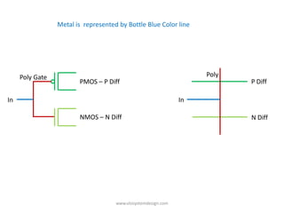
  • 22. Metal is represented by Bottle Blue Color line Poly Gate Poly PMOS – P Diff P Diff In In NMOS – N Diff N Diff www.vlsisystemdesign.com
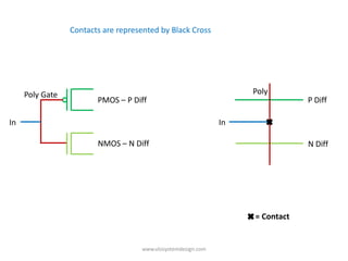
  • 23. Contacts are represented by Black Cross Poly Gate Poly PMOS – P Diff P Diff In In NMOS – N Diff N Diff = Contact www.vlsisystemdesign.com
  • 24. Metal is represented by Bottle Blue Color line Poly Gate Poly PMOS – P Diff P Diff In Out In Out NMOS – N Diff N Diff = Contact www.vlsisystemdesign.com
  • 25. Contacts are represented by Black Cross Poly Gate Poly PMOS – P Diff P Diff In Out In Out NMOS – N Diff N Diff = Contact www.vlsisystemdesign.com
  • 26. Metal is represented by Bottle Blue Color line Vdd Vdd Poly Gate Poly PMOS – P Diff P Diff In Out In Out NMOS – N Diff N Diff Vss Vss = Contact www.vlsisystemdesign.com
  • 27. Metal is represented by Bottle Blue Color line Vdd Vdd Poly Gate Poly PMOS – P Diff P Diff In Out In Out NMOS – N Diff N Diff Vss Vss = Contact www.vlsisystemdesign.com
  • 28. Stick Diagrams are converted to Cell Layout by assigning length and width to the Wire Vdd Vdd Poly Poly P Diff P Diff In Out In Out N Diff N Diff Vss Vss = Contact = Contact www.vlsisystemdesign.com
  • 29. Stick Diagrams are converted to Cell Layout by assigning length and width to the Wire Vdd Width (w) Poly P Diff In Out N Diff Vss = Contact www.vlsisystemdesign.com
  • 30. Stick Diagrams are converted to Cell Layout by assigning length and width to the Wire Vdd Width (w) Length (L) Poly P Diff In Out N Diff Vss = Contact www.vlsisystemdesign.com
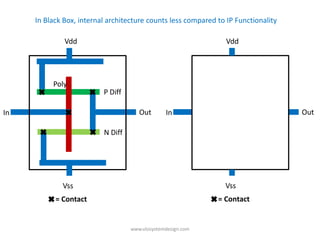
  • 31. Cell Layout is a Black Box for IP User. Vdd Vdd Width (w) Length (L) Poly Poly P Diff P Diff In Out In Out N Diff N Diff Vss Vss = Contact = Contact www.vlsisystemdesign.com
  • 32. In Black Box, internal architecture counts less compared to IP Functionality Vdd Vdd Poly Poly P Diff P Diff In Out In Out N Diff N Diff Vss Vss = Contact = Contact www.vlsisystemdesign.com
  • 33. IP’s serves the purpose of the Circuit design i.e. Inverter in this case Vdd Vdd Poly P Diff In Out In Out N Diff Vss Vss = Contact www.vlsisystemdesign.com
  • 34. Similarly, other IP’s available as blocks : www.vlsisystemdesign.com
  • 35. Similarly, other IP’s available as blocks : Vdd In1 AND Out In2 Vss www.vlsisystemdesign.com
  • 36. Similarly, other IP’s available as blocks : Vdd Vdd In1 In1 AND Out OR Out In2 In2 Vss Vss www.vlsisystemdesign.com
  • 37. Similarly, other IP’s available as blocks : Vdd Vdd Vdd In1 In1 In1 AND Out OR Out NAND Out In2 In2 In2 Vss Vss Vss www.vlsisystemdesign.com
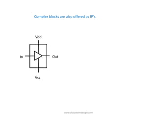
  • 38. Complex blocks are also offered as IP’s www.vlsisystemdesign.com
  • 39. Complex blocks are also offered as IP’s Vdd In Out Vss www.vlsisystemdesign.com
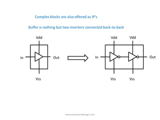
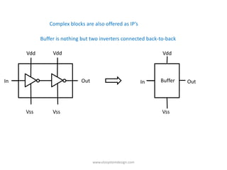
  • 40. Complex blocks are also offered as IP’s Buffer is nothing but two inverters connected back-to-back Vdd In Out Vss www.vlsisystemdesign.com
  • 41. Complex blocks are also offered as IP’s Buffer is nothing but two inverters connected back-to-back Vdd Vdd Vdd In Out In Out Vss Vss Vss www.vlsisystemdesign.com
  • 42. Complex blocks are also offered as IP’s Buffer is nothing but two inverters connected back-to-back Vdd Vdd In Out Vss Vss www.vlsisystemdesign.com
  • 43. Complex blocks are also offered as IP’s Buffer is nothing but two inverters connected back-to-back Vdd Vdd Vdd Vdd Poly Poly P Diff P Diff In Out In In Out Out N Diff N Diff Vss Vss www.vlsisystemdesign.com
  • 44. Complex blocks are also offered as IP’s Buffer is nothing but two inverters connected back-to-back Vdd Vdd Vdd In Out In Buffer Out Vss Vss Vss www.vlsisystemdesign.com
  • 45. IP’s are offered in form of rectangular/square boxes www.vlsisystemdesign.com
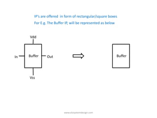
  • 46. IP’s are offered in form of rectangular/square boxes For E.g. The Buffer IP, will be represented as below www.vlsisystemdesign.com
  • 47. IP’s are offered in form of rectangular/square boxes For E.g. The Buffer IP, will be represented as below Vdd In Buffer Out Buffer Vss www.vlsisystemdesign.com
  • 48. IP’s are offered in form of rectangular/square boxes For E.g. The AND Gate IP, will be represented as below www.vlsisystemdesign.com
  • 49. IP’s are offered in form of rectangular/square boxes For E.g. The AND Gate IP, will be represented as below Vdd In1 AND Out AND In2 Vss www.vlsisystemdesign.com
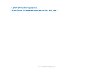
  • 50. Commonly asked Question How do we differentiate between Vdd and Vss ? www.vlsisystemdesign.com
  • 51. Commonly asked Question How do we differentiate between Vdd and Vss ? It is represented in below pattern. A Cross line on the bottom left of the Block represents Vss and top corner Vdd www.vlsisystemdesign.com
  • 52. Commonly asked Question How do we differentiate between Vdd and Vss ? It is represented in below pattern. A Cross line on the bottom left of the Block represents Vss and top corner Vdd Vdd Buffer Buffer Vss Vdd AND AND Vss www.vlsisystemdesign.com
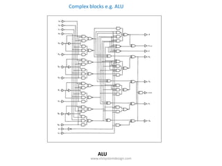
  • 53. Complex blocks e.g. ALU ALU www.vlsisystemdesign.com
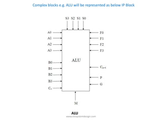
  • 54. Complex blocks e.g. ALU will be represented as below IP Block ALU www.vlsisystemdesign.com
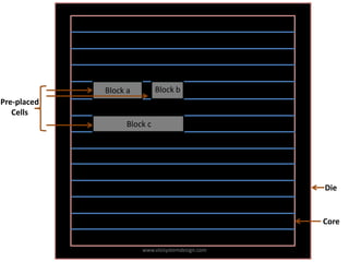
  • 55. • Memory is also a Complex IP used commonly. • It is necessary to pre-define the geometrical location of these IP’s on a chip, so that the automated PNR tools do not modify their locations • These cells are referred to as Pre-placed cells www.vlsisystemdesign.com
  • 56. Die Core www.vlsisystemdesign.com
  • 57. Block a Die Core www.vlsisystemdesign.com
  • 58. Block a Block b Die Core www.vlsisystemdesign.com
  • 59. Block a Block b Block c Die Core www.vlsisystemdesign.com
  • 60. Block a Block b Pre-placed Cells Block c Die Core www.vlsisystemdesign.com
  • 61. Thus we have defined the Location of Pre-placed Cell in Chip Block a Block b Pre-placed Cells Block c Die Core www.vlsisystemdesign.com